EP1511263A2 - Methode und Vorrichtung für mehrstufige Quadratur-Amplitudenmodulation - Google Patents
Methode und Vorrichtung für mehrstufige Quadratur-Amplitudenmodulation Download PDFInfo
- Publication number
- EP1511263A2 EP1511263A2 EP04025350A EP04025350A EP1511263A2 EP 1511263 A2 EP1511263 A2 EP 1511263A2 EP 04025350 A EP04025350 A EP 04025350A EP 04025350 A EP04025350 A EP 04025350A EP 1511263 A2 EP1511263 A2 EP 1511263A2
- Authority
- EP
- European Patent Office
- Prior art keywords
- level
- quadrature amplitude
- signal
- digital
- digital filter
- Prior art date
- Legal status (The legal status is an assumption and is not a legal conclusion. Google has not performed a legal analysis and makes no representation as to the accuracy of the status listed.)
- Granted
Links
Images


Classifications
-
- H—ELECTRICITY
- H04—ELECTRIC COMMUNICATION TECHNIQUE
- H04L—TRANSMISSION OF DIGITAL INFORMATION, e.g. TELEGRAPHIC COMMUNICATION
- H04L27/00—Modulated-carrier systems
- H04L27/32—Carrier systems characterised by combinations of two or more of the types covered by groups H04L27/02, H04L27/10, H04L27/18 or H04L27/26
- H04L27/34—Amplitude- and phase-modulated carrier systems, e.g. quadrature-amplitude modulated carrier systems
- H04L27/36—Modulator circuits; Transmitter circuits
- H04L27/362—Modulation using more than one carrier, e.g. with quadrature carriers, separately amplitude modulated
-
- H—ELECTRICITY
- H04—ELECTRIC COMMUNICATION TECHNIQUE
- H04L—TRANSMISSION OF DIGITAL INFORMATION, e.g. TELEGRAPHIC COMMUNICATION
- H04L1/00—Arrangements for detecting or preventing errors in the information received
- H04L1/0001—Systems modifying transmission characteristics according to link quality, e.g. power backoff
- H04L1/0002—Systems modifying transmission characteristics according to link quality, e.g. power backoff by adapting the transmission rate
- H04L1/0003—Systems modifying transmission characteristics according to link quality, e.g. power backoff by adapting the transmission rate by switching between different modulation schemes
-
- H—ELECTRICITY
- H04—ELECTRIC COMMUNICATION TECHNIQUE
- H04L—TRANSMISSION OF DIGITAL INFORMATION, e.g. TELEGRAPHIC COMMUNICATION
- H04L27/00—Modulated-carrier systems
- H04L27/32—Carrier systems characterised by combinations of two or more of the types covered by groups H04L27/02, H04L27/10, H04L27/18 or H04L27/26
- H04L27/34—Amplitude- and phase-modulated carrier systems, e.g. quadrature-amplitude modulated carrier systems
Definitions
- the present invention relates to a method and an apparatus for multi-level quadrature amplitude modulation used in a digital microwave communication system and more particularly to a method and an apparatus for multi-level quadrature amplitude modulation always setting a DC level to 0 irrespective of a modulation multi-level number.
- a multi-level quadrature amplitude modulation system such as 64 quadrature amplitude modulation (64 QAM) is used for aiming at effective utilization of a frequency band.
- a digital filter (a rolloff filter) for waveform shaping is required for a modulator and a demodulator, respectively.
- a digital filter for performing filtering by digital signal processing on the time base of the baseband has become to be put to practical use in recent years owing to progress of digital signal processing technique and working speed and integration degree of a device. Further, those digital filters that have no problems of dispersion and change with the passage of time of characteristics, temperature variation and so on have become to be realized.
- IIR Infinite Impulse Response
- FIR Finite Impulse Response
- Fig. 1 shows a block diagram of one channel portion of a rolloff filter on transmission side for QPSK composed of a conventional FIR type digital filter.
- a row of data are inputted from a terminal 81 and passes in a shift register 151.
- the data of respective registers are inputted to taps (multipliers) 411 to 416, and multiplied by tap coefficients.
- the outputs of respective taps 411 to 416 are inputted to an adder 311, and the outputs from all the taps are added and outputted.
- sampling values of impulse response corresponding to frequency characteristics of the digital filter become tap coefficients Cj (j is an integer from - N to N in the case of (2N+1) taps) of respective taps.
- the output bk of the digital filter is expressed as follows: and frequency characteristics corresponding to discrete Fourier transform of the tap coefficients Cj are given.
- the number of rows of the input signal at time of a modulation system of more multi-values is m/2 one channel when it is assumed that a modulation multi-level number is 2 m .
- a digital filter whose input bit number is i can also be used for a modulation system whose input bit number is i or below by using high order bits of the input.
- the output of the digital filter is inputted to a quadrature modulator after being converted into an analog signal by means of a D/A converter, but the quadrature modulator is direct-current-coupled with the D/A converter, and is adjusted at the original DC level. Thus, it becomes necessary to readjust the quadrature modulator when the DC level of the digital filter output is changed.
- the mean power is changed along with the increase of the multi-level number.
- the analog portion of the quadrature modulator has such a problem that, since power value levels (level diagram) of respective parts are set so that both the distortion characteristics and the S/N ratio satisfy request values, original characteristics can no longer be maintained when the input level of the quadrature modulator changes largely by setting of the multi-level number.
- a method that a level compensation circuit is provided between the output of a digital filter and a D/A converter, and the mean power of the input signals of the D/A converter becomes constant in the level compensation circuit irrespective of the modulation system has been proposed.
- the present method is set forth in Japanese Patent Laid-Open No. Hei 4-208741. This example is shown in Fig. 3.
- digital signal circuits 501 and 502 for signal row number portions perform cosine rolloff waveform processing of binary digital signals, respectively.
- a digital filter is composed of digital signal circuits 501 and 502 and adding circuits 511 and 512 for adding the outputs thereof.
- This is a structure referred to as a binary transversal filter (BTF) , but it is the same as the FIR type in point of the relationship of input vs. output.
- the outputs of the digital filter are inputted to D/A converters 531 and 532 through level compensation circuits 521 and 522 and converted into analog signals. Then, the signals are inputted into a quadrature modulator 540, and outputted as a modulated signal.
- the level compensation circuit is placed between the digital filters and the D/A converters (521, 522) or after 'the quadrature modulator at 550.
- the level compensation circuits 521 and 522 multiply the digital filter output by a constant by means of multipliers so that the output mean power becomes constant. Further, when the DC level is shifted, the level compensation circuits operate so that the DC level becomes constant by means of the adders.
- the level compensation circuit 550 is placed at the output of the quadrature modulator, the above-mentioned level compensation is performed by an analog multiplier.
- This level compensation circuit is composed of a read only memory (ROM) or a digital multiplier and an adder, the output of the digital filter is normally about 8 bits to 12 bits, and a circuit scale of a multiplier of the bit number in this order becomes considerably large. Furthermore, since over-sampling in the order of two times to eight times is made on the digital filter output based on a sampling theorem, the signal speed becomes considerably high. Therefore, a high speed performance is also required for the multiplier and the adder.
- the level compensation circuit is composed of a ROM, that which has a large number of bits of the address and is of a high speed is also required.
- the method of multi-level quadrature amplitude modulation of the present invention modulating at different modulation multi-level numbers, and comprises the steps of converting all of the input bit numbers into the same bit number based on a prescribed conversion rule for each orthogonal channel irrespective of the modulation multi-level number of the multi-level quadrature amplitude modulation system described above, filtering the converted signal by means of a digital filter, converting the output of the digital filter into an analog signal by means of a D/A converter, and modulating the analog signal by means of a quadrature modulator.
- the multi-level quadrature amplitude modulation system of the present invention is capable of modulation at different modulation multi-level numbers, and comprises a code converter for converting all of the input bit numbers into the same bit number based on a prescribed conversion rule for each orthogonal channel irrespective of the modulation multi-level number of the multi-level quadrature amplitude modulation system, a digital filter for applying waveform shaping to the output of the code converter, a D/A converter for converting the output of the digital filter into an analog signal, and a quadrature modulator for applying quadrature modulation to the output of the D/A converter.
- the prescribed conversion rule described above stipulates that, when the system is made to operate as a quadrature amplitude modulation system of a 2 m or 2 m-2n value (m is an integer of 4 or more, and n is an integer of 0 or more), a pattern "1,0,0," of a bit number (n+1) is added to lower order of the least significant bit of an input signal for the digital input signal in (m/2-n) row thus converting it into a signal in a (m/2+1) row, and the most significant bit of the signal in the (m/2+1) row is inverted thereby to convert it into a 2'complement.
- Fig. 4 shows a block diagram in the case of 64 QAM as an example of an apparatus for multi-level quadrature amplitude modulation.
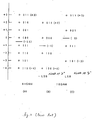
- Fig. 5 is a configuration table showing an embodiment of code conversion.
- code converters 10 and 20 Three rows in each orthogonal channel of input data signals in 6 rows of 64 QAM are inputted to code converters 10 and 20 for realizing a code conversion system of the present invention.
- code converters 10 and 20 code conversion shown in Fig. 5 is performed, and the outputs thereof are inputted to digital filters 11 and 21.
- the digital signals band-limited in the digital filters 11 and 21 are converted into analog signals by means of D/A converters 12 and 22, two orthogonal channels' portion is inputted thereafter in a quadrature modulator 30 and outputted as a modulated wave.
- the code converter has functions of bit addition to inputted bits and MSB inversion based on a fixed conversion rule. These functions can be gained in a comparatively simple manner using a digital signal processor (DSP) for instance.
- DSP digital signal processor
- the operation of the digital filters 11 and 21 is the same as explained as a related art, and these filters are FIR type digital filters.
- the quadrature modulator 30 multiplies the output signals of two D/A converters 12 and 22 by a carrier wave having phase difference of 90° , respectively, and adds the results thereof so as to output a quadrature modulated wave.
- the code conversion table shown in Fig. 5 will be explained.
- the number of input signal rows of one channel of the baseband of the modulator of 64 quadrature amplitude modulation (64 QAM) is three.
- the number of rows of input signals when a modulator of 64 QAM is used in a modulation system of a lower level such as 16 QAM may be two. In the present invention, however, this signal expressed in three bits or less is converted into 4 bits in accordance with a conversion rule described below for all of applicable modulation systems.
- the input signal in Fig. 5 is expressed by an offset binary code, and the output is expressed by a complement of 2.
- m/2 bits are required in 2 m QAM.
- the total bit number of an input signal is converted into the bit number (m/2) of one channel of the modulation system of the maximum multi-level number +1 bit.
- the 64 QAM which is a QAM modulation system in which the signal point number is power of an even number of 2 has been explained above.
- a QAM modulation system in which the signal point number such as 32 QAM is power of an odd number of 2 a part of signal points of a QAM system of power of an even number of 2 having the power number one above is used. Therefore, when it is made not to input a combination-forbidden signal, it is possible to apply the conversion system of the present invention as it is.
- the present invention is also applicable to a modulation system of higher multi-level such as 256 QAM.
- the apparatus for multi-level quadrature amplitude modulation of the present invention has such effects as follows.
Landscapes
- Engineering & Computer Science (AREA)
- Computer Networks & Wireless Communication (AREA)
- Signal Processing (AREA)
- Quality & Reliability (AREA)
- Digital Transmission Methods That Use Modulated Carrier Waves (AREA)
Priority Applications (1)
| Application Number | Priority Date | Filing Date | Title |
|---|---|---|---|
| DE69637220T DE69637220T3 (de) | 1995-07-12 | 1996-07-11 | Verfahren und Vorrichtung für mehrstufige Quadratur-Amplitudenmodulation |
Applications Claiming Priority (3)
| Application Number | Priority Date | Filing Date | Title |
|---|---|---|---|
| JP17598195 | 1995-07-12 | ||
| JP17598195 | 1995-07-12 | ||
| EP96111193A EP0753953B1 (de) | 1995-07-12 | 1996-07-11 | Methode und Vorrichtung für mehrstufige Quadratur-Amplitudenmodulation |
Related Parent Applications (2)
| Application Number | Title | Priority Date | Filing Date |
|---|---|---|---|
| EP96111193A Division EP0753953B1 (de) | 1995-07-12 | 1996-07-11 | Methode und Vorrichtung für mehrstufige Quadratur-Amplitudenmodulation |
| EP96111193.7 Division | 1996-07-11 |
Publications (4)
| Publication Number | Publication Date |
|---|---|
| EP1511263A2 true EP1511263A2 (de) | 2005-03-02 |
| EP1511263A3 EP1511263A3 (de) | 2005-11-23 |
| EP1511263B1 EP1511263B1 (de) | 2007-08-22 |
| EP1511263B2 EP1511263B2 (de) | 2011-08-24 |
Family
ID=16005622
Family Applications (4)
| Application Number | Title | Priority Date | Filing Date |
|---|---|---|---|
| EP04025350A Expired - Lifetime EP1511263B2 (de) | 1995-07-12 | 1996-07-11 | Verfahren und Vorrichtung für mehrstufige Quadratur-Amplitudenmodulation |
| EP07112246A Withdrawn EP1848171A1 (de) | 1995-07-12 | 1996-07-11 | Methode und Vorrichtung für mehrstufige Quadratur-Amplitudenmodulation |
| EP96111193A Expired - Lifetime EP0753953B1 (de) | 1995-07-12 | 1996-07-11 | Methode und Vorrichtung für mehrstufige Quadratur-Amplitudenmodulation |
| EP06013173A Withdrawn EP1699201A1 (de) | 1995-07-12 | 1996-07-11 | Methode und Vorrichtung für mehrstufige Quadratur-Amplitudenmodulation |
Family Applications After (3)
| Application Number | Title | Priority Date | Filing Date |
|---|---|---|---|
| EP07112246A Withdrawn EP1848171A1 (de) | 1995-07-12 | 1996-07-11 | Methode und Vorrichtung für mehrstufige Quadratur-Amplitudenmodulation |
| EP96111193A Expired - Lifetime EP0753953B1 (de) | 1995-07-12 | 1996-07-11 | Methode und Vorrichtung für mehrstufige Quadratur-Amplitudenmodulation |
| EP06013173A Withdrawn EP1699201A1 (de) | 1995-07-12 | 1996-07-11 | Methode und Vorrichtung für mehrstufige Quadratur-Amplitudenmodulation |
Country Status (4)
| Country | Link |
|---|---|
| US (1) | US5825828A (de) |
| EP (4) | EP1511263B2 (de) |
| JP (1) | JP3119167B2 (de) |
| DE (2) | DE69637220T3 (de) |
Families Citing this family (4)
| Publication number | Priority date | Publication date | Assignee | Title |
|---|---|---|---|---|
| DE19620843B4 (de) * | 1996-05-23 | 2005-08-11 | Siemens Ag | Verfahren zur Modulation eines Modulationsträgers und Mobil-Kommunikationssystem |
| US5945885A (en) * | 1998-03-05 | 1999-08-31 | Hewlett-Packard Company | Digital baseband modulator adaptable to different modulation types |
| CN103238304B (zh) * | 2011-10-26 | 2016-11-16 | 松下知识产权经营株式会社 | 多值振幅调制装置、多值振幅解调装置及使用它们的传送系统、以及多值振幅调制方法及多值振幅解调方法 |
| EP3038053B1 (de) | 2014-12-22 | 2019-11-06 | Reactive Reality GmbH | Verfahren und System zur Erzeugung von Kleidungsstückmusterdaten |
Family Cites Families (10)
| Publication number | Priority date | Publication date | Assignee | Title |
|---|---|---|---|---|
| US4520490A (en) * | 1983-08-05 | 1985-05-28 | At&T Information Systems Inc. | Differentially nonlinear convolutional channel coding with expanded set of signalling alphabets |
| CA1232022A (en) * | 1983-11-30 | 1988-01-26 | Eisuke Fukuda | Radio communication system |
| JPS60178753A (ja) * | 1984-02-24 | 1985-09-12 | Fujitsu Ltd | 直流オフセツト付加方式 |
| US4812786A (en) * | 1987-09-28 | 1989-03-14 | California Institute Of Technology | Method and system for providing precise multi-function modulation |
| JPH07114345B2 (ja) | 1988-05-28 | 1995-12-06 | 日本電気株式会社 | 変調装置 |
| IT1240444B (it) * | 1990-05-18 | 1993-12-16 | Borsano Corrado | Procedimento per l'attuazione della modulazione digitale multilivello mediante un elaboratore di segnali numerici |
| JPH04208741A (ja) * | 1990-11-30 | 1992-07-30 | Tech Res & Dev Inst Of Japan Def Agency | 多値直交振幅変調回路 |
| DE69222452T2 (de) * | 1991-03-11 | 1998-02-26 | Nippon Telegraph & Telephone | Quadraturamplitudenmodulator mit Verzerrungskompensation |
| JP3342877B2 (ja) * | 1991-05-27 | 2002-11-11 | 株式会社東芝 | ディジタル無線通信装置とその変調回路 |
| US5508748A (en) * | 1993-02-08 | 1996-04-16 | Zenith Electronics Corporation | Data level selection for multilevel VSB transmission system |
-
1996
- 1996-07-11 DE DE69637220T patent/DE69637220T3/de not_active Expired - Lifetime
- 1996-07-11 EP EP04025350A patent/EP1511263B2/de not_active Expired - Lifetime
- 1996-07-11 EP EP07112246A patent/EP1848171A1/de not_active Withdrawn
- 1996-07-11 US US08/678,100 patent/US5825828A/en not_active Expired - Lifetime
- 1996-07-11 EP EP96111193A patent/EP0753953B1/de not_active Expired - Lifetime
- 1996-07-11 DE DE69636298T patent/DE69636298T2/de not_active Expired - Lifetime
- 1996-07-11 JP JP08181718A patent/JP3119167B2/ja not_active Expired - Lifetime
- 1996-07-11 EP EP06013173A patent/EP1699201A1/de not_active Withdrawn
Also Published As
| Publication number | Publication date |
|---|---|
| EP0753953B1 (de) | 2006-06-28 |
| JP3119167B2 (ja) | 2000-12-18 |
| EP1848171A1 (de) | 2007-10-24 |
| DE69637220T3 (de) | 2012-02-02 |
| US5825828A (en) | 1998-10-20 |
| DE69636298D1 (de) | 2006-08-10 |
| EP1511263B2 (de) | 2011-08-24 |
| DE69637220D1 (de) | 2007-10-04 |
| EP0753953A1 (de) | 1997-01-15 |
| DE69636298T2 (de) | 2007-05-31 |
| EP1511263A3 (de) | 2005-11-23 |
| EP1511263B1 (de) | 2007-08-22 |
| JPH0983601A (ja) | 1997-03-28 |
| DE69637220T2 (de) | 2007-12-27 |
| EP1699201A1 (de) | 2006-09-06 |
Similar Documents
| Publication | Publication Date | Title |
|---|---|---|
| EP0776110B1 (de) | Quadraturmodulationsschaltung | |
| KR100646456B1 (ko) | 포스트 필터링 반송파 재결합을 이용하는 디지털 qam 변조기 | |
| US6404821B1 (en) | Digital beamformer for receiving a first number of information signals using a second number of antenna array elements | |
| US5459749A (en) | Multi-level superposed amplitude-modulated baseband signal processor | |
| EP0583059B1 (de) | System mit adaptiver Signalmodulation | |
| US4993047A (en) | Volterra linearizer for digital transmission | |
| JPH1023096A (ja) | ディジタル変調器および復調器 | |
| US4965536A (en) | Quadrature amplitude modulation system using digital filters | |
| US5825828A (en) | Method and apparatus for multi-level quadrature amplitude modulation | |
| US5657353A (en) | Pulse shaping filter for received digital transmissions using phase lock loop for adjusting shift register | |
| CA2037090C (en) | Modem comprising saw filters having opposite passband delay characteristics | |
| US6647076B1 (en) | Method of compensating for interference in a signal generated by discrete multitone modulation, and circuit configuration for carrying out the method. | |
| KR0182934B1 (ko) | 멀티스테이트 직교반송파 진폭변조 슬로프 등화기 | |
| JP3331978B2 (ja) | ディジタル無線通信装置の変調回路とその変調方法 | |
| JP3774350B2 (ja) | 多値デジタル変調信号復調回路 | |
| JP2705363B2 (ja) | 自動干渉除去装置 | |
| JP2000138648A (ja) | 逆フーリエ変換回路及び逆フーリエ変換方法 | |
| JPH04280144A (ja) | 帯域制限用ロールオフフィルタを用いたpsk変調用波形生成回路 | |
| JPH0738382A (ja) | ディジタルフィルタ | |
| JP2000278239A (ja) | 差動符号化離散フーリエ逆変換ハイブリッド回路 |
Legal Events
| Date | Code | Title | Description |
|---|---|---|---|
| PUAI | Public reference made under article 153(3) epc to a published international application that has entered the european phase |
Free format text: ORIGINAL CODE: 0009012 |
|
| AC | Divisional application: reference to earlier application |
Ref document number: 0753953 Country of ref document: EP Kind code of ref document: P |
|
| AK | Designated contracting states |
Kind code of ref document: A2 Designated state(s): DE FR IT |
|
| PUAL | Search report despatched |
Free format text: ORIGINAL CODE: 0009013 |
|
| AK | Designated contracting states |
Kind code of ref document: A3 Designated state(s): DE FR IT |
|
| RIC1 | Information provided on ipc code assigned before grant |
Ipc: 7H 04L 27/34 A Ipc: 7H 04L 25/49 B |
|
| 17P | Request for examination filed |
Effective date: 20051018 |
|
| AKX | Designation fees paid |
Designated state(s): DE FR IT |
|
| 17Q | First examination report despatched |
Effective date: 20060608 |
|
| 17Q | First examination report despatched |
Effective date: 20060608 |
|
| GRAP | Despatch of communication of intention to grant a patent |
Free format text: ORIGINAL CODE: EPIDOSNIGR1 |
|
| GRAS | Grant fee paid |
Free format text: ORIGINAL CODE: EPIDOSNIGR3 |
|
| GRAA | (expected) grant |
Free format text: ORIGINAL CODE: 0009210 |
|
| AC | Divisional application: reference to earlier application |
Ref document number: 0753953 Country of ref document: EP Kind code of ref document: P |
|
| AK | Designated contracting states |
Kind code of ref document: B1 Designated state(s): DE FR IT |
|
| REF | Corresponds to: |
Ref document number: 69637220 Country of ref document: DE Date of ref document: 20071004 Kind code of ref document: P |
|
| ET | Fr: translation filed | ||
| PLBI | Opposition filed |
Free format text: ORIGINAL CODE: 0009260 |
|
| PLBI | Opposition filed |
Free format text: ORIGINAL CODE: 0009260 |
|
| 26 | Opposition filed |
Opponent name: NERA NETWORKS A/S Effective date: 20080516 |
|
| PLAX | Notice of opposition and request to file observation + time limit sent |
Free format text: ORIGINAL CODE: EPIDOSNOBS2 |
|
| 26 | Opposition filed |
Opponent name: NERA NETWORKS A/S Effective date: 20080516 Opponent name: SIAE MICROELETTRONICA S.P.A. Effective date: 20080516 |
|
| PLBB | Reply of patent proprietor to notice(s) of opposition received |
Free format text: ORIGINAL CODE: EPIDOSNOBS3 |
|
| PLAY | Examination report in opposition despatched + time limit |
Free format text: ORIGINAL CODE: EPIDOSNORE2 |
|
| PLAH | Information related to despatch of examination report in opposition + time limit modified |
Free format text: ORIGINAL CODE: EPIDOSCORE2 |
|
| PLBC | Reply to examination report in opposition received |
Free format text: ORIGINAL CODE: EPIDOSNORE3 |
|
| PLBP | Opposition withdrawn |
Free format text: ORIGINAL CODE: 0009264 |
|
| PUAH | Patent maintained in amended form |
Free format text: ORIGINAL CODE: 0009272 |
|
| STAA | Information on the status of an ep patent application or granted ep patent |
Free format text: STATUS: PATENT MAINTAINED AS AMENDED |
|
| 27A | Patent maintained in amended form |
Effective date: 20110824 |
|
| AK | Designated contracting states |
Kind code of ref document: B2 Designated state(s): DE FR IT |
|
| REG | Reference to a national code |
Ref country code: DE Ref legal event code: R102 Ref document number: 69637220 Country of ref document: DE |
|
| REG | Reference to a national code |
Ref country code: DE Ref legal event code: R102 Ref document number: 69637220 Country of ref document: DE Effective date: 20110824 |
|
| REG | Reference to a national code |
Ref country code: FR Ref legal event code: PLFP Year of fee payment: 20 |
|
| PGFP | Annual fee paid to national office [announced via postgrant information from national office to epo] |
Ref country code: DE Payment date: 20150707 Year of fee payment: 20 |
|
| PGFP | Annual fee paid to national office [announced via postgrant information from national office to epo] |
Ref country code: FR Payment date: 20150629 Year of fee payment: 20 |
|
| PGFP | Annual fee paid to national office [announced via postgrant information from national office to epo] |
Ref country code: IT Payment date: 20150727 Year of fee payment: 20 |
|
| REG | Reference to a national code |
Ref country code: DE Ref legal event code: R071 Ref document number: 69637220 Country of ref document: DE |