EP1512078B1 - Programmierbare zugriffslatenzzeit in einem pseudo-multiportspeicher - Google Patents
Programmierbare zugriffslatenzzeit in einem pseudo-multiportspeicher Download PDFInfo
- Publication number
- EP1512078B1 EP1512078B1 EP03725527A EP03725527A EP1512078B1 EP 1512078 B1 EP1512078 B1 EP 1512078B1 EP 03725527 A EP03725527 A EP 03725527A EP 03725527 A EP03725527 A EP 03725527A EP 1512078 B1 EP1512078 B1 EP 1512078B1
- Authority
- EP
- European Patent Office
- Prior art keywords
- request
- facility
- queue
- memory
- signal
- Prior art date
- Legal status (The legal status is an assumption and is not a legal conclusion. Google has not performed a legal analysis and makes no representation as to the accuracy of the status listed.)
- Expired - Lifetime
Links
Images


Classifications
-
- G—PHYSICS
- G06—COMPUTING OR CALCULATING; COUNTING
- G06F—ELECTRIC DIGITAL DATA PROCESSING
- G06F13/00—Interconnection of, or transfer of information or other signals between, memories, input/output devices or central processing units
- G06F13/14—Handling requests for interconnection or transfer
- G06F13/16—Handling requests for interconnection or transfer for access to memory bus
- G06F13/1605—Handling requests for interconnection or transfer for access to memory bus based on arbitration
- G06F13/161—Handling requests for interconnection or transfer for access to memory bus based on arbitration with latency improvement
Definitions
- the invention relates to a computer memory arrangement, comprising a first plurality of input ports that are collectively coupled through a first router facility to selectively feed a second plurality of memory modules as has furthermore been recited in the preamble of Claim 1.
- Present-day computing facilities such as Digital Signal Processors (DSP) require both a great processing power, and also much communication traffic between memory and processor(s).
- DSP Digital Signal Processors
- both of these two performance aspects associated to the number of memory modules and processors, respectively, should be scalable, and in particular, the number of parallel data moves should be allowed to exceed the value of 2.
- US5559970 discloses a self-routing crossbar switch that interconnects a plurality of processors with a plurality of memory modules.
- a processor is connected to each input port and a memory module is connected to each output port.
- the crossbar switch of US5559970 comprises decoders respectively coupled to said input ports for distributing memory access requests from said processors to output ports among said N output ports which are designated as destination ports by said memory access requests.
- N first-in first-out buffers provided at respective outputs of said decoders and separated into N groups, each of said N groups containing N buffers connected to a common destination port; N N-input and N-output aligners, coupled to outputs of said respective groups of NxN first-in first-out buffers, for aligning effective memory access requests in series and N serializers connected to outputs of said respective aligners, for serializing the memory access requests aligned by said aligners and outputting to one of said output ports, wherein each of said N-input and N-output aligners includes, two (N/2)-input and (N/2)-output aligners, having two N/2 inputs, each of which correspond to a respective input of said N-input and N-output aligner, for aligning effective memory access requests in series; and an N-input and N-output router, having N inputs, each of which correspond to a respective output of said two (N/2)-input and (N/2)-output aligners, for shifting forward
- the invention also relates to a computer arrangement comprising a fourth plurality of load/store units interfaced to a computer memory arrangement as claimed in Claim 1. Further advantageous aspects of the invention are recited in dependent Claims.
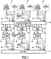
- Figure 1 illustrates a pseudo multiport data memory template or parametrizable embodiment.
- the template consists of an exemplary number of L building blocks (only the numbers 0, l, L-1 having been shown) that surround an array of B memory banks 20-24 (only the numbers 0, b, and B-1 having been shown), each provided with an intermediate queue 26-30 that has been put in parallel between the input and the output of the memory module in question.
- the memory banks represent a unified address map.
- the values relate according to B ⁇ L , but this is no restriction and in principle, the value of B may be as low as 1.
- the external access signals may as shown at the top of the Figure, emanate from respecive load/store unit facilites 17-19.
- Each access signal comprises a chip select cs, a w rite e na b le web, and each will furthermore present an address and write data. These signals will be sent to request/acknowledge router 32.
- each external access facility will also be able to receive external read data, as shown by the arrows such as arrow 35 from result router 34.
- the purposes of the blocks surrounding the memory banks are threefold. First, the access requests to the various memory banks are routed by router facility 32 from the appropriate write port to the correct memory bank, and furthermore, the access results from the various memory banks are routed back by router facility 34 from the appropriate memory bank towards the correct read port.
- each memory bank 20-24 has a dedicated bank arbiter 36-40 located in front thereof.
- the number of bank conflicts is reduced by extending the latency of the bank accesses by an additional slack interval above the unavoidable access latency that is associated to the memory banks proper.
- the additional slack is obtained through delaying the accesses in L parallel request queues 42-46, wherein L is the number of read/write ports, and furthermore through delaying the results in B parallel result queues 48-52, wherein B is the number of memory banks.
- the request queues 42-46 may delay input requests over a time as depending on the circumstances.
- a supplemental delay in the result queues 48-52 may produce an overall delay between the actual request and the instant that the result becomes available at the output port, wherein the overall delay has a uniform value. This latter feature implies that the compiler may take this uniform delay value into account when scheduling the program.
- the various building blocks may operate as discussed hereinafter more extensively. As shown in the embodiment, the request queues and result queues operate on the basis of serial-in-parallel-out, but this is no explicit restriction. Finally as shown, each memory bank 20-24 has a respectively associated intermediate queue 26-30 to be further discussed hereinafter.
- FIG. 2 illustrates a request queue embodiment; wherein for clarity among a plurality of corresponding items only a single one has been labeled by a reference numeral.
- the arrangement as shown has a single controller 60 and a plurality of delay stages 64 equal to the length of the slack S measured in clock cycles.
- the controller 60 receives the master clock signal 59, and is therefore continuously active, and furthermore the signals chip select and stall . It produces S stage valid flags 0..S-1 that control respective clock gates 62.
- a stage such as stage 64 is only active with valid data therein, thereby avoiding to spend power on invalid data.
- the signals cs, web, address, and data have been shown as in Figure 1 .
- a request that cannot be handled immediately is queued in the request queue.
- a memory bank request signal 61 may be outputted in parallel.
- Request priority generally follows seniority (FIFO).
- Requests granted get a corresponding acknowledgement signal 63 and are thereupon removed from the queue.
- acknowledgement signals can arrive for each stage separately, inasmuch as such acknowledgements may in parallel originate from respective different memory banks.
- stage S-1 If a request has traveled through all of the queue and arrives at the bottom of the queue (stage S-1 ), the flag signal full 65 is raised, which implies that the request cannot be handled in the standard interval recognized by the load/store latency. Such full state will then cause a stall cycle to the requesting facilities to allow resolving the bottleneck, whilst maintaining the existing processor cycle without further advancing.
- the bypass facility 66 will be discussed hereinafter.
- the signals full from the respective request controllers 60 are ORED in OR gate 65A, the output thereof representing the stall signal for the complete arrangement of load/store facilities 17-19. Although not shown in particular in the figure, this stall signal will then be sent to all of the relevant load/store units 17-19 in Figure 1 .
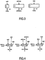
- FIG. 3 illustrates a request queue stage which generally corresponds to a shift register stage, allowing to store the quantities web 43, address 45, and data 47.
- Load/store operations have not been shown in particular in this Figure. In general, they can be effected in either of two modes. In the short latency mode, load/store operations will only experience the intrinsic memory latency L1 of the memory that may, for example, be an SRAM. Then, each memory bank conflict will result in a stall cycle. In the long latency mode however, a slack interval S is added to memory latency L1, so that load/store operations will experience an overall latency of (S + L1).
- the request queue embodiment selectively supports both latency modes by using a special bypass block 66. In the short latency mode, this block will be used to bypass all stages 64, thereby assigning to the actually incoming request the highest priority, whilst disabling all others.
- the associated latency mode signal has been labeled 67.
- Figure 4 illustrates a request queue bypass embodiment. It has been constructed from a set of multiplexers 66A, 66B, 66C, that will collectively select either the latest incoming request, or the request that is leaving the final queue stage S-1 . The actually selected request will have the highest priority.
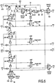
- Figure 5 illustrates a request queue controller embodiment, for realizing block 60 in Figure 2 .
- Acknowledge signal ack 0 arrives at top left and feeds AND gate 78, as well as after inversion in element 73, AND gate 72.
- the chip select cs signal feeds AND gates 72, 78, and 80, the latter furthermore receiving acknowledge signal ack S.
- the latter two AND gates feed selector 86, that is controlled by the long/short latency mode signal to select the input signal as indicated.
- the transmitted signal enters OR gate 88, and is selectively transmitted through selector 90, that is controlled by the stall signal as shown.
- the signal transferred is latched in latch 92, to operate as mask signal.
- the mask signal is furthermore retrocoupled to OR gate 88.
- the mask signal is inverted in inverter 96 and then fed to clocked AND gate 98.
- the output of AND gate 98 is fed to selector 100 which is controlled by the latency mode signal, so that the output of selector 100 will be either 0, or equal to the output signal of clocked AND gate 98.
- the inverted acknowledge ack 0 signal will be clocked to selector 84 that is controlled by the stall signal.
- the signal selected is fed to selector 94 that on its other input receives a 0 signal and is itself controlled by the stall signal, to on its output generating the stage valid signal 76, cf. Figure 2 .
- the output of selector 84 will be fed to latch 70.
- the latch content represents the request signal req 1, and is furthermore retrocoupled to selector 82 which on its other input receives a zero (0), and which selector is controlled by the signal ack 1 from the next lower stage.
- the chip select value cs travels through a dedicated one-bit shift register with stages like stage 70, which register thus contains all pending requests. Furthermore, a received acknowledgement signal like signal 63A will clear the chip select signal cs at the stage in question through inverting an input to an AND gate like 72. Furthermore, from every chip select pipeline stage a valid flag like flag 76 is derived that drives the associated clock gate 62 in Figure 2 . The register will keep shifting as long as no memory bank conflicts will occur in the memory, that is, as long as no request queue gets full. (65) A conflict will however automatically cause a stall cycle, that stops the shifting of the queue. While the queue remains stalled, memory bank conflicts may get resolved, which means that actual requests will still be acknowledged. Hence, the clearing of acknowledged requests will continue during the stall interval.
- the final stage S has the request controlled in an inverse manner with respect to the other stages. Furthermore, the final stage S comprises AND gate 102 that corresponds to AND gates 72 of earlier stages, and also a second AND gate 104 that receives the inverted value of acknowledge signal ack S, and furthermore the inverted mask signal from latch 92.
- the two AND gates feed a selector 106 that is controlled by the latency mode control signal and transmits the full signal. When a request that had caused a queue to raise its full flag is acknowledged in this manner (without occurrence of a further full signal), the stalling signal from OR 65A is automatically terminated.
- a bypass element 66 controlled by the latency mode signal 67 is also visible.
- the entire queue will be bypassed, to assign the highest priority to the latest incoming request, whilst coincidently therewith, blocking all other requests.
- the latency mode signal 67 may be given by an operator and/or by the system, such as being based on statistical and/or dynamic data. A longer latency, even caused by only a single stage, will dramatically decrease the number of conflicts, and thereby, the number of delaying stalls. However, a longer latency will also present a longer delay.
- the system should be controlled by the best trade-off that were relevant for the application or application interval in question.
- Figure 6 illustrates a request routing facility from the request queues to the memory bank arbiters.
- This combinatory network routes all requests from all request queues to the appropriate memory bank arbiter (36-40 in Figure 1 ), and would route acknowledgements pertaining to these requests back to the associated request queue, the latter not having been shown in Figure 6 .
- the memory map is uniformly interleaved over the various memory banks, the specific bank in question is determined as based on examining the least significant bits associated with the relevant access request signals. The latter is effected by bit select items like 69. The result of this bit select operation controls a demultiplexer-like item 70 that will in consequence route a one-bit request flag to the intended memory bank arbiter such as items 36-40.
- the components web, address, and data of the request are directly forwarded to all bank arbiters in parallel on an interconnection shown in bold representation.
- the total number of request lines arriving at every bank arbiter then equals the number of request queues times the maximum number of requests generated by each request queue. With a slack S, this number is (S + 1) *L.
- each request may only be acknowledged by one single bank arbiter. Therefore, for each particular request, an ORING in elements 37, 39, 41 of all corresponding acknowledge flags from the respective arbiters 36-40 will yield the associated acknowledge value.
- Figure 7 illustrates this acknowledgement routing facility from the various memory bank arbiters to the pertinent request queues.
- Figure 8 illustrates a bank arbiter embodiment.
- the bank arbiter is operative for selecting the highest priority request presented to its input, for acknowledging this request, and for forwarding the information associated with the request to the memory bank in question.
- the incoming request flags are considered as a sorted bit vector with the relatively higher priority request flags as most significant bits, and the relatively lower priority request flags as least significant bits.
- the arbiter will search for the bit with the highest significance level in this vector that is "1". This bit corresponds to the valid request with the highest priority.
- the index of the bit in question is used to select the request that must be acknowledged. It also indicates the load/store unit from which the request is coming. This latter information will send load data for a read access back to the proper load/store unit. To have this information available at the instant on which the loaded data is available for reading, the index is sent to the intermediate queue, through which it travels to stay in synchronism with the data to be read from the addressed memory bank.
- the arbiter facility comprises selector facilities like 120 and 122.
- Selector facility 120 is controlled at the left side by the various requests ranging from (LSU L-1, row S), to (LSU 0, row 0). Furthermore, the selector facility 120 receives at the upper side the web, address, data, abd Isu id signals, and furthermore a signal def, or 0. As shown, the priorities have a leading string of 0,.... zeroes, then a first "1" at mutually exclusive positions, followed by string that may have any appropriate value. The selector will output the selected request, web, address, data, Isu id, and remaining slack signals.
- a second selector facility 122 is controlled by the same control signals at the left hand side as earlier, and receives at the various top bit strings with a single "1" at mutually exclusive positions, and furthermore exclusively zeroes.
- the selector will output acknowledge signals ranging from (LSU L-1, row S), to (LSU 0, row 0).
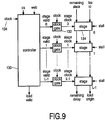
- FIG. 9 illustrates an intermediate queue embodiment.
- the intermediate queue is therefore used as a delay line for synchronizing the information pertaining to a load access during the interval in which the actual SRAM in the data memory is accessed. It consists of a single controller 130 and a number of stages such as stage 134, the number thereof being equal to the latency L1 of the SRAM.
- the controller is clocked by the master clock 134 and will therefore always be active: it will produce a number of L1 stage valid flags that control one clock gate such as gate 132 for each stage.
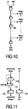
- Figure 10 illustrates an intermediate queue controller embodiment. It consists of a single-bit-wide delay line with stages like latch 136, which is serially fed by the signals cs and web, and which holds the valid flags for the various stages. Each such flag signifies a load operation and is created by ANDING the chip select and low-active write enable input signals. The serial output signal is load valid.
- FIG 11 illustrates an intermediate queue stage.
- Each stage has two registers, a first one (140) for holding an identifier to identify the load/store unit that issued the load request, and another one (138) to hold the remaining delay value, thereby indicating how much slack the request still will have to undergo in the data memory to meet the intended load/store latency interval. If a conflict occurs in the memory that leads to a processor stall, processor cycle time will be halted. To keep the remaining delay value consistent with processor cycle time, the value in this case will be incremented in incrementing element 142; the pertinent selection is executed through selector 144 that is controlled by the stall signal.
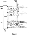
- Figure 12 illustrates a result queue embodiment, here consisting of a single controller 146 and a plurality of stages like stage 150, the number of these stages is a function of the slack, the memory latency times and the number of load/store units minus 1.
- the number of stages is approximately equal to MAX (S , L *(LSU - 1).
- the controller is clocked by the master clock and therefore, always active. It produces S stage valid flags that control S clock gates like clock gate 148, one for every stage. As a result, the stage is only active when it stores valid data, again for diminishing the level of power consumption.
- a result queue will collect and buffer the data and other informations coming out of its corresponding SRAM and out of the intermediate queue to perform the final synchronization with the processor core.
- the signals load valid, load data, load/store unit identifier, and remaining delay will successively enter the queue in stage 150 at its top as shown. Once in the queue, the result as loaded undergoes its final delay. Once the remaining delay of a result reaches the value zero, the result is issued as a valid result at one of the stage outputs of the relevant queue. Multiple results that are intended for respective different load/store units can leave the queue in parallel.
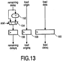
- Figure 13 illustrates a result queue stage embodiment that consists or three registers that respectively hold the remaining delay value (register 156), the data (register 160), and the load/store unit identifier of a load operation (register 158). All stages taken together constitute a shift register.
- the remaining delay value is decremented in each stage (element 152), so that with the traversing of successive stages the remaining delay will eventually reach zero, to indicate that the total load/store latency has been attained. At that instant, the result may be sent back to the load/store unit. If a conflict occurs in memory that leads to a processor stall, the processor cycle time will be standing still. To keep the remaining delay value synchronized with the processor cycle time count, the remaining delay value is kept constant in this case through circumventing decrementer stage 152 and appropriate control of selector 154.
- Figure 14 illustrates a result queue controller embodiment, thereby realizing a delay line for producing stage valid flags for the clock gates that control the various stages.
- the remaining delay value is examined. Once this value attains zero, the stage valid flag in this stage is cleared. Note also that if the processor is stalled by a memory conflict, no result can be sent back, since no load/store unit will be able to receive it. Therefore, in this case the result valid flags are cleared.
- Each stage in this controller comprises the following items, that are referred by number only in the first stage. First, the remaining delay value is entered into decrementing element 162.
- the output thereof which equals the ORed value of all bits of the delay value, is fed to AND gate 164, together with the load valid signal in a serial arrangement across all stages.
- the output of the AND gate is fed to a selector 172 that is controlled by the stall signal.
- the output of the selector is latched in element 174, and thereupon fed to the next serial stage.
- the reducing element output is inverted in item 166, and likewise ANDED with the load valid signal in AND gate 168.
- the output value of this gate is fed to selector 170 which furthermore receives a "0" signal and which is controlled by the stall signal.
- the output signal of the selector 170 may yield the result valid 0 signal.
- the difference in the ultimate stage relates to the leaving out of items 164, 172 and associated wiring.
- Figure 15 illustrates a result router embodiment.
- This router executes sending the valid results that leave the result queue, back to the load/store units 162-164 from which the relevant requests did originate.
- the load/store unit id is used to determine the target load/store unit.
- a demultiplexer 180-184 selects the proper load/store unit whereto a valid flag should be sent. Since it is certain that in each cycle at most one valid request is sent back to a particular load/store unit, the result data to be sent back are determined by first bit-wise ANDING all result data with their corresponding result flag in two-input AND gates like 174-178, and next ORING them in OR gates 168-172 for each particular router.
Landscapes
- Engineering & Computer Science (AREA)
- Theoretical Computer Science (AREA)
- Physics & Mathematics (AREA)
- General Engineering & Computer Science (AREA)
- General Physics & Mathematics (AREA)
- Multi Processors (AREA)
- Executing Machine-Instructions (AREA)
- Measurement And Recording Of Electrical Phenomena And Electrical Characteristics Of The Living Body (AREA)
- Data Exchanges In Wide-Area Networks (AREA)
Claims (5)
- Eine Computerspeicheranordnung, die eine erste Mehrzahl (L) von Eingabeporteinrichtungen umfasst, die kollektiv durch eine erste Routereinrichtung (32) gekoppelt sind, um eine zweite Mehrzahl (B) von Speichermodulen selektiv zu speisen, von denen jedes eine jeweilige Speicherbank (20, 22, 24) umfasst, und die ferner eine Ausgabeporteinrichtung umfasst, die die kollektiv durch die zweite Mehrzahl von Speichermodulen gespeist wird, wobei die Computerspeicheranordnung eine Detektionseinrichtung zum Detektieren gleichzeitiger und kollidierender Zugriffe durch mehr als eine der ersten Mehrzahl von Eingabeporteinrichtungen umfasst, wobei die Computerspeicheranordnung Anforderungswarteschlangen (42, 44, 46) umfasst, um dadurch ein zusätzliches Verzögerungsintervall vorzusehen, wobei jede Anforderungswarteschlange (42) eine Mehrzahl von Stufen (64) umfasst, und eine jeweilige Entscheidungseinheit (36, 38, 40) umfasst, die wirksam ist, beim Auffinden von mehreren gleichzeitig ablaufenden Zugriffsanforderungen zum Zugriff auf eine entsprechende Speicherbank ein Entscheidungssignal (63) zu erzeugen, das eine bestimmte unter den gleichzeitig ablaufenden Zugriffsanforderungen zu deren ausschließlicher Bearbeitung unter Bevorzugung gegenüber weiteren Zugriffsanforderungen herausgreift, und die wirksam ist, solche weiteren Zugriffsanforderungen in die fragliche Anforderungswarteschlange einzureihen, während sie ein Haltesignal (stall) zum Signalisieren eines vorgeschriebenen Haltezyklus an eine Anforderungsquelle erzeugt, das dafür eine Zugriffslatenz impliziert, dadurch gekennzeichnet, dass jede der Anforderungswarteschlangen (42, 44, 46) eine dazugehörige entsprechende Eingabeporteinrichtung an den ersten Router (32) koppelt, und wobei aus jeder Anforderungswarteschlangenstufe (64) ein Speicherbank-Anforderungssignal 61 parallel ausgegeben werden kann, und jede der Anforderungswarteschlagen einen Umgehungsblock (66) aufweist, um in einem Kurzlatenz-Modus alle Stufen der Anforderungswarteschlange zu umgehen, um somit ein Verzögerungsintervall vorzusehen, das eine programmierbare Länge aufweist, um dadurch eine programmierbare Zugriffslatenz auszuwählen, während die Detektionseinrichtung zum Signalisieren des Haltesignals ausschließlich unter der Kontrolle einer vollständigen ODER-Signalisierung irgendeiner derartigen Anforderungswarteschlange wirksam ist.
- Eine Computerspeicheranordnung nach Anspruch 1, wobei die Zugriffslatenz einen ersten und einen zweiten programmierbaren Wert aufweist, und wobei der zweite programmierbare Wert im Wesentlichen Null ist.
- Eine Computerspeicheranordnung nach Anspruch 1, wobei die Ausgabeporteinrichtungen eine dritte Mehrzahl von Ausgabeports umfassen, die durch eine zweite Routereinrichtung (34) von der zweiten Mehrzahl von Speichermodulen (20, 22, 24) gespeist werden, wobei die erste Mehrzahl gleich der dritten Mehrzahl ist, jede Eingabeporteinrichtung mit einer jeweiligen Ausgabeporteinrichtung assoziiert ist, und jedes derartige Speichermodul eine jeweilige Ergebniswarteschlangeneinrichtung (48, 50, 52) für die Übergangsspeicherung eines Ergebniswertes umfasst, der aus der assoziierten Speicherbank ausgelesen wird.
- Eine Computerspeicheranordnung nach Anspruch 3, wobei ein solches Haltesignal (stall) für alle Eingabeporteinrichtungen parallel ausgegeben wird, und die programmierbaren Zugriffslatenzen unter den jeweiligen Anforderungswarteschlagen durch die Kombination von Anforderungswarteschlange (42, 44, 46) und assoziierter Ergebniswarteschlange (48, 50, 52) dadurch einheitlich sind, dass in der assoziierten Ergebniswarteschlange eine Zusatzverzögerung hinzugefügt wird, und eine derartige Programmierbarkeit durch eine selektiv aktivierte Umgehungseinrichtung (66) realisiert wird.
- Eine Computeranordnung, die eine vierte Mehrzahl von Lade-/Speichereinheiten (17, 18, 19) umfasst, die mit einer Computerspeicheranordnung nach Anspruch 1 verbunden sind, wobei die Anzahl der Eingabeporteinrichtungen in der ersten Mehrzahl und die Anzahl von Lade-/Speichereinheiten in der vierten Mehrzahl gleich sind.
Priority Applications (1)
| Application Number | Priority Date | Filing Date | Title |
|---|---|---|---|
| EP03725527A EP1512078B1 (de) | 2002-05-24 | 2003-05-22 | Programmierbare zugriffslatenzzeit in einem pseudo-multiportspeicher |
Applications Claiming Priority (4)
| Application Number | Priority Date | Filing Date | Title |
|---|---|---|---|
| EP02077041 | 2002-05-24 | ||
| EP02077041 | 2002-05-24 | ||
| PCT/IB2003/002194 WO2003100618A2 (en) | 2002-05-24 | 2003-05-22 | Programmed access latency in mock multiport memory |
| EP03725527A EP1512078B1 (de) | 2002-05-24 | 2003-05-22 | Programmierbare zugriffslatenzzeit in einem pseudo-multiportspeicher |
Publications (2)
| Publication Number | Publication Date |
|---|---|
| EP1512078A2 EP1512078A2 (de) | 2005-03-09 |
| EP1512078B1 true EP1512078B1 (de) | 2012-04-11 |
Family
ID=29558362
Family Applications (1)
| Application Number | Title | Priority Date | Filing Date |
|---|---|---|---|
| EP03725527A Expired - Lifetime EP1512078B1 (de) | 2002-05-24 | 2003-05-22 | Programmierbare zugriffslatenzzeit in einem pseudo-multiportspeicher |
Country Status (7)
| Country | Link |
|---|---|
| US (1) | US7231478B2 (de) |
| EP (1) | EP1512078B1 (de) |
| JP (1) | JP4566738B2 (de) |
| CN (1) | CN100350401C (de) |
| AT (1) | ATE553435T1 (de) |
| AU (1) | AU2003228058A1 (de) |
| WO (1) | WO2003100618A2 (de) |
Families Citing this family (24)
| Publication number | Priority date | Publication date | Assignee | Title |
|---|---|---|---|---|
| US7624172B1 (en) | 2000-03-17 | 2009-11-24 | Aol Llc | State change alerts mechanism |
| US9246975B2 (en) | 2000-03-17 | 2016-01-26 | Facebook, Inc. | State change alerts mechanism |
| US7716287B2 (en) * | 2004-03-05 | 2010-05-11 | Aol Inc. | Organizing entries in participant lists based on communications strengths |
| US8005919B2 (en) | 2002-11-18 | 2011-08-23 | Aol Inc. | Host-based intelligent results related to a character stream |
| US8122137B2 (en) | 2002-11-18 | 2012-02-21 | Aol Inc. | Dynamic location of a subordinate user |
| US7428580B2 (en) | 2003-11-26 | 2008-09-23 | Aol Llc | Electronic message forwarding |
| AU2003287671A1 (en) | 2002-11-18 | 2004-06-15 | America Online, Inc. | People lists |
| US7590696B1 (en) | 2002-11-18 | 2009-09-15 | Aol Llc | Enhanced buddy list using mobile device identifiers |
| US7640306B2 (en) | 2002-11-18 | 2009-12-29 | Aol Llc | Reconfiguring an electronic message to effect an enhanced notification |
| US7899862B2 (en) | 2002-11-18 | 2011-03-01 | Aol Inc. | Dynamic identification of other users to an online user |
| US8701014B1 (en) | 2002-11-18 | 2014-04-15 | Facebook, Inc. | Account linking |
| US20040205127A1 (en) | 2003-03-26 | 2004-10-14 | Roy Ben-Yoseph | Identifying and using identities deemed to be known to a user |
| US7653693B2 (en) | 2003-09-05 | 2010-01-26 | Aol Llc | Method and system for capturing instant messages |
| US8560795B2 (en) * | 2005-06-30 | 2013-10-15 | Imec | Memory arrangement for multi-processor systems including a memory queue |
| ATE520086T1 (de) * | 2005-06-30 | 2011-08-15 | Imec | Speicheranordnung für mehrprozessorsysteme |
| EP1955175A1 (de) * | 2005-09-09 | 2008-08-13 | Freescale Semiconductor, Inc. | Verbindungseinrichtung und verfahren zum entwurf einer verbindungseinrichtung |
| EP2132630A1 (de) * | 2007-03-28 | 2009-12-16 | Nxp B.V. | Mehrfachverarbeitungssystem und verfahren |
| CN102799549A (zh) * | 2011-05-23 | 2012-11-28 | 中兴通讯股份有限公司 | 一种多源端口的数据处理方法及装置 |
| KR101862799B1 (ko) | 2011-12-12 | 2018-05-31 | 삼성전자주식회사 | 메모리 컨트롤러 및 메모리 컨트롤 방법 |
| US9934043B2 (en) * | 2013-08-08 | 2018-04-03 | Linear Algebra Technologies Limited | Apparatus, systems, and methods for providing computational imaging pipeline |
| US9940264B2 (en) * | 2014-10-10 | 2018-04-10 | International Business Machines Corporation | Load and store ordering for a strongly ordered simultaneous multithreading core |
| CN105701040B (zh) * | 2014-11-28 | 2018-12-07 | 杭州华为数字技术有限公司 | 一种激活内存的方法及装置 |
| US11216212B2 (en) * | 2019-03-19 | 2022-01-04 | International Business Machines Corporation | Minimizing conflicts in multiport banked memory arrays |
| CN112231254B (zh) * | 2020-09-22 | 2022-04-26 | 深圳云天励飞技术股份有限公司 | 存储器仲裁方法及存储器控制器 |
Family Cites Families (20)
| Publication number | Priority date | Publication date | Assignee | Title |
|---|---|---|---|---|
| US4564943A (en) * | 1983-07-05 | 1986-01-14 | International Business Machines | System path stressing |
| JPH0628051B2 (ja) * | 1986-04-25 | 1994-04-13 | 株式会社日立製作所 | 記憶制御方式 |
| US5142638A (en) * | 1989-02-07 | 1992-08-25 | Cray Research, Inc. | Apparatus for sharing memory in a multiprocessor system |
| US5280608A (en) * | 1991-06-28 | 1994-01-18 | Digital Equipment Corporation | Programmable stall cycles |
| US5440713A (en) * | 1992-05-29 | 1995-08-08 | Industrial Technology Research Institute | M-way N-port paged-interleaved memory system |
| US5710912A (en) * | 1993-05-06 | 1998-01-20 | Hewlett-Packard Co. | Method and apparatus for enabling a computer system to adjust for latency assumptions |
| JPH06314264A (ja) * | 1993-05-06 | 1994-11-08 | Nec Corp | セルフ・ルーティング・クロスバー・スイッチ |
| JP3199207B2 (ja) * | 1993-12-16 | 2001-08-13 | シャープ株式会社 | マルチポート半導体記憶装置 |
| US5701434A (en) * | 1995-03-16 | 1997-12-23 | Hitachi, Ltd. | Interleave memory controller with a common access queue |
| JP2882304B2 (ja) * | 1995-03-22 | 1999-04-12 | 日本電気株式会社 | マルチプロセッサシステム |
| US6212607B1 (en) * | 1997-01-17 | 2001-04-03 | Integrated Device Technology, Inc. | Multi-ported memory architecture using single-ported RAM |
| US6006296A (en) * | 1997-05-16 | 1999-12-21 | Unisys Corporation | Scalable memory controller |
| US6067606A (en) * | 1997-12-15 | 2000-05-23 | Intel Corporation | Computer processor with dynamic setting of latency values for memory access |
| US6618777B1 (en) * | 1999-01-21 | 2003-09-09 | Analog Devices, Inc. | Method and apparatus for communicating between multiple functional units in a computer environment |
| US6393512B1 (en) * | 1999-09-27 | 2002-05-21 | Ati International Srl | Circuit and method for detecting bank conflicts in accessing adjacent banks |
| US6738386B1 (en) * | 2000-05-11 | 2004-05-18 | Agere Systems Inc. | Controlled latency with dynamically limited queue depth based on history and latency estimation |
| US6477598B1 (en) * | 2000-07-20 | 2002-11-05 | Lsi Logic Corporation | Memory controller arbitrating RAS, CAS and bank precharge signals |
| JP2002055879A (ja) * | 2000-08-11 | 2002-02-20 | Univ Hiroshima | マルチポートキャッシュメモリ |
| US6782441B1 (en) * | 2000-10-26 | 2004-08-24 | Sun Microsystems, Inc. | Arbitration method and apparatus |
| US6970454B1 (en) * | 2001-08-09 | 2005-11-29 | Pasternak Solutions Llc | Sliced crossbar architecture with inter-slice communication |
-
2003
- 2003-05-22 US US10/515,463 patent/US7231478B2/en not_active Expired - Fee Related
- 2003-05-22 AT AT03725527T patent/ATE553435T1/de active
- 2003-05-22 EP EP03725527A patent/EP1512078B1/de not_active Expired - Lifetime
- 2003-05-22 WO PCT/IB2003/002194 patent/WO2003100618A2/en not_active Ceased
- 2003-05-22 JP JP2004508003A patent/JP4566738B2/ja not_active Expired - Fee Related
- 2003-05-22 CN CNB038117665A patent/CN100350401C/zh not_active Expired - Fee Related
- 2003-05-22 AU AU2003228058A patent/AU2003228058A1/en not_active Abandoned
Also Published As
| Publication number | Publication date |
|---|---|
| WO2003100618A3 (en) | 2004-09-10 |
| JP4566738B2 (ja) | 2010-10-20 |
| AU2003228058A8 (en) | 2003-12-12 |
| US7231478B2 (en) | 2007-06-12 |
| EP1512078A2 (de) | 2005-03-09 |
| ATE553435T1 (de) | 2012-04-15 |
| CN100350401C (zh) | 2007-11-21 |
| JP2005527040A (ja) | 2005-09-08 |
| AU2003228058A1 (en) | 2003-12-12 |
| CN1656461A (zh) | 2005-08-17 |
| WO2003100618A2 (en) | 2003-12-04 |
| US20050177689A1 (en) | 2005-08-11 |
Similar Documents
| Publication | Publication Date | Title |
|---|---|---|
| EP1512078B1 (de) | Programmierbare zugriffslatenzzeit in einem pseudo-multiportspeicher | |
| US7047370B1 (en) | Full access to memory interfaces via remote request | |
| US5740402A (en) | Conflict resolution in interleaved memory systems with multiple parallel accesses | |
| US4750154A (en) | Memory alignment system and method | |
| US6925520B2 (en) | Self-optimizing crossbar switch | |
| KR100321784B1 (ko) | 중재 지연 내성의 분산형 입력 버퍼 스위치 시스템 및그를 이용한 입력 데이터 처리 방법 | |
| US5446844A (en) | Peripheral memory interface controller as a cache for a large data processing system | |
| EP1512079B1 (de) | Pseudo-multiport datenspeicher mit haltfunktion | |
| WO2004099995A2 (en) | Hierarchical memory access via pipelining | |
| US7155540B2 (en) | Data communication method in shared memory multiprocessor system | |
| JP2644185B2 (ja) | データ処理装置 | |
| US6145032A (en) | System for recirculation of communication transactions in data processing in the event of communication stall | |
| US8713216B2 (en) | Processor and data transfer method | |
| US20080320185A1 (en) | Buffering device and buffering method | |
| WO2006124460A2 (en) | Concurrent read response acknowledge enhanced direct memory access unit | |
| JP2882304B2 (ja) | マルチプロセッサシステム | |
| US6055607A (en) | Interface queue with bypassing capability for main storage unit | |
| US20040111567A1 (en) | SIMD processor with multi-port memory unit | |
| JP3982077B2 (ja) | マルチプロセッサシステム | |
| JPH02294755A (ja) | データ処理装置 | |
| JPH09269937A (ja) | プロセッサ間通信におけるパケット送信方法およびその装置 | |
| WO2004051498A2 (en) | A simd processor with multi-port memory unit | |
| JP2731743B2 (ja) | 通信レジスタ付並列計算機 | |
| JPH1091589A (ja) | プロセッサ間同期制御装置 | |
| JP4306997B2 (ja) | データ制御装置及びatm制御装置 |
Legal Events
| Date | Code | Title | Description |
|---|---|---|---|
| PUAI | Public reference made under article 153(3) epc to a published international application that has entered the european phase |
Free format text: ORIGINAL CODE: 0009012 |
|
| AK | Designated contracting states |
Kind code of ref document: A2 Designated state(s): AT BE BG CH CY CZ DE DK EE ES FI FR GB GR HU IE IT LI LU MC NL PT RO SE SI SK TR |
|
| 17P | Request for examination filed |
Effective date: 20050310 |
|
| RAP1 | Party data changed (applicant data changed or rights of an application transferred) |
Owner name: SILICON HIVE B.V. |
|
| RAP1 | Party data changed (applicant data changed or rights of an application transferred) |
Owner name: SILICON HIVE B.V. |
|
| 17Q | First examination report despatched |
Effective date: 20110302 |
|
| GRAP | Despatch of communication of intention to grant a patent |
Free format text: ORIGINAL CODE: EPIDOSNIGR1 |
|
| GRAS | Grant fee paid |
Free format text: ORIGINAL CODE: EPIDOSNIGR3 |
|
| GRAA | (expected) grant |
Free format text: ORIGINAL CODE: 0009210 |
|
| AK | Designated contracting states |
Kind code of ref document: B1 Designated state(s): AT BE BG CH CY CZ DE DK EE ES FI FR GB GR HU IE IT LI LU MC NL PT RO SE SI SK TR |
|
| REG | Reference to a national code |
Ref country code: GB Ref legal event code: FG4D |
|
| REG | Reference to a national code |
Ref country code: CH Ref legal event code: EP |
|
| REG | Reference to a national code |
Ref country code: AT Ref legal event code: REF Ref document number: 553435 Country of ref document: AT Kind code of ref document: T Effective date: 20120415 |
|
| REG | Reference to a national code |
Ref country code: IE Ref legal event code: FG4D |
|
| REG | Reference to a national code |
Ref country code: DE Ref legal event code: R096 Ref document number: 60340567 Country of ref document: DE Effective date: 20120606 |
|
| REG | Reference to a national code |
Ref country code: NL Ref legal event code: VDEP Effective date: 20120411 |
|
| REG | Reference to a national code |
Ref country code: AT Ref legal event code: MK05 Ref document number: 553435 Country of ref document: AT Kind code of ref document: T Effective date: 20120411 |
|
| PG25 | Lapsed in a contracting state [announced via postgrant information from national office to epo] |
Ref country code: SE Free format text: LAPSE BECAUSE OF FAILURE TO SUBMIT A TRANSLATION OF THE DESCRIPTION OR TO PAY THE FEE WITHIN THE PRESCRIBED TIME-LIMIT Effective date: 20120411 Ref country code: FI Free format text: LAPSE BECAUSE OF FAILURE TO SUBMIT A TRANSLATION OF THE DESCRIPTION OR TO PAY THE FEE WITHIN THE PRESCRIBED TIME-LIMIT Effective date: 20120411 Ref country code: CY Free format text: LAPSE BECAUSE OF FAILURE TO SUBMIT A TRANSLATION OF THE DESCRIPTION OR TO PAY THE FEE WITHIN THE PRESCRIBED TIME-LIMIT Effective date: 20120411 |
|
| PG25 | Lapsed in a contracting state [announced via postgrant information from national office to epo] |
Ref country code: PT Free format text: LAPSE BECAUSE OF FAILURE TO SUBMIT A TRANSLATION OF THE DESCRIPTION OR TO PAY THE FEE WITHIN THE PRESCRIBED TIME-LIMIT Effective date: 20120813 Ref country code: GR Free format text: LAPSE BECAUSE OF FAILURE TO SUBMIT A TRANSLATION OF THE DESCRIPTION OR TO PAY THE FEE WITHIN THE PRESCRIBED TIME-LIMIT Effective date: 20120712 Ref country code: SI Free format text: LAPSE BECAUSE OF FAILURE TO SUBMIT A TRANSLATION OF THE DESCRIPTION OR TO PAY THE FEE WITHIN THE PRESCRIBED TIME-LIMIT Effective date: 20120411 |
|
| PG25 | Lapsed in a contracting state [announced via postgrant information from national office to epo] |
Ref country code: MC Free format text: LAPSE BECAUSE OF NON-PAYMENT OF DUE FEES Effective date: 20120531 Ref country code: BE Free format text: LAPSE BECAUSE OF FAILURE TO SUBMIT A TRANSLATION OF THE DESCRIPTION OR TO PAY THE FEE WITHIN THE PRESCRIBED TIME-LIMIT Effective date: 20120411 |
|
| REG | Reference to a national code |
Ref country code: CH Ref legal event code: PL |
|
| PG25 | Lapsed in a contracting state [announced via postgrant information from national office to epo] |
Ref country code: LI Free format text: LAPSE BECAUSE OF NON-PAYMENT OF DUE FEES Effective date: 20120531 Ref country code: NL Free format text: LAPSE BECAUSE OF FAILURE TO SUBMIT A TRANSLATION OF THE DESCRIPTION OR TO PAY THE FEE WITHIN THE PRESCRIBED TIME-LIMIT Effective date: 20120411 Ref country code: EE Free format text: LAPSE BECAUSE OF FAILURE TO SUBMIT A TRANSLATION OF THE DESCRIPTION OR TO PAY THE FEE WITHIN THE PRESCRIBED TIME-LIMIT Effective date: 20120411 Ref country code: SK Free format text: LAPSE BECAUSE OF FAILURE TO SUBMIT A TRANSLATION OF THE DESCRIPTION OR TO PAY THE FEE WITHIN THE PRESCRIBED TIME-LIMIT Effective date: 20120411 Ref country code: CZ Free format text: LAPSE BECAUSE OF FAILURE TO SUBMIT A TRANSLATION OF THE DESCRIPTION OR TO PAY THE FEE WITHIN THE PRESCRIBED TIME-LIMIT Effective date: 20120411 Ref country code: CH Free format text: LAPSE BECAUSE OF NON-PAYMENT OF DUE FEES Effective date: 20120531 Ref country code: AT Free format text: LAPSE BECAUSE OF FAILURE TO SUBMIT A TRANSLATION OF THE DESCRIPTION OR TO PAY THE FEE WITHIN THE PRESCRIBED TIME-LIMIT Effective date: 20120411 Ref country code: RO Free format text: LAPSE BECAUSE OF FAILURE TO SUBMIT A TRANSLATION OF THE DESCRIPTION OR TO PAY THE FEE WITHIN THE PRESCRIBED TIME-LIMIT Effective date: 20120411 Ref country code: DK Free format text: LAPSE BECAUSE OF FAILURE TO SUBMIT A TRANSLATION OF THE DESCRIPTION OR TO PAY THE FEE WITHIN THE PRESCRIBED TIME-LIMIT Effective date: 20120411 |
|
| PLBE | No opposition filed within time limit |
Free format text: ORIGINAL CODE: 0009261 |
|
| STAA | Information on the status of an ep patent application or granted ep patent |
Free format text: STATUS: NO OPPOSITION FILED WITHIN TIME LIMIT |
|
| REG | Reference to a national code |
Ref country code: IE Ref legal event code: MM4A |
|
| PG25 | Lapsed in a contracting state [announced via postgrant information from national office to epo] |
Ref country code: IT Free format text: LAPSE BECAUSE OF FAILURE TO SUBMIT A TRANSLATION OF THE DESCRIPTION OR TO PAY THE FEE WITHIN THE PRESCRIBED TIME-LIMIT Effective date: 20120411 |
|
| REG | Reference to a national code |
Ref country code: FR Ref legal event code: ST Effective date: 20130131 |
|
| 26N | No opposition filed |
Effective date: 20130114 |
|
| PG25 | Lapsed in a contracting state [announced via postgrant information from national office to epo] |
Ref country code: IE Free format text: LAPSE BECAUSE OF NON-PAYMENT OF DUE FEES Effective date: 20120522 Ref country code: FR Free format text: LAPSE BECAUSE OF NON-PAYMENT OF DUE FEES Effective date: 20120611 Ref country code: ES Free format text: LAPSE BECAUSE OF FAILURE TO SUBMIT A TRANSLATION OF THE DESCRIPTION OR TO PAY THE FEE WITHIN THE PRESCRIBED TIME-LIMIT Effective date: 20120722 |
|
| REG | Reference to a national code |
Ref country code: DE Ref legal event code: R097 Ref document number: 60340567 Country of ref document: DE Effective date: 20130114 |
|
| PG25 | Lapsed in a contracting state [announced via postgrant information from national office to epo] |
Ref country code: BG Free format text: LAPSE BECAUSE OF FAILURE TO SUBMIT A TRANSLATION OF THE DESCRIPTION OR TO PAY THE FEE WITHIN THE PRESCRIBED TIME-LIMIT Effective date: 20120711 |
|
| REG | Reference to a national code |
Ref country code: GB Ref legal event code: 732E Free format text: REGISTERED BETWEEN 20140213 AND 20140219 |
|
| PG25 | Lapsed in a contracting state [announced via postgrant information from national office to epo] |
Ref country code: TR Free format text: LAPSE BECAUSE OF FAILURE TO SUBMIT A TRANSLATION OF THE DESCRIPTION OR TO PAY THE FEE WITHIN THE PRESCRIBED TIME-LIMIT Effective date: 20120411 |
|
| REG | Reference to a national code |
Ref country code: DE Ref legal event code: R081 Ref document number: 60340567 Country of ref document: DE Owner name: INTEL CORPORATION, US Free format text: FORMER OWNER: SILICON HIVE B. V., EINDHOVEN, NL Effective date: 20140417 Ref country code: DE Ref legal event code: R082 Ref document number: 60340567 Country of ref document: DE Representative=s name: VEREENIGDE OCTROOIBUREAUX V.O., DE Effective date: 20140417 Ref country code: DE Ref legal event code: R081 Ref document number: 60340567 Country of ref document: DE Owner name: INTEL CORPORATION, US Free format text: FORMER OWNER: KONINKLIJKE PHILIPS ELECTRONICS N.V., EINDHOVEN, NL Effective date: 20120412 Ref country code: DE Ref legal event code: R081 Ref document number: 60340567 Country of ref document: DE Owner name: INTEL CORPORATION, SANTA CLARA, US Free format text: FORMER OWNER: KONINKLIJKE PHILIPS ELECTRONICS N.V., EINDHOVEN, NL Effective date: 20120412 Ref country code: DE Ref legal event code: R081 Ref document number: 60340567 Country of ref document: DE Owner name: INTEL CORPORATION, SANTA CLARA, US Free format text: FORMER OWNER: SILICON HIVE B. V., EINDHOVEN, NL Effective date: 20140417 |
|
| PG25 | Lapsed in a contracting state [announced via postgrant information from national office to epo] |
Ref country code: LU Free format text: LAPSE BECAUSE OF NON-PAYMENT OF DUE FEES Effective date: 20120522 |
|
| PG25 | Lapsed in a contracting state [announced via postgrant information from national office to epo] |
Ref country code: HU Free format text: LAPSE BECAUSE OF FAILURE TO SUBMIT A TRANSLATION OF THE DESCRIPTION OR TO PAY THE FEE WITHIN THE PRESCRIBED TIME-LIMIT Effective date: 20030522 |
|
| PGFP | Annual fee paid to national office [announced via postgrant information from national office to epo] |
Ref country code: DE Payment date: 20200512 Year of fee payment: 18 |
|
| PGFP | Annual fee paid to national office [announced via postgrant information from national office to epo] |
Ref country code: GB Payment date: 20200513 Year of fee payment: 18 |
|
| REG | Reference to a national code |
Ref country code: DE Ref legal event code: R119 Ref document number: 60340567 Country of ref document: DE |
|
| GBPC | Gb: european patent ceased through non-payment of renewal fee |
Effective date: 20210522 |
|
| PG25 | Lapsed in a contracting state [announced via postgrant information from national office to epo] |
Ref country code: GB Free format text: LAPSE BECAUSE OF NON-PAYMENT OF DUE FEES Effective date: 20210522 Ref country code: DE Free format text: LAPSE BECAUSE OF NON-PAYMENT OF DUE FEES Effective date: 20211201 |