EP1517370A2 - Verfahren zur Herstellung gebondeter metallischer/keramischer Leiterplatten - Google Patents
Verfahren zur Herstellung gebondeter metallischer/keramischer Leiterplatten Download PDFInfo
- Publication number
- EP1517370A2 EP1517370A2 EP04022435A EP04022435A EP1517370A2 EP 1517370 A2 EP1517370 A2 EP 1517370A2 EP 04022435 A EP04022435 A EP 04022435A EP 04022435 A EP04022435 A EP 04022435A EP 1517370 A2 EP1517370 A2 EP 1517370A2
- Authority
- EP
- European Patent Office
- Prior art keywords
- metal
- ceramic substrate
- ceramic
- circuit
- circuit pattern
- Prior art date
- Legal status (The legal status is an assumption and is not a legal conclusion. Google has not performed a legal analysis and makes no representation as to the accuracy of the status listed.)
- Granted
Links
Images


Classifications
-
- H—ELECTRICITY
- H10—SEMICONDUCTOR DEVICES; ELECTRIC SOLID-STATE DEVICES NOT OTHERWISE PROVIDED FOR
- H10W—GENERIC PACKAGES, INTERCONNECTIONS, CONNECTORS OR OTHER CONSTRUCTIONAL DETAILS OF DEVICES COVERED BY CLASS H10
- H10W70/00—Package substrates; Interposers; Redistribution layers [RDL]
- H10W70/01—Manufacture or treatment
- H10W70/02—Manufacture or treatment of conductive package substrates serving as an interconnection, e.g. of metal plates
-
- H—ELECTRICITY
- H05—ELECTRIC TECHNIQUES NOT OTHERWISE PROVIDED FOR
- H05K—PRINTED CIRCUITS; CASINGS OR CONSTRUCTIONAL DETAILS OF ELECTRIC APPARATUS; MANUFACTURE OF ASSEMBLAGES OF ELECTRICAL COMPONENTS
- H05K3/00—Apparatus or processes for manufacturing printed circuits
- H05K3/10—Apparatus or processes for manufacturing printed circuits in which conductive material is applied to the insulating support in such a manner as to form the desired conductive pattern
- H05K3/101—Apparatus or processes for manufacturing printed circuits in which conductive material is applied to the insulating support in such a manner as to form the desired conductive pattern by casting or moulding of conductive material
-
- H—ELECTRICITY
- H10—SEMICONDUCTOR DEVICES; ELECTRIC SOLID-STATE DEVICES NOT OTHERWISE PROVIDED FOR
- H10W—GENERIC PACKAGES, INTERCONNECTIONS, CONNECTORS OR OTHER CONSTRUCTIONAL DETAILS OF DEVICES COVERED BY CLASS H10
- H10W40/00—Arrangements for thermal protection or thermal control
- H10W40/20—Arrangements for cooling
- H10W40/25—Arrangements for cooling characterised by their materials
- H10W40/255—Arrangements for cooling characterised by their materials having a laminate or multilayered structure, e.g. direct bond copper [DBC] ceramic substrates
-
- H—ELECTRICITY
- H05—ELECTRIC TECHNIQUES NOT OTHERWISE PROVIDED FOR
- H05K—PRINTED CIRCUITS; CASINGS OR CONSTRUCTIONAL DETAILS OF ELECTRIC APPARATUS; MANUFACTURE OF ASSEMBLAGES OF ELECTRICAL COMPONENTS
- H05K1/00—Printed circuits
- H05K1/02—Details
- H05K1/03—Use of materials for the substrate
- H05K1/0306—Inorganic insulating substrates, e.g. ceramic, glass
-
- H—ELECTRICITY
- H05—ELECTRIC TECHNIQUES NOT OTHERWISE PROVIDED FOR
- H05K—PRINTED CIRCUITS; CASINGS OR CONSTRUCTIONAL DETAILS OF ELECTRIC APPARATUS; MANUFACTURE OF ASSEMBLAGES OF ELECTRICAL COMPONENTS
- H05K2203/00—Indexing scheme relating to apparatus or processes for manufacturing printed circuits covered by H05K3/00
- H05K2203/01—Tools for processing; Objects used during processing
- H05K2203/0104—Tools for processing; Objects used during processing for patterning or coating
- H05K2203/0108—Male die used for patterning, punching or transferring
-
- H—ELECTRICITY
- H05—ELECTRIC TECHNIQUES NOT OTHERWISE PROVIDED FOR
- H05K—PRINTED CIRCUITS; CASINGS OR CONSTRUCTIONAL DETAILS OF ELECTRIC APPARATUS; MANUFACTURE OF ASSEMBLAGES OF ELECTRICAL COMPONENTS
- H05K2203/00—Indexing scheme relating to apparatus or processes for manufacturing printed circuits covered by H05K3/00
- H05K2203/12—Using specific substances
- H05K2203/128—Molten metals, e.g. casting thereof, or melting by heating and excluding molten solder
-
- H—ELECTRICITY
- H05—ELECTRIC TECHNIQUES NOT OTHERWISE PROVIDED FOR
- H05K—PRINTED CIRCUITS; CASINGS OR CONSTRUCTIONAL DETAILS OF ELECTRIC APPARATUS; MANUFACTURE OF ASSEMBLAGES OF ELECTRICAL COMPONENTS
- H05K2203/00—Indexing scheme relating to apparatus or processes for manufacturing printed circuits covered by H05K3/00
- H05K2203/14—Related to the order of processing steps
- H05K2203/1476—Same or similar kind of process performed in phases, e.g. coarse patterning followed by fine patterning
-
- H—ELECTRICITY
- H05—ELECTRIC TECHNIQUES NOT OTHERWISE PROVIDED FOR
- H05K—PRINTED CIRCUITS; CASINGS OR CONSTRUCTIONAL DETAILS OF ELECTRIC APPARATUS; MANUFACTURE OF ASSEMBLAGES OF ELECTRICAL COMPONENTS
- H05K3/00—Apparatus or processes for manufacturing printed circuits
- H05K3/02—Apparatus or processes for manufacturing printed circuits in which the conductive material is applied to the surface of the insulating support and is thereafter removed from such areas of the surface which are not intended for current conducting or shielding
- H05K3/06—Apparatus or processes for manufacturing printed circuits in which the conductive material is applied to the surface of the insulating support and is thereafter removed from such areas of the surface which are not intended for current conducting or shielding the conductive material being removed chemically or electrolytically, e.g. by photo-etch process
- H05K3/061—Etching masks
-
- Y—GENERAL TAGGING OF NEW TECHNOLOGICAL DEVELOPMENTS; GENERAL TAGGING OF CROSS-SECTIONAL TECHNOLOGIES SPANNING OVER SEVERAL SECTIONS OF THE IPC; TECHNICAL SUBJECTS COVERED BY FORMER USPC CROSS-REFERENCE ART COLLECTIONS [XRACs] AND DIGESTS
- Y10—TECHNICAL SUBJECTS COVERED BY FORMER USPC
- Y10T—TECHNICAL SUBJECTS COVERED BY FORMER US CLASSIFICATION
- Y10T29/00—Metal working
- Y10T29/49—Method of mechanical manufacture
- Y10T29/49002—Electrical device making
- Y10T29/49117—Conductor or circuit manufacturing
- Y10T29/49124—On flat or curved insulated base, e.g., printed circuit, etc.
- Y10T29/49126—Assembling bases
-
- Y—GENERAL TAGGING OF NEW TECHNOLOGICAL DEVELOPMENTS; GENERAL TAGGING OF CROSS-SECTIONAL TECHNOLOGIES SPANNING OVER SEVERAL SECTIONS OF THE IPC; TECHNICAL SUBJECTS COVERED BY FORMER USPC CROSS-REFERENCE ART COLLECTIONS [XRACs] AND DIGESTS
- Y10—TECHNICAL SUBJECTS COVERED BY FORMER USPC
- Y10T—TECHNICAL SUBJECTS COVERED BY FORMER US CLASSIFICATION
- Y10T29/00—Metal working
- Y10T29/49—Method of mechanical manufacture
- Y10T29/49002—Electrical device making
- Y10T29/49117—Conductor or circuit manufacturing
- Y10T29/49124—On flat or curved insulated base, e.g., printed circuit, etc.
- Y10T29/49128—Assembling formed circuit to base
-
- Y—GENERAL TAGGING OF NEW TECHNOLOGICAL DEVELOPMENTS; GENERAL TAGGING OF CROSS-SECTIONAL TECHNOLOGIES SPANNING OVER SEVERAL SECTIONS OF THE IPC; TECHNICAL SUBJECTS COVERED BY FORMER USPC CROSS-REFERENCE ART COLLECTIONS [XRACs] AND DIGESTS
- Y10—TECHNICAL SUBJECTS COVERED BY FORMER USPC
- Y10T—TECHNICAL SUBJECTS COVERED BY FORMER US CLASSIFICATION
- Y10T29/00—Metal working
- Y10T29/49—Method of mechanical manufacture
- Y10T29/49002—Electrical device making
- Y10T29/49117—Conductor or circuit manufacturing
- Y10T29/49124—On flat or curved insulated base, e.g., printed circuit, etc.
- Y10T29/4913—Assembling to base an electrical component, e.g., capacitor, etc.
- Y10T29/49146—Assembling to base an electrical component, e.g., capacitor, etc. with encapsulating, e.g., potting, etc.
-
- Y—GENERAL TAGGING OF NEW TECHNOLOGICAL DEVELOPMENTS; GENERAL TAGGING OF CROSS-SECTIONAL TECHNOLOGIES SPANNING OVER SEVERAL SECTIONS OF THE IPC; TECHNICAL SUBJECTS COVERED BY FORMER USPC CROSS-REFERENCE ART COLLECTIONS [XRACs] AND DIGESTS
- Y10—TECHNICAL SUBJECTS COVERED BY FORMER USPC
- Y10T—TECHNICAL SUBJECTS COVERED BY FORMER US CLASSIFICATION
- Y10T29/00—Metal working
- Y10T29/49—Method of mechanical manufacture
- Y10T29/49002—Electrical device making
- Y10T29/49117—Conductor or circuit manufacturing
- Y10T29/49124—On flat or curved insulated base, e.g., printed circuit, etc.
- Y10T29/49155—Manufacturing circuit on or in base
- Y10T29/49156—Manufacturing circuit on or in base with selective destruction of conductive paths
Definitions
- the present invention generally relates to a method for producing a metal/ceramic bonding circuit board wherein a metal circuit plate is bonded to a ceramic substrate. More specifically, the invention relates to a method for producing a metal/ceramic bonding circuit board for use in a power module or the like.
- a method for producing a metal/ceramic bonding circuit board which has a metal circuit plate having a desired circuit pattern comprising the steps of: cooling and solidifying a molten metal, which is fed onto a ceramic substrate, to bond a metal plate to the ceramic substrate; printing an etching resist having a desired pattern shape on the bonded metal plate by the screen printing or the like; etching the metal plate to form a circuit pattern; and removing the resist (see, e.g., Japanese Patent Laid-Open No. 2002-76551).
- the thickness of a metal circuit plate is not less than hundreds micrometers, and is tens times as large as the thickness of a metal circuit plate of a printed circuit board usually using a paper or glass epoxy as an insulating material. Therefore, in the method disclosed in Japanese Patent Laid-Open No. 2002-76551, there is a problem in that the length of a skirt formed by etching and the amount of side etching caused by etching are large.
- the thickness of a metal circuit plate is in the range of from 0.4 mm to 0.6 mm and if an etching resist having a distance between patterns of 0.5 mm is formed, the insulating distance between patterns (the distance between bottoms) of the metal plate is a great distance of 0.9 to 1.4 mm at the shortest, and the distance between tops of metal circuit plates is greater than the distance between bottoms. If the metal circuit plate is thicker, there is a problem in that these distances are greater. In addition, as the thickness of the metal circuit plate increases, the time required to carry out etching increases, and the number of producing steps increases to increase production costs. Moreover, the resistance of the etching resist must be cared.
- a circuit forming metal plate is previously formed so as to have a shape similar to a circuit pattern by cooling and solidifying a molten metal contacting a ceramic substrate, it is possible to shorten the time required to carry out etching when a metal circuit plate having a desired circuit pattern is formed, and it is possible to form a fine pattern even if a circuit forming metal plate is thick.
- a method for producing a metal/ceramic bonding circuit board comprising the steps of: causing a molten metal to contact one side of a ceramic substrate; cooling and solidifying the molten metal contacting the one side of the ceramic substrate to bond a metal plate, which has a shape similar to a desired circuit pattern, to the one side of the ceramic substrate; and etching the metal plate to form a metal circuit plate having the desired circuit pattern.
- a portion of the metal plate, which is bonded to the one side of the ceramic substrate, other than a portion substantially corresponding to the desired circuit pattern is preferably thinner than the portion substantially corresponding to the desired circuit pattern.
- the portion of the metal plate, which is bonded to the one side of the ceramic substrate, other than a portion substantially corresponding to the desired circuit pattern preferably has a thickness which is half or less that of the portion substantially corresponding to the desired circuit pattern.
- the portion substantially corresponding to the desired circuit pattern preferably has a thickness of 0.1 to 0.3 mm.
- the ceramic substrate is preferably arranged in a mold which has a recessed portion having a shape similar to the desired circuit pattern, and the molten metal is preferably injected into the recessed portion of the mold so as to contact the one side of the ceramic substrate.
- the molten metal is preferably caused to contact the other side of the ceramic substrate at the step of causing the molten metal to contact the one side of the ceramic substrate, andametalmemberispreferably bonded to the other side of the ceramic substrate at the step of cooling and solidifying the molten metal contacting the one side of the ceramic substrate.
- the molten metal preferably contains aluminum as a principal component.
- a method for producing a metal/ceramic bonding circuit board comprising the steps of: preparing a mold having a recessed portion which has a shape similar to a desired circuit pattern; arranging a ceramic substrate in the mold so that the ceramic substrate is adjacent to the recessed portion; injecting a molten metal into the recessed portion of the mold so as to contact one side of the ceramic substrate arranged in the mold; cooling and solidifying the inj ected molten metal to bond a metal plate, which has a shape similar to the desired circuit pattern, to one side of the ceramic substrate; and etching the metal plate to form a metal circuit plate having the desired circuit pattern.
- a portion of the recessed portion of the mold other than a portion substantially corresponding to the desired circuit pattern is preferably shallower than the portion substantially corresponding to the desired circuit pattern.
- the portion substantially corresponding to the desired circuit pattern preferably has a depth of 0.1 to 0.3 mm.
- the molten metal is preferably caused to contact the other side of the ceramic substrate at the step of injecting the molten metal so as to contact the one side of the ceramic substrate, and a metal member ispreferably bonded to the other side of the ceramic substrate at the step of cooling and solidifying the molten metal to bond the metal plate to the one side of the ceramic substrate.
- the molten metal preferably contains aluminum as a principal component.
- the reason why the shape of a metal plate bonded to a ceramic substrate is a shape similar to a circuit pattern, not the same shape as the circuit pattern, is that it is difficult to form a metal plate having the same shape as that the circuit pattern at a predetermined dimensional precision when the metal plate bonded to the ceramic substrate is formedbymolding.
- a shape similar to a circuit pattern means a shape similar to a circuit pattern as similar as possible by molding.
- a metal plate is formed between adjacent patterns so as to be thin, it is possible to form a metal plate having a shape similar to a circuit pattern without forming each molten metal inlet in the mold for forming each circuit pattern.
- the present invention when a molten metal is caused to contact a ceramic substrate to be cooled and solidified to bond a circuit forming metal plate to the ceramic substrate to etch the circuit forming metal plate to form a metal circuit plate having a desired circuit pattern, if the circuit forming metal pattern bonded to the ceramic substrate is previously formed so as to have a shape similar to the circuit pattern, it is possible to form a fine pattern even if a circuit forming metal plate is thick, and it is possible to considerably shorten the time required to carry out etching for forming ametal circuit plate having a desired circuit pattern.
- a ceramic substrate is mounted in a mold, and a molten metal is fed into the mold to be cooled and solidified to produce a metal/ceramic bonding substrate wherein a metal base plate is bonded to one side of the ceramic substrate and a circuit forming metal plate is bonded to the other side thereof.
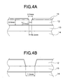
- FIGS. 1A through 1C show an example of a lower moldmember of a mold used for producing the metal/ ceramic bonding substrate.
- a lower mold member 100 comprises a bottom portion 100a having a substantially rectangular planar shape, and a side wall portion 100b extending from the peripheral edge portion of the bottom portion 100a upwards in a direction perpendicular to the bottom portion 100a.
- the top surface of the bottom portion 100a of the lower mold member 100 has one or a plurality of recessed portions 100c (two recessed portions 100c are shown in FIGS. 1A and 1B), each of which has a step-wise extending side wall.
- Each of the recessed portions 100c comprises: one or a plurality of metal circuit plate forming portions 100d (four metal circuit plate forming portions 100d are shown in FIGS. 1A and 1B) , each of which has a planer shape similar to a circuit pattern of a corresponding one of metal circuit plates and each of which substantially has the same depth as the thickness of the corresponding one of the metal circuit plates; and one or a plurality of ceramic substrate housing portions 100e (two ceramic substrate housing portions 100e are shown in FIGS. 1A and 1B) , each of which is formed above the metal circuit plate forming portions 100d so as to be adjacent thereto and each of which substantially has the same shape and size as those of the ceramic substrate. As shown in FIG.
- the depth of a portion between adjacent patterns is smaller than the depth of a portion, which substantially corresponds to the circuit pattern of the metal circuit plate, by d.
- a portion other than the recessed portions 100c of the lower mold member 100 defines a metal base plate forming portion 100f.
- the upper mold member has a molten metal inlet (not shown) for injecting a molten metal into the mold.
- the lower mold member 100 has a molten metal passage (not shown) , which extends between the metal base plate forming portion 100f and the metal circuit plate forming portions 100d, so as to allow the metal base plate forming portion 100f to be communicated with the metal circuit plate forming portions 100d if ceramic substrates are housed in the ceramic substrate housing portions 100e.
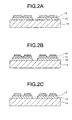
- a molten metal is injected into the metal base plate forming portion 100f to be filled in the metal circuit plate forming portions 100d via the molten metal passage (not shown) . Thereafter, the molten metal is cooled to be solidified, so that it is possible to produce an integrated metal/ceramic bonding substrate shown in FIG. 2A wherein a metal base plate 14 is bonded directly to one side of each of ceramic substrates 10, and circuit formingmetal plates 12 having a shape similar to a circuit pattern are bonded directly to the other side of the ceramic substrates 10.
- an etching resists 16 having a predetermined shape are printed on the surface of each of the circuit forming metal plates 12 to etch the circuit forming metal plates 12 with an etchant, such as a ferric chloride solution, to form metal circuit plates 12 having a desiredcircuitpattern.
- an etchant such as a ferric chloride solution
- the resists 16 are removed to obtain a metal/ceramic bonding circuit board having the metal circuit plates having the desired circuit pattern.
- a metal circuit plate forming portion being a recessed portion which substantially has the same shape and size as those of a circuit forming metal plate (see FIG. 3A) wherein the thickness of aportion substantially corresponding to a circuit pattern is 0.6 mm, the thickness of a portion between adjacent patterns is 0.3 mm, and the distance therebetween is 0.8 mm.
- a ceramic substrate housing portion being a recessed portion, which substantially has the same shape and size as those of a ceramic substrate having a size of 32.5 mm x 40 mm x 0. 635 mm, is formed above the metal circuit plate forming portion so as to be adjacent thereto.
- a metal base plate forming portion is defined above the ceramic substrate forming portion so as to be adjacent thereto.
- the carbon mold also has a molten metal passage extending between the metal base plate forming portion and the metal circuit plate forming portion.
- a ceramic substrate of aluminum nitride having a size of 32.5 mm x 40 mm x 0.635 mm was housed in the ceramic substrate housing portion of the lower mold member of the mold, and the lower mold member was closed by an upper mold member.
- a molten aluminum was fed from a molten metal inlet into the metal base plate forming portion to be filled in the metal circuit plate forming portion via the molten metal passage. Thereafter, the molten metal was cooled to be solidified to obtain an integrated metal/ceramic bonding substrate shown in FIG. 3A wherein a metal base plate 14 was bonded directly to one side of a ceramic substrate 10, and a circuit forming metal plate 12 having a shape similar to a circuit pattern was bonded directly to the other side of the ceramic substrate 10.
- etching resists 16 were printed on the surface of the circuit forming metal plate of the metal/ceramic bonding substrate so as to be spaced from each other by 1.2 mm between adjacent patterns. Then, the circuit forming metal plate was etched with a ferric chloride solution to form metal circuit plates having a desired circuit pattern. Thereafter, the etching resists 16 were removed to obtain a metal/ceramic bonding circuit board having the metal circuit plates having the desired circuit pattern wherein the distance (insulating distance) between pattern bottoms of adjacent patterns was 1.6 mm.
- Metal/ceramic bonding circuit boards were obtained by the same method as that in Example 1, except that the size of the ceramic substrate was 32.5 mm x 74 mm x 0.635 mm (Example 2), 32.5 mm x 40 mm x 0.25 mm (Example 3) and 32.5 mm x 74 mm x 0.25 mm (Example 4), respectively, and that the size of the ceramic substrate housing portion of the lower mold member was substantially equal to the size of the ceramic substrate.
- Metal/ceramic bonding circuit boards were obtained by the same methods as those in Examples 1 through 4, respectively, except that an alumina substrate was used as the ceramic substrate.
- Metal/ceramic bonding circuit boards were obtained by the same method as that in Example 9, except that the size of the ceramic substrate was 32.5 mm x 74 mm x 0.635 mm (Example 10), 32.5 mm x 40 mm x 0.25 mm (Example 11) and 32.5 mm x 74 mm x 0.25 mm (Example 12), respectively, and that the size of the ceramic substrate housing portion of the lower mold member was substantially equal to the size of the ceramic substrate.
- Metal/ceramic bonding circuit boards were obtained by the same methods as those in Examples 9 through 12, except that an alumina substrate was used as the ceramic substrate.
- Metal/ceramic bonding circuit boards were obtained by the same method as those in Examples 1 through 16, expect that the depth of the metal circuit plate forming portion was a constant depth of 0.6 mm.
Landscapes
- Engineering & Computer Science (AREA)
- Manufacturing & Machinery (AREA)
- Microelectronics & Electronic Packaging (AREA)
- Manufacturing Of Printed Circuit Boards (AREA)
- Insulated Metal Substrates For Printed Circuits (AREA)
Applications Claiming Priority (2)
| Application Number | Priority Date | Filing Date | Title |
|---|---|---|---|
| JP2003329278 | 2003-09-22 | ||
| JP2003329278A JP4441671B2 (ja) | 2003-09-22 | 2003-09-22 | 金属−セラミックス接合回路基板の製造方法 |
Publications (3)
| Publication Number | Publication Date |
|---|---|
| EP1517370A2 true EP1517370A2 (de) | 2005-03-23 |
| EP1517370A3 EP1517370A3 (de) | 2008-06-04 |
| EP1517370B1 EP1517370B1 (de) | 2016-12-14 |
Family
ID=34191415
Family Applications (1)
| Application Number | Title | Priority Date | Filing Date |
|---|---|---|---|
| EP04022435.4A Expired - Lifetime EP1517370B1 (de) | 2003-09-22 | 2004-09-21 | Verfahren zur Herstellung gebondeter metallischer/keramischer Leiterplatten |
Country Status (3)
| Country | Link |
|---|---|
| US (1) | US7340828B2 (de) |
| EP (1) | EP1517370B1 (de) |
| JP (1) | JP4441671B2 (de) |
Cited By (1)
| Publication number | Priority date | Publication date | Assignee | Title |
|---|---|---|---|---|
| TWI502709B (zh) * | 2011-08-26 | 2015-10-01 | 光頡科技股份有限公司 | Metallographic Ceramic Plate Method |
Families Citing this family (15)
| Publication number | Priority date | Publication date | Assignee | Title |
|---|---|---|---|---|
| JP4543279B2 (ja) * | 2004-03-31 | 2010-09-15 | Dowaメタルテック株式会社 | アルミニウム接合部材の製造方法 |
| JP5214546B2 (ja) * | 2009-07-01 | 2013-06-19 | Dowaメタルテック株式会社 | 端子付き金属−セラミックス回路基板の製造方法 |
| JP5554599B2 (ja) * | 2010-03-24 | 2014-07-23 | Dowaメタルテック株式会社 | 金属−セラミックス接合回路基板の製造方法 |
| JP5637719B2 (ja) * | 2010-03-31 | 2014-12-10 | Dowaメタルテック株式会社 | 金属セラミックス接合回路基板の製造方法 |
| CN103327735B (zh) * | 2013-06-04 | 2015-12-23 | 苏州晶品光电科技有限公司 | 高导热绝缘金属基印刷电路板 |
| CN103338588B (zh) * | 2013-06-04 | 2016-04-20 | 苏州晶品光电科技有限公司 | 高导热绝缘金属基印刷电路板 |
| CN103327736B (zh) * | 2013-06-04 | 2015-12-23 | 苏州晶品光电科技有限公司 | 高导热绝缘金属基印刷电路板 |
| CN103354220B (zh) * | 2013-06-17 | 2016-04-20 | 苏州晶品光电科技有限公司 | 用于光学和电子器件的图案化结构基板 |
| CN103354698B (zh) * | 2013-06-17 | 2016-02-24 | 苏州晶品光电科技有限公司 | 用于光学和电子器件的图案化陶瓷层印刷线路基板 |
| CN103354697B (zh) * | 2013-06-17 | 2016-04-20 | 苏州晶品光电科技有限公司 | 用于光学和电子器件的图案化复合陶瓷层印刷线路基板 |
| CN103354222B (zh) * | 2013-06-17 | 2016-01-13 | 苏州晶品光电科技有限公司 | 用于光学和电子器件的多层复合陶瓷层图案化结构基板 |
| JP6345957B2 (ja) * | 2014-03-24 | 2018-06-20 | Dowaメタルテック株式会社 | 金属−セラミックス回路基板およびその製造方法 |
| DE202014106063U1 (de) * | 2014-12-16 | 2015-02-12 | Danfoss Silicon Power Gmbh | Kühlwanne, Kühler und Leistungsmodulbaugruppe |
| JP6566586B2 (ja) * | 2018-04-11 | 2019-08-28 | Dowaメタルテック株式会社 | 金属−セラミックス回路基板およびその製造方法 |
| JP7157609B2 (ja) * | 2018-09-27 | 2022-10-20 | Dowaメタルテック株式会社 | 金属-セラミックス接合基板およびその製造方法 |
Family Cites Families (4)
| Publication number | Priority date | Publication date | Assignee | Title |
|---|---|---|---|---|
| JPS58180094A (ja) * | 1982-04-16 | 1983-10-21 | 株式会社日立製作所 | 多層プリント配線板の製造方法 |
| JPH03102892A (ja) * | 1989-09-18 | 1991-04-30 | Denki Kagaku Kogyo Kk | 回路基板の製造方法 |
| JP4756200B2 (ja) | 2000-09-04 | 2011-08-24 | Dowaメタルテック株式会社 | 金属セラミックス回路基板 |
| JP4028452B2 (ja) * | 2003-08-27 | 2007-12-26 | Dowaホールディングス株式会社 | 電子部品搭載基板およびその製造方法 |
-
2003
- 2003-09-22 JP JP2003329278A patent/JP4441671B2/ja not_active Expired - Lifetime
-
2004
- 2004-09-21 EP EP04022435.4A patent/EP1517370B1/de not_active Expired - Lifetime
- 2004-09-22 US US10/948,695 patent/US7340828B2/en not_active Expired - Lifetime
Non-Patent Citations (1)
| Title |
|---|
| None |
Cited By (1)
| Publication number | Priority date | Publication date | Assignee | Title |
|---|---|---|---|---|
| TWI502709B (zh) * | 2011-08-26 | 2015-10-01 | 光頡科技股份有限公司 | Metallographic Ceramic Plate Method |
Also Published As
| Publication number | Publication date |
|---|---|
| EP1517370A3 (de) | 2008-06-04 |
| EP1517370B1 (de) | 2016-12-14 |
| US20050060887A1 (en) | 2005-03-24 |
| US7340828B2 (en) | 2008-03-11 |
| JP2005093965A (ja) | 2005-04-07 |
| JP4441671B2 (ja) | 2010-03-31 |
Similar Documents
| Publication | Publication Date | Title |
|---|---|---|
| EP1517370A2 (de) | Verfahren zur Herstellung gebondeter metallischer/keramischer Leiterplatten | |
| US7159310B2 (en) | Electronic part mounting substrate and method for producing same | |
| JP2013526084A (ja) | 誘電体塊上に端子を有するマイクロ電子パッケージ | |
| US4703920A (en) | Manufacturing method for integrated circuit chip carriers and work holder for use in the method | |
| US20020191382A1 (en) | Surface-mount device and method for manufacturing the surface-mount device | |
| US7189449B2 (en) | Metal/ceramic bonding substrate and method for producing same | |
| KR20090082971A (ko) | 연성회로기판 고정용 지그 | |
| US7122243B2 (en) | Metal/ceramic bonding substrate and method for producing same | |
| JP2008098662A (ja) | 金属−セラミックス接合回路基板の製造方法 | |
| KR100767006B1 (ko) | 증착용 마스크 장치 | |
| JP6345957B2 (ja) | 金属−セラミックス回路基板およびその製造方法 | |
| JP6566586B2 (ja) | 金属−セラミックス回路基板およびその製造方法 | |
| JPH01133395A (ja) | 金属ベース回路基板の多量製造方法 | |
| JP2001148506A (ja) | 赤外線データ通信モジュールの製造方法および赤外線データ通信モジュール | |
| US20080229574A1 (en) | Self chip redistribution apparatus and method for the same | |
| KR100813474B1 (ko) | 단매 인쇄회로기판의 제조 방법 | |
| JP7049409B2 (ja) | 塑性加工用の金型の製造方法 | |
| KR200466084Y1 (ko) | 반도체 패키지 제조용 금형 장치 | |
| JP2025180982A (ja) | 表面実装型led基板の製造方法、表面実装型led基板 | |
| JP3007184B2 (ja) | Icカード用カード基材の製造方法及び製造用金型 | |
| JP3858396B2 (ja) | 半導体装置の製造方法 | |
| JPH09184850A (ja) | 半導体加速度センサの基板実装方法 | |
| JPH05178382A (ja) | チップトレー | |
| JPH0258243A (ja) | 放熱板付半導体装置の製造方法 | |
| JPH04347607A (ja) | Icカード用カード基材の製造方法及び製造用金型 |
Legal Events
| Date | Code | Title | Description |
|---|---|---|---|
| PUAI | Public reference made under article 153(3) epc to a published international application that has entered the european phase |
Free format text: ORIGINAL CODE: 0009012 |
|
| AK | Designated contracting states |
Kind code of ref document: A2 Designated state(s): AT BE BG CH CY CZ DE DK EE ES FI FR GB GR HU IE IT LI LU MC NL PL PT RO SE SI SK TR |
|
| AX | Request for extension of the european patent |
Extension state: AL HR LT LV MK |
|
| RAP1 | Party data changed (applicant data changed or rights of an application transferred) |
Owner name: DOWA HOLDINGS CO., LTD. |
|
| RAP1 | Party data changed (applicant data changed or rights of an application transferred) |
Owner name: DOWA METALTECH CO., LTD. |
|
| PUAL | Search report despatched |
Free format text: ORIGINAL CODE: 0009013 |
|
| AK | Designated contracting states |
Kind code of ref document: A3 Designated state(s): AT BE BG CH CY CZ DE DK EE ES FI FR GB GR HU IE IT LI LU MC NL PL PT RO SE SI SK TR |
|
| AX | Request for extension of the european patent |
Extension state: AL HR LT LV MK |
|
| 17P | Request for examination filed |
Effective date: 20081106 |
|
| AKX | Designation fees paid |
Designated state(s): CH DE FR GB LI |
|
| 17Q | First examination report despatched |
Effective date: 20091111 |
|
| REG | Reference to a national code |
Ref country code: DE Ref legal event code: R079 Ref document number: 602004050474 Country of ref document: DE Free format text: PREVIOUS MAIN CLASS: H01L0023373000 Ipc: H01L0021480000 |
|
| GRAP | Despatch of communication of intention to grant a patent |
Free format text: ORIGINAL CODE: EPIDOSNIGR1 |
|
| RIC1 | Information provided on ipc code assigned before grant |
Ipc: H05K 3/10 20060101ALI20160603BHEP Ipc: H05K 1/03 20060101ALI20160603BHEP Ipc: H05K 3/06 20060101ALI20160603BHEP Ipc: H01L 21/48 20060101AFI20160603BHEP |
|
| INTG | Intention to grant announced |
Effective date: 20160627 |
|
| GRAS | Grant fee paid |
Free format text: ORIGINAL CODE: EPIDOSNIGR3 |
|
| GRAA | (expected) grant |
Free format text: ORIGINAL CODE: 0009210 |
|
| AK | Designated contracting states |
Kind code of ref document: B1 Designated state(s): CH DE FR GB LI |
|
| REG | Reference to a national code |
Ref country code: GB Ref legal event code: FG4D |
|
| REG | Reference to a national code |
Ref country code: CH Ref legal event code: EP Ref country code: CH Ref legal event code: NV Representative=s name: DR. GRAF AND PARTNER AG INTELLECTUAL PROPERTY, CH |
|
| REG | Reference to a national code |
Ref country code: DE Ref legal event code: R096 Ref document number: 602004050474 Country of ref document: DE |
|
| REG | Reference to a national code |
Ref country code: FR Ref legal event code: PLFP Year of fee payment: 14 |
|
| REG | Reference to a national code |
Ref country code: DE Ref legal event code: R097 Ref document number: 602004050474 Country of ref document: DE |
|
| PLBE | No opposition filed within time limit |
Free format text: ORIGINAL CODE: 0009261 |
|
| STAA | Information on the status of an ep patent application or granted ep patent |
Free format text: STATUS: NO OPPOSITION FILED WITHIN TIME LIMIT |
|
| 26N | No opposition filed |
Effective date: 20170915 |
|
| REG | Reference to a national code |
Ref country code: FR Ref legal event code: PLFP Year of fee payment: 15 |
|
| PGFP | Annual fee paid to national office [announced via postgrant information from national office to epo] |
Ref country code: GB Payment date: 20230803 Year of fee payment: 20 |
|
| PGFP | Annual fee paid to national office [announced via postgrant information from national office to epo] |
Ref country code: FR Payment date: 20230808 Year of fee payment: 20 Ref country code: DE Payment date: 20230802 Year of fee payment: 20 |
|
| PGFP | Annual fee paid to national office [announced via postgrant information from national office to epo] |
Ref country code: CH Payment date: 20231001 Year of fee payment: 20 |
|
| REG | Reference to a national code |
Ref country code: DE Ref legal event code: R071 Ref document number: 602004050474 Country of ref document: DE |
|
| REG | Reference to a national code |
Ref country code: CH Ref legal event code: PL |
|
| PG25 | Lapsed in a contracting state [announced via postgrant information from national office to epo] |
Ref country code: GB Free format text: LAPSE BECAUSE OF EXPIRATION OF PROTECTION Effective date: 20240920 |
|
| REG | Reference to a national code |
Ref country code: GB Ref legal event code: PE20 Expiry date: 20240920 |
|
| PG25 | Lapsed in a contracting state [announced via postgrant information from national office to epo] |
Ref country code: GB Free format text: LAPSE BECAUSE OF EXPIRATION OF PROTECTION Effective date: 20240920 |