EP1521230A2 - Dispositif d'affichage à émetteur d'électrons, comprenant une micro matrice, un circuit d'amplification, un dispositif à mémoire, un contacteur analogique et une unité de commande en courant. - Google Patents
Dispositif d'affichage à émetteur d'électrons, comprenant une micro matrice, un circuit d'amplification, un dispositif à mémoire, un contacteur analogique et une unité de commande en courant. Download PDFInfo
- Publication number
- EP1521230A2 EP1521230A2 EP20040256008 EP04256008A EP1521230A2 EP 1521230 A2 EP1521230 A2 EP 1521230A2 EP 20040256008 EP20040256008 EP 20040256008 EP 04256008 A EP04256008 A EP 04256008A EP 1521230 A2 EP1521230 A2 EP 1521230A2
- Authority
- EP
- European Patent Office
- Prior art keywords
- emitter
- electron emitter
- voltage
- electrode
- electrons
- Prior art date
- Legal status (The legal status is an assumption and is not a legal conclusion. Google has not performed a legal analysis and makes no representation as to the accuracy of the status listed.)
- Withdrawn
Links
- 239000000758 substrate Substances 0.000 claims description 53
- 239000003990 capacitor Substances 0.000 claims description 45
- 239000003989 dielectric material Substances 0.000 claims description 36
- 230000002093 peripheral effect Effects 0.000 claims description 32
- 239000000463 material Substances 0.000 description 39
- 238000000034 method Methods 0.000 description 30
- 230000008569 process Effects 0.000 description 30
- 239000000919 ceramic Substances 0.000 description 26
- BASFCYQUMIYNBI-UHFFFAOYSA-N platinum Chemical compound [Pt] BASFCYQUMIYNBI-UHFFFAOYSA-N 0.000 description 20
- 230000010287 polarization Effects 0.000 description 20
- 230000004048 modification Effects 0.000 description 19
- 238000012986 modification Methods 0.000 description 19
- 230000005684 electric field Effects 0.000 description 18
- 239000011575 calcium Substances 0.000 description 15
- 239000000203 mixture Substances 0.000 description 14
- RVTZCBVAJQQJTK-UHFFFAOYSA-N oxygen(2-);zirconium(4+) Chemical compound [O-2].[O-2].[Zr+4] RVTZCBVAJQQJTK-UHFFFAOYSA-N 0.000 description 14
- 229910001928 zirconium oxide Inorganic materials 0.000 description 14
- 239000010408 film Substances 0.000 description 13
- 239000004065 semiconductor Substances 0.000 description 12
- 230000006870 function Effects 0.000 description 11
- 238000010586 diagram Methods 0.000 description 10
- 229910052697 platinum Inorganic materials 0.000 description 10
- 238000005245 sintering Methods 0.000 description 10
- 230000006386 memory function Effects 0.000 description 9
- 229910052751 metal Inorganic materials 0.000 description 9
- 239000002184 metal Substances 0.000 description 9
- 150000001875 compounds Chemical class 0.000 description 7
- 230000009467 reduction Effects 0.000 description 7
- KDLHZDBZIXYQEI-UHFFFAOYSA-N Palladium Chemical compound [Pd] KDLHZDBZIXYQEI-UHFFFAOYSA-N 0.000 description 6
- VYPSYNLAJGMNEJ-UHFFFAOYSA-N Silicium dioxide Chemical compound O=[Si]=O VYPSYNLAJGMNEJ-UHFFFAOYSA-N 0.000 description 6
- 238000005229 chemical vapour deposition Methods 0.000 description 6
- RKTYLMNFRDHKIL-UHFFFAOYSA-N copper;5,10,15,20-tetraphenylporphyrin-22,24-diide Chemical compound [Cu+2].C1=CC(C(=C2C=CC([N-]2)=C(C=2C=CC=CC=2)C=2C=CC(N=2)=C(C=2C=CC=CC=2)C2=CC=C3[N-]2)C=2C=CC=CC=2)=NC1=C3C1=CC=CC=C1 RKTYLMNFRDHKIL-UHFFFAOYSA-N 0.000 description 6
- NKZSPGSOXYXWQA-UHFFFAOYSA-N dioxido(oxo)titanium;lead(2+) Chemical compound [Pb+2].[O-][Ti]([O-])=O NKZSPGSOXYXWQA-UHFFFAOYSA-N 0.000 description 6
- 239000011521 glass Substances 0.000 description 6
- TWNQGVIAIRXVLR-UHFFFAOYSA-N oxo(oxoalumanyloxy)alumane Chemical compound O=[Al]O[Al]=O TWNQGVIAIRXVLR-UHFFFAOYSA-N 0.000 description 6
- 229920006395 saturated elastomer Polymers 0.000 description 6
- 230000008859 change Effects 0.000 description 5
- 238000007667 floating Methods 0.000 description 5
- 230000008018 melting Effects 0.000 description 5
- 238000002844 melting Methods 0.000 description 5
- ZBSCCQXBYNSKPV-UHFFFAOYSA-N oxolead;oxomagnesium;2,4,5-trioxa-1$l^{5},3$l^{5}-diniobabicyclo[1.1.1]pentane 1,3-dioxide Chemical compound [Mg]=O.[Pb]=O.[Pb]=O.[Pb]=O.O1[Nb]2(=O)O[Nb]1(=O)O2 ZBSCCQXBYNSKPV-UHFFFAOYSA-N 0.000 description 5
- ZOKXTWBITQBERF-UHFFFAOYSA-N Molybdenum Chemical compound [Mo] ZOKXTWBITQBERF-UHFFFAOYSA-N 0.000 description 4
- PXHVJJICTQNCMI-UHFFFAOYSA-N Nickel Chemical compound [Ni] PXHVJJICTQNCMI-UHFFFAOYSA-N 0.000 description 4
- 238000009825 accumulation Methods 0.000 description 4
- 239000000654 additive Substances 0.000 description 4
- 230000000996 additive effect Effects 0.000 description 4
- 239000013078 crystal Substances 0.000 description 4
- 238000009826 distribution Methods 0.000 description 4
- 238000010304 firing Methods 0.000 description 4
- 238000009413 insulation Methods 0.000 description 4
- HEPLMSKRHVKCAQ-UHFFFAOYSA-N lead nickel Chemical compound [Ni].[Pb] HEPLMSKRHVKCAQ-UHFFFAOYSA-N 0.000 description 4
- 229910052750 molybdenum Inorganic materials 0.000 description 4
- 239000011733 molybdenum Substances 0.000 description 4
- SIWVEOZUMHYXCS-UHFFFAOYSA-N oxo(oxoyttriooxy)yttrium Chemical compound O=[Y]O[Y]=O SIWVEOZUMHYXCS-UHFFFAOYSA-N 0.000 description 4
- 239000002245 particle Substances 0.000 description 4
- 125000006850 spacer group Chemical group 0.000 description 4
- 229910052712 strontium Inorganic materials 0.000 description 4
- CIOAGBVUUVVLOB-UHFFFAOYSA-N strontium atom Chemical compound [Sr] CIOAGBVUUVVLOB-UHFFFAOYSA-N 0.000 description 4
- 239000010409 thin film Substances 0.000 description 4
- 229910045601 alloy Inorganic materials 0.000 description 3
- 239000000956 alloy Substances 0.000 description 3
- JRPBQTZRNDNNOP-UHFFFAOYSA-N barium titanate Chemical compound [Ba+2].[Ba+2].[O-][Ti]([O-])([O-])[O-] JRPBQTZRNDNNOP-UHFFFAOYSA-N 0.000 description 3
- 229910002113 barium titanate Inorganic materials 0.000 description 3
- 239000011248 coating agent Substances 0.000 description 3
- 238000000576 coating method Methods 0.000 description 3
- 238000007598 dipping method Methods 0.000 description 3
- 238000001962 electrophoresis Methods 0.000 description 3
- -1 electrophoresis Substances 0.000 description 3
- 238000001704 evaporation Methods 0.000 description 3
- 230000008020 evaporation Effects 0.000 description 3
- 238000010438 heat treatment Methods 0.000 description 3
- 238000007733 ion plating Methods 0.000 description 3
- 238000010884 ion-beam technique Methods 0.000 description 3
- 150000002500 ions Chemical class 0.000 description 3
- 229910052746 lanthanum Inorganic materials 0.000 description 3
- FZLIPJUXYLNCLC-UHFFFAOYSA-N lanthanum atom Chemical compound [La] FZLIPJUXYLNCLC-UHFFFAOYSA-N 0.000 description 3
- CPLXHLVBOLITMK-UHFFFAOYSA-N magnesium oxide Inorganic materials [Mg]=O CPLXHLVBOLITMK-UHFFFAOYSA-N 0.000 description 3
- 239000000395 magnesium oxide Substances 0.000 description 3
- AXZKOIWUVFPNLO-UHFFFAOYSA-N magnesium;oxygen(2-) Chemical compound [O-2].[Mg+2] AXZKOIWUVFPNLO-UHFFFAOYSA-N 0.000 description 3
- 239000011572 manganese Substances 0.000 description 3
- 239000010955 niobium Substances 0.000 description 3
- 238000007747 plating Methods 0.000 description 3
- 238000012545 processing Methods 0.000 description 3
- 238000007650 screen-printing Methods 0.000 description 3
- 238000004544 sputter deposition Methods 0.000 description 3
- 239000003381 stabilizer Substances 0.000 description 3
- 230000007704 transition Effects 0.000 description 3
- WFKWXMTUELFFGS-UHFFFAOYSA-N tungsten Chemical compound [W] WFKWXMTUELFFGS-UHFFFAOYSA-N 0.000 description 3
- 229910052721 tungsten Inorganic materials 0.000 description 3
- 239000010937 tungsten Substances 0.000 description 3
- 238000007738 vacuum evaporation Methods 0.000 description 3
- OYPRJOBELJOOCE-UHFFFAOYSA-N Calcium Chemical compound [Ca] OYPRJOBELJOOCE-UHFFFAOYSA-N 0.000 description 2
- OKTJSMMVPCPJKN-UHFFFAOYSA-N Carbon Chemical compound [C] OKTJSMMVPCPJKN-UHFFFAOYSA-N 0.000 description 2
- PWHULOQIROXLJO-UHFFFAOYSA-N Manganese Chemical compound [Mn] PWHULOQIROXLJO-UHFFFAOYSA-N 0.000 description 2
- 229910052581 Si3N4 Inorganic materials 0.000 description 2
- GWEVSGVZZGPLCZ-UHFFFAOYSA-N Titan oxide Chemical compound O=[Ti]=O GWEVSGVZZGPLCZ-UHFFFAOYSA-N 0.000 description 2
- HCHKCACWOHOZIP-UHFFFAOYSA-N Zinc Chemical compound [Zn] HCHKCACWOHOZIP-UHFFFAOYSA-N 0.000 description 2
- 239000000443 aerosol Substances 0.000 description 2
- 230000003321 amplification Effects 0.000 description 2
- 229910052787 antimony Inorganic materials 0.000 description 2
- 229910052788 barium Inorganic materials 0.000 description 2
- DSAJWYNOEDNPEQ-UHFFFAOYSA-N barium atom Chemical compound [Ba] DSAJWYNOEDNPEQ-UHFFFAOYSA-N 0.000 description 2
- 229910052791 calcium Inorganic materials 0.000 description 2
- CETPSERCERDGAM-UHFFFAOYSA-N ceric oxide Chemical compound O=[Ce]=O CETPSERCERDGAM-UHFFFAOYSA-N 0.000 description 2
- 229910000422 cerium(IV) oxide Inorganic materials 0.000 description 2
- 238000006243 chemical reaction Methods 0.000 description 2
- 229910017052 cobalt Inorganic materials 0.000 description 2
- 239000010941 cobalt Substances 0.000 description 2
- GUTLYIVDDKVIGB-UHFFFAOYSA-N cobalt atom Chemical compound [Co] GUTLYIVDDKVIGB-UHFFFAOYSA-N 0.000 description 2
- 229910052681 coesite Inorganic materials 0.000 description 2
- 239000004020 conductor Substances 0.000 description 2
- PMHQVHHXPFUNSP-UHFFFAOYSA-M copper(1+);methylsulfanylmethane;bromide Chemical compound Br[Cu].CSC PMHQVHHXPFUNSP-UHFFFAOYSA-M 0.000 description 2
- 229910052906 cristobalite Inorganic materials 0.000 description 2
- 230000007423 decrease Effects 0.000 description 2
- 238000000151 deposition Methods 0.000 description 2
- 230000008021 deposition Effects 0.000 description 2
- CJXLIMFTIKVMQN-UHFFFAOYSA-N dimagnesium;oxygen(2-);tantalum(5+) Chemical compound [O-2].[O-2].[O-2].[O-2].[O-2].[O-2].[O-2].[Mg+2].[Mg+2].[Ta+5].[Ta+5] CJXLIMFTIKVMQN-UHFFFAOYSA-N 0.000 description 2
- KZHJGOXRZJKJNY-UHFFFAOYSA-N dioxosilane;oxo(oxoalumanyloxy)alumane Chemical compound O=[Si]=O.O=[Si]=O.O=[Al]O[Al]=O.O=[Al]O[Al]=O.O=[Al]O[Al]=O KZHJGOXRZJKJNY-UHFFFAOYSA-N 0.000 description 2
- 238000001312 dry etching Methods 0.000 description 2
- 238000005530 etching Methods 0.000 description 2
- 230000005669 field effect Effects 0.000 description 2
- 239000003779 heat-resistant material Substances 0.000 description 2
- MRELNEQAGSRDBK-UHFFFAOYSA-N lanthanum(3+);oxygen(2-) Chemical compound [O-2].[O-2].[O-2].[La+3].[La+3] MRELNEQAGSRDBK-UHFFFAOYSA-N 0.000 description 2
- JQJCSZOEVBFDKO-UHFFFAOYSA-N lead zinc Chemical compound [Zn].[Pb] JQJCSZOEVBFDKO-UHFFFAOYSA-N 0.000 description 2
- MLOKPANHZRKTMG-UHFFFAOYSA-N lead(2+);oxygen(2-);tin(4+) Chemical compound [O-2].[O-2].[O-2].[Sn+4].[Pb+2] MLOKPANHZRKTMG-UHFFFAOYSA-N 0.000 description 2
- DJZHPOJZOWHJPP-UHFFFAOYSA-N magnesium;dioxido(dioxo)tungsten Chemical compound [Mg+2].[O-][W]([O-])(=O)=O DJZHPOJZOWHJPP-UHFFFAOYSA-N 0.000 description 2
- 229910052748 manganese Inorganic materials 0.000 description 2
- WPBNNNQJVZRUHP-UHFFFAOYSA-L manganese(2+);methyl n-[[2-(methoxycarbonylcarbamothioylamino)phenyl]carbamothioyl]carbamate;n-[2-(sulfidocarbothioylamino)ethyl]carbamodithioate Chemical compound [Mn+2].[S-]C(=S)NCCNC([S-])=S.COC(=O)NC(=S)NC1=CC=CC=C1NC(=S)NC(=O)OC WPBNNNQJVZRUHP-UHFFFAOYSA-L 0.000 description 2
- 238000004519 manufacturing process Methods 0.000 description 2
- 229910052863 mullite Inorganic materials 0.000 description 2
- 229910052759 nickel Inorganic materials 0.000 description 2
- 229910052758 niobium Inorganic materials 0.000 description 2
- GUCVJGMIXFAOAE-UHFFFAOYSA-N niobium atom Chemical compound [Nb] GUCVJGMIXFAOAE-UHFFFAOYSA-N 0.000 description 2
- 238000003199 nucleic acid amplification method Methods 0.000 description 2
- 229910052763 palladium Inorganic materials 0.000 description 2
- 238000007789 sealing Methods 0.000 description 2
- 239000000377 silicon dioxide Substances 0.000 description 2
- HQVNEWCFYHHQES-UHFFFAOYSA-N silicon nitride Chemical compound N12[Si]34N5[Si]62N3[Si]51N64 HQVNEWCFYHHQES-UHFFFAOYSA-N 0.000 description 2
- 229910052814 silicon oxide Inorganic materials 0.000 description 2
- 229910052596 spinel Inorganic materials 0.000 description 2
- 239000011029 spinel Substances 0.000 description 2
- 229940071182 stannate Drugs 0.000 description 2
- 229910052682 stishovite Inorganic materials 0.000 description 2
- OGIDPMRJRNCKJF-UHFFFAOYSA-N titanium oxide Inorganic materials [Ti]=O OGIDPMRJRNCKJF-UHFFFAOYSA-N 0.000 description 2
- 229910052905 tridymite Inorganic materials 0.000 description 2
- 238000001039 wet etching Methods 0.000 description 2
- 229910052725 zinc Inorganic materials 0.000 description 2
- 239000011701 zinc Substances 0.000 description 2
- 229910001316 Ag alloy Inorganic materials 0.000 description 1
- BHPQYMZQTOCNFJ-UHFFFAOYSA-N Calcium cation Chemical compound [Ca+2] BHPQYMZQTOCNFJ-UHFFFAOYSA-N 0.000 description 1
- 229910002269 La1–xCaxMnO3 Inorganic materials 0.000 description 1
- 229910002273 La1–xSrxCoO3 Inorganic materials 0.000 description 1
- 229910001252 Pd alloy Inorganic materials 0.000 description 1
- OAICVXFJPJFONN-UHFFFAOYSA-N Phosphorus Chemical compound [P] OAICVXFJPJFONN-UHFFFAOYSA-N 0.000 description 1
- BQCADISMDOOEFD-UHFFFAOYSA-N Silver Chemical compound [Ag] BQCADISMDOOEFD-UHFFFAOYSA-N 0.000 description 1
- 229910002353 SrRuO3 Inorganic materials 0.000 description 1
- 239000000853 adhesive Substances 0.000 description 1
- 230000001070 adhesive effect Effects 0.000 description 1
- XDFCIPNJCBUZJN-UHFFFAOYSA-N barium(2+) Chemical compound [Ba+2] XDFCIPNJCBUZJN-UHFFFAOYSA-N 0.000 description 1
- 229910000416 bismuth oxide Inorganic materials 0.000 description 1
- 229910052810 boron oxide Inorganic materials 0.000 description 1
- 239000005388 borosilicate glass Substances 0.000 description 1
- BRPQOXSCLDDYGP-UHFFFAOYSA-N calcium oxide Chemical compound [O-2].[Ca+2] BRPQOXSCLDDYGP-UHFFFAOYSA-N 0.000 description 1
- ODINCKMPIJJUCX-UHFFFAOYSA-N calcium oxide Inorganic materials [Ca]=O ODINCKMPIJJUCX-UHFFFAOYSA-N 0.000 description 1
- 239000000292 calcium oxide Substances 0.000 description 1
- 229910052799 carbon Inorganic materials 0.000 description 1
- 229910010293 ceramic material Inorganic materials 0.000 description 1
- 229910000420 cerium oxide Inorganic materials 0.000 description 1
- 239000011195 cermet Substances 0.000 description 1
- 239000004927 clay Substances 0.000 description 1
- 238000004891 communication Methods 0.000 description 1
- 239000012141 concentrate Substances 0.000 description 1
- 239000000470 constituent Substances 0.000 description 1
- 230000003247 decreasing effect Effects 0.000 description 1
- 238000000280 densification Methods 0.000 description 1
- TYIXMATWDRGMPF-UHFFFAOYSA-N dibismuth;oxygen(2-) Chemical compound [O-2].[O-2].[O-2].[Bi+3].[Bi+3] TYIXMATWDRGMPF-UHFFFAOYSA-N 0.000 description 1
- JKWMSGQKBLHBQQ-UHFFFAOYSA-N diboron trioxide Chemical compound O=BOB=O JKWMSGQKBLHBQQ-UHFFFAOYSA-N 0.000 description 1
- HTXDPTMKBJXEOW-UHFFFAOYSA-N dioxoiridium Chemical compound O=[Ir]=O HTXDPTMKBJXEOW-UHFFFAOYSA-N 0.000 description 1
- IVUXZQJWTQMSQN-UHFFFAOYSA-N distrontium;oxygen(2-);tantalum(5+) Chemical compound [O-2].[O-2].[O-2].[O-2].[O-2].[O-2].[O-2].[Sr+2].[Sr+2].[Ta+5].[Ta+5] IVUXZQJWTQMSQN-UHFFFAOYSA-N 0.000 description 1
- 239000012777 electrically insulating material Substances 0.000 description 1
- 239000007772 electrode material Substances 0.000 description 1
- 238000010894 electron beam technology Methods 0.000 description 1
- 229910002804 graphite Inorganic materials 0.000 description 1
- 239000010439 graphite Substances 0.000 description 1
- 229910052741 iridium Inorganic materials 0.000 description 1
- GKOZUEZYRPOHIO-UHFFFAOYSA-N iridium atom Chemical compound [Ir] GKOZUEZYRPOHIO-UHFFFAOYSA-N 0.000 description 1
- 238000005304 joining Methods 0.000 description 1
- HFGPZNIAWCZYJU-UHFFFAOYSA-N lead zirconate titanate Chemical compound [O-2].[O-2].[O-2].[O-2].[O-2].[Ti+4].[Zr+4].[Pb+2] HFGPZNIAWCZYJU-UHFFFAOYSA-N 0.000 description 1
- RVPVRDXYQKGNMQ-UHFFFAOYSA-N lead(2+) Chemical compound [Pb+2] RVPVRDXYQKGNMQ-UHFFFAOYSA-N 0.000 description 1
- 230000007246 mechanism Effects 0.000 description 1
- MYWUZJCMWCOHBA-VIFPVBQESA-N methamphetamine Chemical compound CN[C@@H](C)CC1=CC=CC=C1 MYWUZJCMWCOHBA-VIFPVBQESA-N 0.000 description 1
- 238000005459 micromachining Methods 0.000 description 1
- 230000001590 oxidative effect Effects 0.000 description 1
- BMMGVYCKOGBVEV-UHFFFAOYSA-N oxo(oxoceriooxy)cerium Chemical compound [Ce]=O.O=[Ce]=O BMMGVYCKOGBVEV-UHFFFAOYSA-N 0.000 description 1
- UZLYXNNZYFBAQO-UHFFFAOYSA-N oxygen(2-);ytterbium(3+) Chemical compound [O-2].[O-2].[O-2].[Yb+3].[Yb+3] UZLYXNNZYFBAQO-UHFFFAOYSA-N 0.000 description 1
- 239000010970 precious metal Substances 0.000 description 1
- 229910052761 rare earth metal Inorganic materials 0.000 description 1
- 150000002910 rare earth metals Chemical class 0.000 description 1
- 238000012552 review Methods 0.000 description 1
- 229910052703 rhodium Inorganic materials 0.000 description 1
- 239000010948 rhodium Substances 0.000 description 1
- MHOVAHRLVXNVSD-UHFFFAOYSA-N rhodium atom Chemical compound [Rh] MHOVAHRLVXNVSD-UHFFFAOYSA-N 0.000 description 1
- WOCIAKWEIIZHES-UHFFFAOYSA-N ruthenium(iv) oxide Chemical compound O=[Ru]=O WOCIAKWEIIZHES-UHFFFAOYSA-N 0.000 description 1
- HYXGAEYDKFCVMU-UHFFFAOYSA-N scandium oxide Chemical compound O=[Sc]O[Sc]=O HYXGAEYDKFCVMU-UHFFFAOYSA-N 0.000 description 1
- 229910052709 silver Inorganic materials 0.000 description 1
- 239000004332 silver Substances 0.000 description 1
- 238000005507 spraying Methods 0.000 description 1
- PWYYWQHXAPXYMF-UHFFFAOYSA-N strontium(2+) Chemical compound [Sr+2] PWYYWQHXAPXYMF-UHFFFAOYSA-N 0.000 description 1
- 239000010936 titanium Substances 0.000 description 1
- 229910003454 ytterbium oxide Inorganic materials 0.000 description 1
- 229940075624 ytterbium oxide Drugs 0.000 description 1
Images


Classifications
-
- H—ELECTRICITY
- H01—ELECTRIC ELEMENTS
- H01J—ELECTRIC DISCHARGE TUBES OR DISCHARGE LAMPS
- H01J21/00—Vacuum tubes
- H01J21/02—Tubes with a single discharge path
- H01J21/04—Tubes with a single discharge path without control means, i.e. diodes
-
- B—PERFORMING OPERATIONS; TRANSPORTING
- B82—NANOTECHNOLOGY
- B82Y—SPECIFIC USES OR APPLICATIONS OF NANOSTRUCTURES; MEASUREMENT OR ANALYSIS OF NANOSTRUCTURES; MANUFACTURE OR TREATMENT OF NANOSTRUCTURES
- B82Y10/00—Nanotechnology for information processing, storage or transmission, e.g. quantum computing or single electron logic
-
- G—PHYSICS
- G09—EDUCATION; CRYPTOGRAPHY; DISPLAY; ADVERTISING; SEALS
- G09G—ARRANGEMENTS OR CIRCUITS FOR CONTROL OF INDICATING DEVICES USING STATIC MEANS TO PRESENT VARIABLE INFORMATION
- G09G3/00—Control arrangements or circuits, of interest only in connection with visual indicators other than cathode-ray tubes
- G09G3/20—Control arrangements or circuits, of interest only in connection with visual indicators other than cathode-ray tubes for presentation of an assembly of a number of characters, e.g. a page, by composing the assembly by combination of individual elements arranged in a matrix no fixed position being assigned to or needed to be assigned to the individual characters or partial characters
- G09G3/22—Control arrangements or circuits, of interest only in connection with visual indicators other than cathode-ray tubes for presentation of an assembly of a number of characters, e.g. a page, by composing the assembly by combination of individual elements arranged in a matrix no fixed position being assigned to or needed to be assigned to the individual characters or partial characters using controlled light sources
-
- G—PHYSICS
- G11—INFORMATION STORAGE
- G11C—STATIC STORES
- G11C11/00—Digital stores characterised by the use of particular electric or magnetic storage elements; Storage elements therefor
- G11C11/21—Digital stores characterised by the use of particular electric or magnetic storage elements; Storage elements therefor using electric elements
- G11C11/26—Digital stores characterised by the use of particular electric or magnetic storage elements; Storage elements therefor using electric elements using discharge tubes
- G11C11/30—Digital stores characterised by the use of particular electric or magnetic storage elements; Storage elements therefor using electric elements using discharge tubes using vacuum tubes
-
- G—PHYSICS
- G11—INFORMATION STORAGE
- G11C—STATIC STORES
- G11C7/00—Arrangements for writing information into, or reading information out from, a digital store
- G11C7/10—Input/output [I/O] data interface arrangements, e.g. I/O data control circuits, I/O data buffers
- G11C7/1051—Data output circuits, e.g. read-out amplifiers, data output buffers, data output registers, data output level conversion circuits
-
- H—ELECTRICITY
- H01—ELECTRIC ELEMENTS
- H01J—ELECTRIC DISCHARGE TUBES OR DISCHARGE LAMPS
- H01J1/00—Details of electrodes, of magnetic control means, of screens, or of the mounting or spacing thereof, common to two or more basic types of discharge tubes or lamps
- H01J1/02—Main electrodes
- H01J1/30—Cold cathodes, e.g. field-emissive cathode
- H01J1/312—Cold cathodes, e.g. field-emissive cathode having an electric field perpendicular to the surface, e.g. tunnel-effect cathodes of metal-insulator-metal [MIM] type
-
- H—ELECTRICITY
- H01—ELECTRIC ELEMENTS
- H01J—ELECTRIC DISCHARGE TUBES OR DISCHARGE LAMPS
- H01J19/00—Details of vacuum tubes of the types covered by group H01J21/00
- H01J19/02—Electron-emitting electrodes; Cathodes
- H01J19/24—Cold cathodes, e.g. field-emissive cathode
-
- H—ELECTRICITY
- H01—ELECTRIC ELEMENTS
- H01J—ELECTRIC DISCHARGE TUBES OR DISCHARGE LAMPS
- H01J2201/00—Electrodes common to discharge tubes
- H01J2201/30—Cold cathodes
- H01J2201/312—Cold cathodes having an electric field perpendicular to the surface thereof
- H01J2201/3125—Metal-insulator-Metal [MIM] emission type cathodes
Definitions
- the input voltage may be applied to the electron emitter in a first period to accumulate electric charges corresponding to a level of the input voltage in the electron emitter, and a voltage necessary to emit electrons may be applied to the electron emitter in a second period to emit a number of electrons corresponding to the accumulated electric charges from the electron emitter.
- the amplifier may output a voltage corresponding to a collector current that flows in the collector electrode when the electrons are emitted from the electron emitter.
- a voltage is firstly applied between the first electrode and the second electrode.
- the voltage is defined as a voltage, such as a pulse voltage or an alternating voltage, which abruptly changes with time from a voltage level that is higher or lower than a reference voltage (e.g., 0 V) to a voltage level that is lower or higher than the reference voltage.
- a voltage having a voltage level that is higher or lower than the reference voltage and a voltage having a voltage level that is lower or higher than the reference voltage may be supplied from respective different systems.
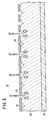
- gaps are formed between the emitter and the surfaces of the peripheral portions of the through regions which face the emitter, and a cluster of capacitors formed from the gaps is formed.
- the capacitance of the cluster of capacitors of the gaps is relatively small. Because of voltage division between the cluster of capacitors and the capacitor of the emitter, almost the entire applied voltage is applied across the gaps, which are effective for each gap to produce a higher output of the electron emission.
- the cluster of capacitors is connected in series to the capacitor of the emitter. Therefore, the overall capacitance is smaller than the capacitance of the capacitor of the emitter. This is effective to provide such preferred characteristics that the electron emission is performed for a higher output and the overall power consumption is lower.
- the amplifying circuit can have an output dynamic range that is about 1000 times as large as an input dynamic range thereof, have a memory function, and can respond to an input signal at a high speed.
- analog data such as sensor output data is converted into digital data and stored in a memory having bits depending on desired accuracy.
- the stored digital data is read from the memory and converted back into analog data, which is output to a drive circuit, for example.
- the memory device according to the present invention does not need expensive A/D and D/A converters, and is free of data accuracy reductions which would be caused by A/D and D/A converting processes.
- a current control unit has an electron emitter that has a memory for accumulating electric charges corresponding to an input voltage, for emitting electrons corresponding to the electric charges accumulated in the memory; and an amplifier connected to a power supply and including a collector electrode for capturing the electrons emitted from the electron emitter, in which a direction and an amount of an output current is controlled based on a direction and an amount of a collector current that flows into the collector electrode when the electrons are emitted from the electron emitter.
- the current control unit has a high withstand voltage and is capable of controlling a current in a wide range of temperature and humidity.
- the piezoelectric/electrostrictive layer may be dense or porous. If the piezoelectric/electrostrictive layer is porous, it may preferably have a porosity of 40 % or less.
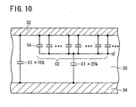
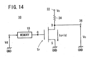
- An equivalent circuit representative of an operation of the microdevice 10 during the emission of electrons from the electron emitter 14 comprises, as shown in FIG. 14, a field effect transistor Tr having a drain D provided by the collector electrode 20, a gate G by the memory 18, and a source S by the GND.
- a voltage drop is developed across the load 24 and extracted as an output voltage (amplified voltage) Vo from the output terminal 36.
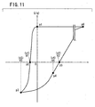
- Output characteristics (drive voltage Vd vs. collector current Ic characteristics) of the microdevice 10 will be described below with reference to FIG. 15.
- the output characteristics are characteristics obtained when a film thickness of the emitter 30 of the electronic emitter 14 is 20 ⁇ m.
- the output characteristics shown in FIG. 15 that as an absolute value of the input voltage Vi is larger, the value of the collector current Ic is larger under the same drive voltage Vd (ex., 200 V), and the collector current Ic is not saturated when the drive voltage Vd is in the range from 0 to about 300 V, and is saturated when the drive voltage Vd is in excess of 300 V.
- the output characteristics of the microdevice 10 are highly similar to those of a transistor.
- an output dynamic range of the microdevice 10 can be controlled by controlling the level of the drive voltage Vd.
- a number of analog switches 130 may be arrayed two-dimensionally for use as an analog multiplexer.
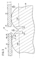
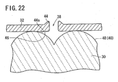
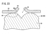
- the upper electrode 32 of the electron emitter 14 has the overhanging portion 44 on the peripheral portion of the through region 38, together with the increased electric field concentration in the region of the gap 46, electrons are easily emitted from the overhanging portion 44 of the upper electrode 32. This leads to a higher output and higher efficiency of the electron emission, making the drive voltage Vd lower.
- the overhanging portion 44 of the upper electrode 32 functions as a gate electrode (a control electrode, a focusing electronic lens, or the like), straightness of emitted electrons can be improved. This is effective in reducing crosstalk between memory devices 110 if a number of memory devices 110 (see FIG.
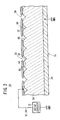
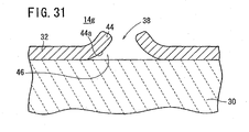
- FIG. 29 shows an electron emitter 14e according to a fifth modification.
- the electron emitter 14e has floating electrodes 160 which are present on a portion of the upper surface of the emitter 30 which corresponds to the through region 38.
- the ceramics of the thinned portion 168 may be stabilized zirconium oxide, aluminum oxide, magnesium oxide, titanium oxide, spinel, mullite, aluminum nitride, silicon nitride, glass, or a mixture thereof.
- aluminum oxide and stabilized zirconium oxide are particularly preferable since they provide high mechanical strength and high rigidity.
- Stabilized zirconium oxide is particularly suitable since it has relatively high mechanical strength, relatively high tenacity, and causes a relatively small chemical reaction with the upper electrode 32 and the lower electrode 34.
- Stabilized zirconium oxide includes both stabilized zirconium oxide and partially stabilized zirconium oxide. Stabilized zirconium oxide does not cause a phase transition since it has a crystalline structure such as a cubic structure or the like.
Landscapes
- Engineering & Computer Science (AREA)
- Physics & Mathematics (AREA)
- Computer Hardware Design (AREA)
- Theoretical Computer Science (AREA)
- Chemical & Material Sciences (AREA)
- Nanotechnology (AREA)
- General Physics & Mathematics (AREA)
- Mathematical Physics (AREA)
- Crystallography & Structural Chemistry (AREA)
- Cold Cathode And The Manufacture (AREA)
- Cathode-Ray Tubes And Fluorescent Screens For Display (AREA)
Applications Claiming Priority (6)
| Application Number | Priority Date | Filing Date | Title |
|---|---|---|---|
| JP2003345992 | 2003-10-03 | ||
| JP2003345992 | 2003-10-03 | ||
| US730754 | 2003-12-08 | ||
| US10/730,754 US7176609B2 (en) | 2003-10-03 | 2003-12-08 | High emission low voltage electron emitter |
| JP2004248101 | 2004-08-27 | ||
| JP2004248101A JP4344664B2 (ja) | 2003-10-03 | 2004-08-27 | マイクロデバイス、マイクロデバイスアレー、増幅回路、メモリ装置、アナログスイッチ及び電流制御素子 |
Publications (1)
| Publication Number | Publication Date |
|---|---|
| EP1521230A2 true EP1521230A2 (fr) | 2005-04-06 |
Family
ID=34317256
Family Applications (1)
| Application Number | Title | Priority Date | Filing Date |
|---|---|---|---|
| EP20040256008 Withdrawn EP1521230A2 (fr) | 2003-10-03 | 2004-09-29 | Dispositif d'affichage à émetteur d'électrons, comprenant une micro matrice, un circuit d'amplification, un dispositif à mémoire, un contacteur analogique et une unité de commande en courant. |
Country Status (2)
| Country | Link |
|---|---|
| EP (1) | EP1521230A2 (fr) |
| JP (1) | JP4344664B2 (fr) |
Cited By (1)
| Publication number | Priority date | Publication date | Assignee | Title |
|---|---|---|---|---|
| EP1768153A4 (fr) * | 2004-06-08 | 2008-11-26 | Ngk Insulators Ltd | Élément d'émission d'électrons et procédé pour la fabrication d'éléments d'émission d'électrons |
Families Citing this family (1)
| Publication number | Priority date | Publication date | Assignee | Title |
|---|---|---|---|---|
| JP5073370B2 (ja) * | 2007-02-19 | 2012-11-14 | 日本碍子株式会社 | 誘電体デバイス及びその製造方法 |
-
2004
- 2004-08-27 JP JP2004248101A patent/JP4344664B2/ja not_active Expired - Fee Related
- 2004-09-29 EP EP20040256008 patent/EP1521230A2/fr not_active Withdrawn
Cited By (1)
| Publication number | Priority date | Publication date | Assignee | Title |
|---|---|---|---|---|
| EP1768153A4 (fr) * | 2004-06-08 | 2008-11-26 | Ngk Insulators Ltd | Élément d'émission d'électrons et procédé pour la fabrication d'éléments d'émission d'électrons |
Also Published As
| Publication number | Publication date |
|---|---|
| JP4344664B2 (ja) | 2009-10-14 |
| JP2005174905A (ja) | 2005-06-30 |
Similar Documents
| Publication | Publication Date | Title |
|---|---|---|
| US7088049B2 (en) | Electron-emitting device and field emission display using the same | |
| US7230371B2 (en) | Light source | |
| US7176609B2 (en) | High emission low voltage electron emitter | |
| US20050073235A1 (en) | Electron emitter, electron emission device, display, and light source | |
| US7719201B2 (en) | Microdevice, microdevice array, amplifying circuit, memory device, analog switch, and current control unit | |
| US7336026B2 (en) | High efficiency dielectric electron emitter | |
| JP3867078B2 (ja) | 電子放出素子 | |
| US7474060B2 (en) | Light source | |
| EP1521230A2 (fr) | Dispositif d'affichage à émetteur d'électrons, comprenant une micro matrice, un circuit d'amplification, un dispositif à mémoire, un contacteur analogique et une unité de commande en courant. | |
| US20040085010A1 (en) | Electron emitter, drive circuit of electron emitter and method of driving electron emitter | |
| US20050073234A1 (en) | Electron emitter | |
| US20060214557A1 (en) | Light source | |
| US6936972B2 (en) | Electron-emitting element and field emission display using the same | |
| US20050116603A1 (en) | Electron emitter | |
| JP3848237B2 (ja) | 電子放出素子及びそれを用いたフィールドエミッションディスプレイ | |
| US20050073232A1 (en) | Electron emitter | |
| US20050280346A1 (en) | Display device | |
| JP4304125B2 (ja) | 電子放出素子 | |
| JP4097230B2 (ja) | 電子放出素子 | |
| US20030038600A1 (en) | Electron-emitting device and field emission display using the same | |
| EP1510998A2 (fr) | Dispositif émetteur d'électrons, source lumineuse et dispositif d'affichage d'images | |
| WO2006075405A1 (fr) | Element d'emission d'electrons | |
| WO2006075407A1 (fr) | Element d'emission d'electrons | |
| WO2006070445A1 (fr) | Source de lumière | |
| WO2006070446A1 (fr) | Element emetteur d’electrons, dispositif emetteur d’electrons, affichage et source de lumiere |
Legal Events
| Date | Code | Title | Description |
|---|---|---|---|
| PUAI | Public reference made under article 153(3) epc to a published international application that has entered the european phase |
Free format text: ORIGINAL CODE: 0009012 |
|
| 17P | Request for examination filed |
Effective date: 20041018 |
|
| AK | Designated contracting states |
Kind code of ref document: A2 Designated state(s): AT BE BG CH CY CZ DE DK EE ES FI FR GB GR HU IE IT LI LU MC NL PL PT RO SE SI SK TR |
|
| AX | Request for extension of the european patent |
Extension state: AL HR LT LV MK |
|
| STAA | Information on the status of an ep patent application or granted ep patent |
Free format text: STATUS: THE APPLICATION HAS BEEN WITHDRAWN |
|
| 18W | Application withdrawn |
Effective date: 20070315 |