EP1523030A2 - Apparat und Methode zur Abtrennung einer Halbleiterscheibe von einem Träger - Google Patents
Apparat und Methode zur Abtrennung einer Halbleiterscheibe von einem Träger Download PDFInfo
- Publication number
- EP1523030A2 EP1523030A2 EP04021396A EP04021396A EP1523030A2 EP 1523030 A2 EP1523030 A2 EP 1523030A2 EP 04021396 A EP04021396 A EP 04021396A EP 04021396 A EP04021396 A EP 04021396A EP 1523030 A2 EP1523030 A2 EP 1523030A2
- Authority
- EP
- European Patent Office
- Prior art keywords
- semiconductor wafer
- adhesive sheet
- faced adhesive
- supporting member
- separating
- Prior art date
- Legal status (The legal status is an assumption and is not a legal conclusion. Google has not performed a legal analysis and makes no representation as to the accuracy of the status listed.)
- Granted
Links
Images
Classifications
-
- H—ELECTRICITY
- H10—SEMICONDUCTOR DEVICES; ELECTRIC SOLID-STATE DEVICES NOT OTHERWISE PROVIDED FOR
- H10W—GENERIC PACKAGES, INTERCONNECTIONS, CONNECTORS OR OTHER CONSTRUCTIONAL DETAILS OF DEVICES COVERED BY CLASS H10
- H10W72/00—Interconnections or connectors in packages
- H10W72/071—Connecting or disconnecting
-
- H—ELECTRICITY
- H10—SEMICONDUCTOR DEVICES; ELECTRIC SOLID-STATE DEVICES NOT OTHERWISE PROVIDED FOR
- H10P—GENERIC PROCESSES OR APPARATUS FOR THE MANUFACTURE OR TREATMENT OF DEVICES COVERED BY CLASS H10
- H10P72/00—Handling or holding of wafers, substrates or devices during manufacture or treatment thereof
- H10P72/04—Apparatus for manufacture or treatment
- H10P72/0442—Apparatus for placing on an insulating substrate, e.g. tape
-
- H—ELECTRICITY
- H10—SEMICONDUCTOR DEVICES; ELECTRIC SOLID-STATE DEVICES NOT OTHERWISE PROVIDED FOR
- H10P—GENERIC PROCESSES OR APPARATUS FOR THE MANUFACTURE OR TREATMENT OF DEVICES COVERED BY CLASS H10
- H10P52/00—Grinding, lapping or polishing of wafers, substrates or parts of devices
Definitions
- the present invention relates to a method of separating a semiconductor wafer held by being joined to a supporting member such as a glass plate via a double-faced adhesive sheet from the supporting member, and to a separating apparatus using the method.
- a semiconductor wafer is subjected to a process of forming a number of devices on the surface of the semiconductor wafer. After that, in a back grind process, the back face of the semiconductor wafer is ground or polished to a desired thickness. The resultant semiconductor wafer is diced into devices in a dicing process.
- means for separating a semiconductor wafer held by being joined to a supporting member via a both-faced adhesive sheet is performed as follows.
- a both-faced adhesive sheet of an ultraviolet curing type whose adhesive strength is weakened by irradiation with an ultraviolet ray is used.
- the adhesive strength is preliminarily decreased.
- the semiconductor wafer is sandwiched by upper and lower two tables and heated in a vacuumed state so as to be shrink-deformed, thereby reducing the contact area between the both-faced adhesive sheet and the semiconductor wafer, and the semiconductor wafer is floated.
- both-faced adhesive sheet used not only a both-faced adhesive sheet of the ultraviolet curing type but also a both-faced adhesive sheet having heating separability which foams when heated and whose adhesive strength decreases are used.
- the conventional means has the following problems.
- the distribution of the adhesive strength largely varies according to conditions such as the degree of shrink deformation of the both-faced adhesive sheet, the degree of ultraviolet curing, and the like.
- the present invention is made in consideration of the above circumstances, and it is a main object thereof to provide a semiconductor wafer separating method and apparatus capable of smoothly separating a semiconductor wafer held by being joined to a supporting member via a both-faced adhesive sheet without stress.
- the present invention employs the following configuration:
- a method for separating a semiconductor wafer joined to a supporting member via a both-faced adhesive sheet from the both-faced adhesive sheet comprising:
- a semiconductor wafer is separated from the both-faced adhesive sheet in a non-contact manner, so that separating stress acting on the semiconductor wafer at the time of separating is small.
- small separating stress acting so as to be dispersed to the periphery of the semiconductor wafer acts toward the center of the semiconductor wafer, so that the semiconductor wafer is separated from the outer end side of the both-faced adhesive sheet toward the center. Therefore, the stress caused by the separating on the semiconductor wafer can be reduced and the semiconductor wafer can be separated smoothly without stress while preventing warp and breakage of the semiconductor wafer.
- the supporting member in the first step, the supporting member is held in a posture that the surface of the supporting member faces downward, and in the second step, the semiconductor wafer is separated from the both-faced adhesive sheet while suspension-holding the semiconductor wafer in a non-contact manner by a differential pressure generated in a gap between the separating means and the back face of the semiconductor wafer by ejecting gas from the separating means toward the back face of the semiconductor wafer.
- the differential pressure from the atmospheric pressure is generated in the gap between the separating means and the back face of a semiconductor wafer by gas ejected toward the back face of the semiconductor wafer, and the semiconductor wafer is suspension-held in the space while maintaining a predetermined distance. Therefore, the semiconductor wafer can be separated in a state where warp stress on the semiconductor wafer generated in the back grinding process is spread and disappears, and transported as it is.
- the supporting member in the first step, the supporting member is held in a posture that the surface of the supporting member faces upward, and in the second step, the semiconductor wafer separated and dropped by dead load from the both-faced adhesive sheet whose adhesive strength is weakened is held.
- a semiconductor wafer is separated and naturally drops by dead load from the both-faced adhesive sheet whose adhesive strength is weakened, and the dropped semiconductor wafer can be properly received and held by transport means.
- the separating stress by the dead load of the semiconductor wafer acts from one end side of the both-faced adhesive sheet, and the semiconductor wafer can be smoothly separated without stress.
- the semiconductor wafer Since the semiconductor wafer is separated from the both-faced adhesive sheet in a posture that the device formation face protected with the both-faced adhesive sheet faces upward, the semiconductor wafer can be mounted as it is onto transport means and transported to the subsequent process. Therefore, a process of turning the separated semiconductor wafer upside down so that the device formation face faces upward becomes unnecessary and it also is advantageous from the viewpoint of improving carry efficiency.
- the supporting member in the first step, the supporting member is held in a posture that the surface of the supporting member faces upward, and in the second step, the semiconductor wafer is separated from the both-faced adhesive sheet whose adhesive strength is weakened while the back side of the semiconductor wafer is sucked.
- a semiconductor wafer is separated and drops by dead load and suction from the both-faced adhesive sheet whose adhesive strength is weakened, and the dropped semiconductor wafer can be properly received and held by the transport means.
- the separating stress by the dead load of the semiconductor wafer and suction acts from one end side of the both-faced adhesive sheet, and the semiconductor wafer can be smoothly separated without stress.
- the semiconductor wafer Since the semiconductor wafer is separated from the both-faced adhesive sheet in a posture that the device formation face protected with the both-faced adhesive sheet faces upward, the semiconductor wafer can be mounted as it is onto transport means and transported to the subsequent process. Therefore, a process of turning the separated semiconductor wafer upside down so that the device formation face faces upward becomes unnecessary and it is also advantageous from the viewpoint of improving carry efficiency.
- the both-faced adhesive sheet any of the following is used.
- a both-faced adhesive sheet whose adhesive strength is weakened by heating or cooling may be used.
- the both-faced adhesive sheet is heated or cooled.
- Another both-faced adhesive sheet is obtained by forming an adhesive layer having heating separability which is foamed and expanded when being heated and loses adhesion strength on at least any of the faces of a sheet base material.
- the both-faced adhesive sheet is heated.
- Still another both-faced adhesive sheet is formed by sandwiching the sheet base material by adhesive layers of an ultraviolet curing type so that the adhesive layers loose their adhesive strengths at different wavelengths.
- the both-faced adhesive sheet is irradiated with an ultraviolet ray.
- the present invention also employs the following configuration:
- An apparatus for separating a semiconductor wafer joined to a supporting member via a both-faced adhesive sheet whose adhesion strength is weakened by heating from the both-faced adhesive sheet comprising:
- the both-faced adhesive sheet is heated by the heating means in a state where the supporting member side is held by the holding means.
- the semiconductor wafer is separated by the separating means in a non-contact manner. Therefore, the semiconductor wafer separating method of the first aspect of the present invention can be suitably realized.
- the separating means separates the semiconductor wafer from the both-faced adhesive sheet while suspension-holding the semiconductor wafer in a non-contact manner by a differential pressure generated in a gap between the separating means and the face of the semiconductor wafer by ejecting gas toward the back face of the semiconductor wafer.
- the holding means holds the surface side of the supporting member, and the separating means is a robot arm for suction-holding the back face of the semiconductor wafer. The robot arm is moved close to the back face of the semiconductor wafer to suck the semiconductor wafer, thereby separating the semiconductor wafer from the both-faced adhesive sheet and suction-holding the semiconductor wafer.
- the present invention also employs the following configuration:
- An apparatus for separating a semiconductor wafer joined to a supporting member via a both-faced adhesive sheet whose adhesion strength is weakened by cooling from the both-faced adhesive sheet comprising:
- the semiconductor wafer separating apparatus in a state where the supporting member side is held by the holding means, the both-faced adhesive sheet is cooled by the cooling means. In a state where the adhesive strength of the cooled both-faced adhesive sheet is weakened, the semiconductor wafer is separated in a non-contact manner by the separating means. Therefore, the separating method of the first aspect of the present invention can be suitably realized.
- the separating means separates the semiconductor wafer from the both-faced adhesive sheet while suspension-holding the semiconductor wafer in a non-contact manner by a differential pressure generated in a gap between the separating means and the back face of the semiconductor wafer by ejecting gas toward the back face of the semiconductor wafer.
- the holding means holds the supporting member in a posture that the surface of the supporting member faces upward
- the separating means is a robot arm for suction-holding the back face of the semiconductor wafer, and the robot arm is moved close to the back face of the semiconductor wafer to suck the semiconductor wafer, thereby separating the semiconductor wafer from the both-faced adhesive sheet and suction-holding the semiconductor wafer.
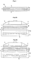
- Fig. 1 shows a work W obtained by joining a supporting member 2 taking the form of a glass plate to a device formation face (surface) of a semiconductor wafer 1 via a both-faced adhesive sheet 3.
- the back face of the semiconductor wafer 1 is backing-reinforced by the supporting member 2
- the back face of the semiconductor wafer 1 is ground to a desired thickness in a back grinding process.
- the semiconductor wafer 1 ground to be thin is separated from the both-faced adhesive sheet 3 and is subjected to the subsequent process.
- the both-faced adhesive sheet 3 is constructed by providing adhesive layers 3b and 3c having heating separability which foam and expand when heated and loose adhesive strength on both sides of a sheet base material 3a.
- the adhesive layers 3b and 3c have different heat separating characteristics in such a manner that the adhesive strength of the adhesive layer 3b for adhesion holding the semiconductor wafer 1 almost disappears at about 70°C and that of the adhesive layer 3c for adhesion holding the supporting member almost disappears at about 120°C.
- the work W is loaded onto a suction chuck stage 4 in a posture that the back face of the semiconductor wafer 1 faces upward and is suction-held on the top face of the suction chuck stage 4 via a suction chuck part 4a from the surface side of the supporting member 2.
- a Bernoulli chuck 5 is disposed above the suction chuck stage 4 so as to be movable in the vertical and horizontal directions via driving means (not shown).
- the Bernoulli chuck 5 ejects gas toward the work W, so that a differential pressure from the atmospheric pressure is generated in a gap between the Bernoulli chuck 5 and the face of the semiconductor wafer 1 by generation of a negative pressure by the ejector effect and the Bernoulli effect and generation of a positive pressure by an air cushion effect, thereby enabling an object positioned below the under face of the Bernoulli chuck 5 to be held in a state where the object floats in the air. Consequently, the Bernoulli chuck 5 is used to suspension-hold or carry an object in a non-contact manner.
- the suction chuck stage 4 has therein a heater 6 and the work W is heated to a temperature at which the adhesive layer 3b on a low temperature side looses its adhesive strength.
- the Bernoulli chuck 5 is lowered to a height with a predetermined small interval to the top face of the work W, that is, the back facing upward of the semiconductor wafer 1 and a non-contact suspending action is exhibited by the gas ejecting operation.
- the small interval is properly changed and determined according to the shape and the weight after grinding of the semiconductor wafer 1 and the suspension holding capability of the Bernoulli chuck 5.
- the small interval is set in a range from 0.1 to 1.0 mm.
- the semiconductor wafer 1 receives suction force of the Bernoulli chuck 5, is separated from the both-faced adhesive sheet 3 and, as shown in Fig. 2B, suspension-held in the non-contact manner with the small interval from the under face of the Bernoulli chuck 5.
- the Bernoulli chuck 5 makes the positive and negative pressures act in order to suspension-hold the semiconductor wafer 1, thereby correcting the warp stress acting on the semiconductor wafer 1 at the time of grinding. That is, the warp stress on the semiconductor wafer 1 can be spread so as to disappear.
- the semiconductor wafer 1 is transported to a desired position.
- the semiconductor wafer 1 can be separated in a non-contact manner in the state where the adhesive strength of the both-faced adhesive sheet 3 joining the supporting member 2 and the semiconductor wafer 1 is almost lost. Since small separating stress acting so as to be dispersed to the periphery of the semiconductor wafer 1 tends to act toward the center of the semiconductor wafer 1, the semiconductor wafer 1 is separated from the outer end side of the both-faced adhesive sheet toward the center. As a result, the stress caused by the separating on the semiconductor wafer 1 can be reduced and the semiconductor wafer 1 can be separated smoothly without stress while preventing warp and breakage of the semiconductor wafer 1.
- the differential pressure from the atmospheric pressure is generated in the gap between the Bernoulli chuck 5 and the face of the semiconductor wafer 1 by generation of a negative pressure due to the ejector effect and the Bernoulli effect and generation of a positive pressure due to the air cushion effect. Consequently, when an object positioned below the under face of the Bernoulli chuck 5 is suspension-held in a state where the object floats in the air, the object can be transported in a state where the warp stress generated when the semiconductor wafer 1 is ground is corrected so as to disappear. As a result, a problem such that when the semiconductor wafer 1 is loaded into a cassette or the like, an end portion of the semiconductor wafer 1 comes into contact with the cassette and is damaged due to a warp or the like can be also avoided.
- the semiconductor wafer 1 since the device formation face of the separated semiconductor wafer 1 faces downward, the semiconductor wafer 1 has to be turned upside down before it is loaded to a processor of the subsequent process. In separating means to be described below, the turning process is unnecessary.
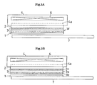
- the work W is loaded below the suction chuck stage 4 in a posture that the back face of the semiconductor wafer 1 faces downward, and is suction-held from the surface side of the supporting member 2 via the suction chuck part 4a by the under face of the suction chuck stage 4.
- a robot arm 7 as a transport arm having suction holes in its top face is disposed below the under face of the work W which is suction-held by the suction chuck stage 4, that is, the back side facing downward of the semiconductor wafer 1 with a predetermined small interval.
- the work W is heated by the heater 6 provided in the suction chuck stage 4.
- the adhesive strength of the adhesive layer 3b almost disappears due to the heating, as shown in Fig. 3B, the semiconductor wafer 1 is separated and dropped from the both-faced adhesive sheet 3 by the dead load and the suction force of the robot arm 7 and received and held by the robot arm 7.
- the semiconductor wafer 1 Since the device formation face of the semiconductor wafer 1 received and suction-held by the robot arm 7 faces upward, by moving the robot arm 7, the semiconductor wafer 1 can be loaded in the posture into the next processor, a housing member, or the like.
- the semiconductor wafer 1 can be separated in a non-contact manner in the state where the adhesion strength of the both-faced adhesive sheet 3 joining the supporting member 3 and the semiconductor wafer 1 is almost disappeared.
- the semiconductor wafer 1 since small separating stress acting so as to be dispersed to the periphery of the semiconductor wafer 1 tends to act toward the center of the semiconductor wafer 1, the semiconductor wafer 1 is separated from the outer end side of the both-faced adhesive sheet toward the center.
- the stress caused by the separating on the semiconductor wafer 1 can be reduced and the semiconductor wafer 1 can be separated smoothly without stress while preventing warp and breakage of the semiconductor wafer 1.
- the surface protection sheet is separated by using a surface protection sheet separating mechanism.
- a separating sheet is joined onto the surface of the adhesive sheet via a separating bar, a separating roller, or the like and, after that, the adhesive sheet integrated with the separating sheet can be separated from the surface of the semiconductor wafer 1.
- the adhesive sheet can be effectively separated from the surface of the semiconductor wafer 1 in a state where unnecessary remaining is almost eliminated.
Landscapes
- Container, Conveyance, Adherence, Positioning, Of Wafer (AREA)
- Mechanical Treatment Of Semiconductor (AREA)
Priority Applications (1)
| Application Number | Priority Date | Filing Date | Title |
|---|---|---|---|
| EP07004502A EP1793415A1 (de) | 2003-10-06 | 2004-09-09 | Apparat und Methode zur Abtrennung einer Halbleiterscheibe von einem Träger |
Applications Claiming Priority (2)
| Application Number | Priority Date | Filing Date | Title |
|---|---|---|---|
| JP2003347059A JP4130167B2 (ja) | 2003-10-06 | 2003-10-06 | 半導体ウエハの剥離方法 |
| JP2003347059 | 2003-10-06 |
Related Child Applications (1)
| Application Number | Title | Priority Date | Filing Date |
|---|---|---|---|
| EP07004502A Division EP1793415A1 (de) | 2003-10-06 | 2004-09-09 | Apparat und Methode zur Abtrennung einer Halbleiterscheibe von einem Träger |
Publications (3)
| Publication Number | Publication Date |
|---|---|
| EP1523030A2 true EP1523030A2 (de) | 2005-04-13 |
| EP1523030A3 EP1523030A3 (de) | 2005-08-31 |
| EP1523030B1 EP1523030B1 (de) | 2007-10-03 |
Family
ID=34309180
Family Applications (2)
| Application Number | Title | Priority Date | Filing Date |
|---|---|---|---|
| EP04021396A Expired - Lifetime EP1523030B1 (de) | 2003-10-06 | 2004-09-09 | Apparat und Methode zur Abtrennung einer Halbleiterscheibe von einem Träger |
| EP07004502A Withdrawn EP1793415A1 (de) | 2003-10-06 | 2004-09-09 | Apparat und Methode zur Abtrennung einer Halbleiterscheibe von einem Träger |
Family Applications After (1)
| Application Number | Title | Priority Date | Filing Date |
|---|---|---|---|
| EP07004502A Withdrawn EP1793415A1 (de) | 2003-10-06 | 2004-09-09 | Apparat und Methode zur Abtrennung einer Halbleiterscheibe von einem Träger |
Country Status (8)
| Country | Link |
|---|---|
| US (1) | US7384811B2 (de) |
| EP (2) | EP1523030B1 (de) |
| JP (1) | JP4130167B2 (de) |
| KR (1) | KR101165094B1 (de) |
| CN (1) | CN100466189C (de) |
| AT (1) | ATE375003T1 (de) |
| DE (1) | DE602004009259T2 (de) |
| TW (1) | TWI286352B (de) |
Cited By (6)
| Publication number | Priority date | Publication date | Assignee | Title |
|---|---|---|---|---|
| WO2010018125A1 (de) * | 2008-08-13 | 2010-02-18 | Ers Electronic Gmbh | Verfahren und vorrichtung zum thermischen bearbeiten von kunststoffscheiben, insbesondere moldwafern |
| WO2011053153A1 (en) * | 2009-10-28 | 2011-05-05 | Dynatec Engineering As | Device for wafer handling |
| WO2015197132A1 (de) * | 2014-06-27 | 2015-12-30 | Erich Thallner | Probenhalter, vorrichtung und verfahren zum lösen eines ersten substrats |
| US20170106644A1 (en) * | 2015-04-03 | 2017-04-20 | Boe Technology Group Co., Ltd. | Disassembly device |
| US20170140971A1 (en) * | 2015-11-14 | 2017-05-18 | Nachiket R. Raravikar | Adhesive with tunable adhesion for handling ultra-thin wafer |
| CN116676586A (zh) * | 2023-06-29 | 2023-09-01 | 中北大学 | 一种碳化硅单晶片的镀膜装置 |
Families Citing this family (32)
| Publication number | Priority date | Publication date | Assignee | Title |
|---|---|---|---|---|
| TWI271815B (en) * | 2004-11-30 | 2007-01-21 | Sanyo Electric Co | Method for processing stuck object and electrostatic sticking method |
| JP4401322B2 (ja) * | 2005-04-18 | 2010-01-20 | 日東電工株式会社 | 支持板分離装置およびこれを用いた支持板分離方法 |
| JP4885483B2 (ja) * | 2005-06-06 | 2012-02-29 | リンテック株式会社 | 転写装置とその方法、剥離装置とその方法、貼付装置とその方法 |
| JP4746003B2 (ja) * | 2007-05-07 | 2011-08-10 | リンテック株式会社 | 移載装置及び移載方法 |
| JP4826593B2 (ja) * | 2008-03-11 | 2011-11-30 | Tdk株式会社 | 電子部品の製造方法 |
| JP4844578B2 (ja) * | 2008-03-11 | 2011-12-28 | Tdk株式会社 | 電子部品の製造方法 |
| JP5203856B2 (ja) * | 2008-08-28 | 2013-06-05 | リンテック株式会社 | シート剥離装置及び剥離方法 |
| US8950459B2 (en) | 2009-04-16 | 2015-02-10 | Suss Microtec Lithography Gmbh | Debonding temporarily bonded semiconductor wafers |
| WO2010121068A2 (en) * | 2009-04-16 | 2010-10-21 | Suss Microtec, Inc. | Improved apparatus for temporary wafer bonding and debonding |
| US9837295B2 (en) | 2010-04-15 | 2017-12-05 | Suss Microtec Lithography Gmbh | Apparatus and method for semiconductor wafer leveling, force balancing and contact sensing |
| US9859141B2 (en) | 2010-04-15 | 2018-01-02 | Suss Microtec Lithography Gmbh | Apparatus and method for aligning and centering wafers |
| JP2012109538A (ja) * | 2010-10-29 | 2012-06-07 | Tokyo Ohka Kogyo Co Ltd | 積層体、およびその積層体の分離方法 |
| JP5802106B2 (ja) | 2010-11-15 | 2015-10-28 | 東京応化工業株式会社 | 積層体、および分離方法 |
| CN102543662B (zh) * | 2010-12-30 | 2016-02-03 | 上海微电子装备有限公司 | 热盘及应用其的硅片加热系统 |
| JP5323867B2 (ja) * | 2011-01-19 | 2013-10-23 | 東京エレクトロン株式会社 | 基板反転装置、基板反転方法、剥離システム、プログラム及びコンピュータ記憶媒体 |
| WO2012140987A1 (ja) * | 2011-04-12 | 2012-10-18 | 東京エレクトロン株式会社 | 剥離装置、剥離システム及び剥離方法 |
| JP5149977B2 (ja) * | 2011-04-15 | 2013-02-20 | リンテック株式会社 | 半導体ウエハの処理方法 |
| JP2013004845A (ja) * | 2011-06-20 | 2013-01-07 | Tokyo Electron Ltd | 剥離システム、剥離方法、プログラム及びコンピュータ記憶媒体 |
| JP5685554B2 (ja) * | 2012-01-17 | 2015-03-18 | 東京エレクトロン株式会社 | 剥離装置、剥離システム、剥離方法および剥離プログラム |
| JP2014044974A (ja) * | 2012-08-24 | 2014-03-13 | Tokyo Electron Ltd | 剥離装置、剥離システム、剥離方法、プログラム及びコンピュータ記憶媒体 |
| HK1216357A1 (en) * | 2012-11-30 | 2016-11-04 | Nikon Corporation | Transfer system, exposure apparatus, transfer method, exposure method, device manufacturing method, and suction apparatus |
| KR102046534B1 (ko) | 2013-01-25 | 2019-11-19 | 삼성전자주식회사 | 기판 가공 방법 |
| US9349645B2 (en) * | 2013-10-16 | 2016-05-24 | Nxp B.V. | Apparatus, device and method for wafer dicing |
| KR102313768B1 (ko) * | 2015-05-06 | 2021-10-18 | 쑤저우 레킨 세미컨덕터 컴퍼니 리미티드 | 양면 테이프 및 이를 이용한 발광소자 제조방법 |
| CN106920759B (zh) * | 2015-12-28 | 2020-04-24 | 上海新微技术研发中心有限公司 | 一种芯片保护壳去除方法及装置 |
| JP6427131B2 (ja) | 2016-03-18 | 2018-11-21 | 株式会社荏原製作所 | 研磨装置および研磨方法 |
| JP7234109B2 (ja) * | 2016-11-15 | 2023-03-07 | コーニング インコーポレイテッド | 基板を加工する方法 |
| CN111095489B (zh) * | 2017-09-12 | 2023-11-28 | 日本碍子株式会社 | 芯片部件的制造方法 |
| KR102505213B1 (ko) * | 2017-12-08 | 2023-03-03 | 삼성전자주식회사 | 분리용 전자 장치 및 이의 공정 방법 |
| CN111403301B (zh) * | 2020-02-07 | 2025-02-25 | Pyxiscf私人有限公司 | 面板自动处理装置和面板自动处理方法 |
| KR102764369B1 (ko) * | 2020-05-15 | 2025-02-07 | 삼성전자주식회사 | 기판 디본딩 장치 |
| DE102020003736A1 (de) | 2020-06-22 | 2021-12-23 | Mycon Gmbh | Vorrichtung und Verfahren zum bauteilschonenden Trennen von Klebverbindungen |
Family Cites Families (29)
| Publication number | Priority date | Publication date | Assignee | Title |
|---|---|---|---|---|
| JPS60216567A (ja) * | 1985-03-11 | 1985-10-30 | Hitachi Ltd | ウエハの切削装置 |
| JPH0369112A (ja) * | 1989-08-08 | 1991-03-25 | Fujitsu Ltd | ホットプレートオーブン |
| US5169196A (en) * | 1991-06-17 | 1992-12-08 | Safabakhsh Ali R | Non-contact pick-up head |
| KR0129119B1 (ko) * | 1992-11-27 | 1998-04-07 | 모리시다 요이찌 | 반도체칩의 제거방법 및 제거장치 |
| KR0144164B1 (ko) * | 1995-05-12 | 1998-07-01 | 문정환 | 엘오씨 반도체 패키지 및 반도체 장치를 패키징하는 방법 |
| ATE261612T1 (de) * | 1996-12-18 | 2004-03-15 | Canon Kk | Vefahren zum herstellen eines halbleiterartikels unter verwendung eines substrates mit einer porösen halbleiterschicht |
| US6017776A (en) * | 1997-04-29 | 2000-01-25 | Micron Technology, Inc. | Method of attaching a leadframe to singulated semiconductor dice |
| KR100278137B1 (ko) * | 1997-09-04 | 2001-01-15 | 가나이 쓰도무 | 반도체소자의 탑재방법 및 그 시스템, 반도체소자 분리장치 및ic카드의 제조방법 |
| JP2000036501A (ja) * | 1998-05-12 | 2000-02-02 | Sharp Corp | ダイボンド装置 |
| JP3816253B2 (ja) * | 1999-01-19 | 2006-08-30 | 富士通株式会社 | 半導体装置の製造方法 |
| JP4275254B2 (ja) * | 1999-06-17 | 2009-06-10 | リンテック株式会社 | 両面粘着シートに固定された物品の剥離方法および剥離装置 |
| JP3597754B2 (ja) * | 2000-04-24 | 2004-12-08 | Necエレクトロニクス株式会社 | 半導体装置及びその製造方法 |
| JP4456234B2 (ja) * | 2000-07-04 | 2010-04-28 | パナソニック株式会社 | バンプ形成方法 |
| US6319754B1 (en) * | 2000-07-10 | 2001-11-20 | Advanced Semiconductor Engineering, Inc. | Wafer-dicing process |
| JP3906962B2 (ja) * | 2000-08-31 | 2007-04-18 | リンテック株式会社 | 半導体装置の製造方法 |
| DE10048881A1 (de) * | 2000-09-29 | 2002-03-07 | Infineon Technologies Ag | Vorrichtung und Verfahren zum planen Verbinden zweier Wafer für ein Dünnschleifen und ein Trennen eines Produkt-Wafers |
| JP3748375B2 (ja) * | 2000-11-24 | 2006-02-22 | シャープ株式会社 | 半導体チップのピックアップ装置 |
| JP2002237515A (ja) * | 2001-02-07 | 2002-08-23 | Mitsubishi Gas Chem Co Inc | 薄葉化半導体基板の剥離装置および剥離法 |
| JP4482243B2 (ja) * | 2001-03-13 | 2010-06-16 | 株式会社新川 | ダイのピックアップ方法及びピックアップ装置 |
| JP3800977B2 (ja) * | 2001-04-11 | 2006-07-26 | 株式会社日立製作所 | Zn−Al系はんだを用いた製品 |
| DE10128923A1 (de) * | 2001-06-15 | 2003-01-23 | Philips Corp Intellectual Pty | Verfahren zum Umsetzen eines im wesentlichen scheibenförmigen Werkstücks und Vorrichtung zur Durchführung dieses Verfahrens |
| JP4266106B2 (ja) * | 2001-09-27 | 2009-05-20 | 株式会社東芝 | 粘着性テープの剥離装置、粘着性テープの剥離方法、半導体チップのピックアップ装置、半導体チップのピックアップ方法及び半導体装置の製造方法 |
| US7332819B2 (en) * | 2002-01-09 | 2008-02-19 | Micron Technology, Inc. | Stacked die in die BGA package |
| DE10212420A1 (de) * | 2002-03-21 | 2003-10-16 | Erich Thallner | Einrichtung zur Aufnahme eines Wafers |
| US6861321B2 (en) * | 2002-04-05 | 2005-03-01 | Asm America, Inc. | Method of loading a wafer onto a wafer holder to reduce thermal shock |
| JP3831287B2 (ja) * | 2002-04-08 | 2006-10-11 | 株式会社日立製作所 | 半導体装置の製造方法 |
| JP3704113B2 (ja) * | 2002-09-26 | 2005-10-05 | 住友大阪セメント株式会社 | ボンディングステージ及び電子部品実装装置 |
| KR100480628B1 (ko) * | 2002-11-11 | 2005-03-31 | 삼성전자주식회사 | 에어 블로잉을 이용한 칩 픽업 방법 및 장치 |
| US20050056946A1 (en) * | 2003-09-16 | 2005-03-17 | Cookson Electronics, Inc. | Electrical circuit assembly with improved shock resistance |
-
2003
- 2003-10-06 JP JP2003347059A patent/JP4130167B2/ja not_active Expired - Fee Related
-
2004
- 2004-09-09 EP EP04021396A patent/EP1523030B1/de not_active Expired - Lifetime
- 2004-09-09 EP EP07004502A patent/EP1793415A1/de not_active Withdrawn
- 2004-09-09 DE DE602004009259T patent/DE602004009259T2/de not_active Expired - Fee Related
- 2004-09-09 AT AT04021396T patent/ATE375003T1/de not_active IP Right Cessation
- 2004-09-13 US US10/938,645 patent/US7384811B2/en not_active Expired - Fee Related
- 2004-09-20 TW TW093128372A patent/TWI286352B/zh not_active IP Right Cessation
- 2004-09-30 CN CNB2004100834438A patent/CN100466189C/zh not_active Expired - Fee Related
- 2004-10-01 KR KR1020040078197A patent/KR101165094B1/ko not_active Expired - Fee Related
Cited By (12)
| Publication number | Priority date | Publication date | Assignee | Title |
|---|---|---|---|---|
| WO2010018125A1 (de) * | 2008-08-13 | 2010-02-18 | Ers Electronic Gmbh | Verfahren und vorrichtung zum thermischen bearbeiten von kunststoffscheiben, insbesondere moldwafern |
| US9177845B2 (en) | 2008-08-13 | 2015-11-03 | Ers Electronic Gmbh | Method and apparatus for thermally processing plastic discs, in particular mould wafers |
| WO2011053153A1 (en) * | 2009-10-28 | 2011-05-05 | Dynatec Engineering As | Device for wafer handling |
| WO2015197132A1 (de) * | 2014-06-27 | 2015-12-30 | Erich Thallner | Probenhalter, vorrichtung und verfahren zum lösen eines ersten substrats |
| CN106716615A (zh) * | 2014-06-27 | 2017-05-24 | 埃里希·塔尔纳 | 用于分离第一衬底的试样固持器,装置和方法 |
| US10276409B2 (en) | 2014-06-27 | 2019-04-30 | Erich Thallner | Sample holder, device and method for detaching of a first substrate |
| CN106716615B (zh) * | 2014-06-27 | 2020-07-10 | 埃里希·塔尔纳 | 用于分离第一衬底的试样固持器,装置和方法 |
| US20170106644A1 (en) * | 2015-04-03 | 2017-04-20 | Boe Technology Group Co., Ltd. | Disassembly device |
| US9937700B2 (en) * | 2015-04-03 | 2018-04-10 | Boe Technology Group Co., Ltd. | Disassembly device |
| US20170140971A1 (en) * | 2015-11-14 | 2017-05-18 | Nachiket R. Raravikar | Adhesive with tunable adhesion for handling ultra-thin wafer |
| WO2020032911A3 (en) * | 2015-11-14 | 2020-07-09 | Intel Corporation | Adhesive with tunable adhesion for handling ultra-thin wafer |
| CN116676586A (zh) * | 2023-06-29 | 2023-09-01 | 中北大学 | 一种碳化硅单晶片的镀膜装置 |
Also Published As
| Publication number | Publication date |
|---|---|
| KR20050033440A (ko) | 2005-04-12 |
| TWI286352B (en) | 2007-09-01 |
| TW200520083A (en) | 2005-06-16 |
| JP2005116678A (ja) | 2005-04-28 |
| EP1793415A1 (de) | 2007-06-06 |
| DE602004009259D1 (de) | 2007-11-15 |
| CN100466189C (zh) | 2009-03-04 |
| US20050074952A1 (en) | 2005-04-07 |
| DE602004009259T2 (de) | 2008-07-10 |
| US7384811B2 (en) | 2008-06-10 |
| ATE375003T1 (de) | 2007-10-15 |
| EP1523030A3 (de) | 2005-08-31 |
| KR101165094B1 (ko) | 2012-07-12 |
| EP1523030B1 (de) | 2007-10-03 |
| CN1606134A (zh) | 2005-04-13 |
| JP4130167B2 (ja) | 2008-08-06 |
Similar Documents
| Publication | Publication Date | Title |
|---|---|---|
| US7384811B2 (en) | Method of separating semiconductor wafer, and separating apparatus using the same | |
| US7393757B2 (en) | Method for separating semiconductor wafer from supporting member, and apparatus using the same | |
| US6418999B1 (en) | Sample separating apparatus and method, and substrate manufacturing method | |
| US8182649B2 (en) | Fixed jig, chip pickup method and chip pickup apparatus | |
| KR101429283B1 (ko) | 기판 접합 방법 및 이를 이용한 장치 | |
| JP2012119431A (ja) | 半導体ウエハ搬送方法および半導体ウエハ搬送装置 | |
| JP6188123B2 (ja) | 貼合装置および貼合処理方法 | |
| JP2000208447A (ja) | 半導体製造装置及び半導体装置の製造方法 | |
| TW201338076A (zh) | 基板搬送方法及基板搬送裝置 | |
| KR20100127713A (ko) | 웨이퍼 마운트 방법과 웨이퍼 마운트 장치 | |
| KR20110106814A (ko) | 점착 테이프 부착 방법 및 점착 테이프 부착 장치 | |
| EP2624292B1 (de) | Substrattransportverfahren und Substrattransportvorrichtung | |
| JP2006191144A (ja) | ピックアップ装置及びピックアップ方法 | |
| US20030013273A1 (en) | Method of manufacturing SOI wafer | |
| JP4677717B2 (ja) | Soiウェーハの製造方法およびその装置 | |
| JP2858567B2 (ja) | 半導体ウエハ用保護シート及び半導体ウエハの保管輸送方法 | |
| JP5373008B2 (ja) | 基板貼合せ方法 | |
| JP6622254B2 (ja) | 貼合装置および貼合処理方法 | |
| JP2003197710A (ja) | 板状物の薄層加工装置及び板状物の薄層加工方法 | |
| JPH1187283A (ja) | 半導体製造装置における平面研削装置 |
Legal Events
| Date | Code | Title | Description |
|---|---|---|---|
| PUAI | Public reference made under article 153(3) epc to a published international application that has entered the european phase |
Free format text: ORIGINAL CODE: 0009012 |
|
| AK | Designated contracting states |
Kind code of ref document: A2 Designated state(s): AT BE BG CH CY CZ DE DK EE ES FI FR GB GR HU IE IT LI LU MC NL PL PT RO SE SI SK TR |
|
| AX | Request for extension of the european patent |
Extension state: AL HR LT LV MK |
|
| PUAL | Search report despatched |
Free format text: ORIGINAL CODE: 0009013 |
|
| AK | Designated contracting states |
Kind code of ref document: A3 Designated state(s): AT BE BG CH CY CZ DE DK EE ES FI FR GB GR HU IE IT LI LU MC NL PL PT RO SE SI SK TR |
|
| AX | Request for extension of the european patent |
Extension state: AL HR LT LV MK |
|
| 17P | Request for examination filed |
Effective date: 20051006 |
|
| AKX | Designation fees paid |
Designated state(s): AT BE DE |
|
| 17Q | First examination report despatched |
Effective date: 20060829 |
|
| GRAP | Despatch of communication of intention to grant a patent |
Free format text: ORIGINAL CODE: EPIDOSNIGR1 |
|
| GRAS | Grant fee paid |
Free format text: ORIGINAL CODE: EPIDOSNIGR3 |
|
| GRAA | (expected) grant |
Free format text: ORIGINAL CODE: 0009210 |
|
| AK | Designated contracting states |
Kind code of ref document: B1 Designated state(s): AT BE DE |
|
| REF | Corresponds to: |
Ref document number: 602004009259 Country of ref document: DE Date of ref document: 20071115 Kind code of ref document: P |
|
| PLBE | No opposition filed within time limit |
Free format text: ORIGINAL CODE: 0009261 |
|
| STAA | Information on the status of an ep patent application or granted ep patent |
Free format text: STATUS: NO OPPOSITION FILED WITHIN TIME LIMIT |
|
| 26N | No opposition filed |
Effective date: 20080704 |
|
| BERE | Be: lapsed |
Owner name: NITTO DENKO CORP. Effective date: 20080930 |
|
| PG25 | Lapsed in a contracting state [announced via postgrant information from national office to epo] |
Ref country code: BE Free format text: LAPSE BECAUSE OF NON-PAYMENT OF DUE FEES Effective date: 20080930 |
|
| PG25 | Lapsed in a contracting state [announced via postgrant information from national office to epo] |
Ref country code: DE Free format text: LAPSE BECAUSE OF NON-PAYMENT OF DUE FEES Effective date: 20090401 |
|
| PG25 | Lapsed in a contracting state [announced via postgrant information from national office to epo] |
Ref country code: AT Free format text: LAPSE BECAUSE OF NON-PAYMENT OF DUE FEES Effective date: 20080909 |