EP1523047B1 - Nitrid-basierte lichtemittierende Halbleitervorrichtung und Herstellungsverfahren dafür - Google Patents
Nitrid-basierte lichtemittierende Halbleitervorrichtung und Herstellungsverfahren dafür Download PDFInfo
- Publication number
- EP1523047B1 EP1523047B1 EP04256154A EP04256154A EP1523047B1 EP 1523047 B1 EP1523047 B1 EP 1523047B1 EP 04256154 A EP04256154 A EP 04256154A EP 04256154 A EP04256154 A EP 04256154A EP 1523047 B1 EP1523047 B1 EP 1523047B1
- Authority
- EP
- European Patent Office
- Prior art keywords
- layer
- light emitting
- emitting device
- contact layer
- group
- Prior art date
- Legal status (The legal status is an assumption and is not a legal conclusion. Google has not performed a legal analysis and makes no representation as to the accuracy of the status listed.)
- Expired - Lifetime
Links
Images




Classifications
-
- H—ELECTRICITY
- H10—SEMICONDUCTOR DEVICES; ELECTRIC SOLID-STATE DEVICES NOT OTHERWISE PROVIDED FOR
- H10H—INORGANIC LIGHT-EMITTING SEMICONDUCTOR DEVICES HAVING POTENTIAL BARRIERS
- H10H20/00—Individual inorganic light-emitting semiconductor devices having potential barriers, e.g. light-emitting diodes [LED]
- H10H20/80—Constructional details
- H10H20/83—Electrodes
- H10H20/832—Electrodes characterised by their material
- H10H20/833—Transparent materials
-
- H—ELECTRICITY
- H10—SEMICONDUCTOR DEVICES; ELECTRIC SOLID-STATE DEVICES NOT OTHERWISE PROVIDED FOR
- H10H—INORGANIC LIGHT-EMITTING SEMICONDUCTOR DEVICES HAVING POTENTIAL BARRIERS
- H10H20/00—Individual inorganic light-emitting semiconductor devices having potential barriers, e.g. light-emitting diodes [LED]
- H10H20/01—Manufacture or treatment
- H10H20/032—Manufacture or treatment of electrodes
-
- H—ELECTRICITY
- H10—SEMICONDUCTOR DEVICES; ELECTRIC SOLID-STATE DEVICES NOT OTHERWISE PROVIDED FOR
- H10H—INORGANIC LIGHT-EMITTING SEMICONDUCTOR DEVICES HAVING POTENTIAL BARRIERS
- H10H20/00—Individual inorganic light-emitting semiconductor devices having potential barriers, e.g. light-emitting diodes [LED]
- H10H20/80—Constructional details
- H10H20/81—Bodies
- H10H20/822—Materials of the light-emitting regions
- H10H20/824—Materials of the light-emitting regions comprising only Group III-V materials, e.g. GaP
- H10H20/825—Materials of the light-emitting regions comprising only Group III-V materials, e.g. GaP containing nitrogen, e.g. GaN
-
- H—ELECTRICITY
- H10—SEMICONDUCTOR DEVICES; ELECTRIC SOLID-STATE DEVICES NOT OTHERWISE PROVIDED FOR
- H10H—INORGANIC LIGHT-EMITTING SEMICONDUCTOR DEVICES HAVING POTENTIAL BARRIERS
- H10H20/00—Individual inorganic light-emitting semiconductor devices having potential barriers, e.g. light-emitting diodes [LED]
- H10H20/80—Constructional details
- H10H20/83—Electrodes
- H10H20/832—Electrodes characterised by their material
- H10H20/835—Reflective materials
Definitions
- the present invention relates to a nitride-based light emitting device and a method of manufacturing the same, and more particularly, to a nitride-based light emitting device with a transparent film electrode structure designed to provide a low specific contact resistance and high light transmittance and a method of manufacturing the same.
- LEDs light emitting diodes
- LDs laser diodes
- GaN gallium nitride
- GaN-based light emitting devices are classified into top-emitting LEDs (TLEDs) and flip-chip LEDs (FCLEDs).
- TLEDs top-emitting LEDs
- FCLEDs flip-chip LEDs
- TLEDs employing a Ni/Au ohmic contact layer, light exits through the ohmic contact layer in contact with a p-cladding layer.
- a Ni/Au layer acts as a semi-transparent ohmic contact layer having an excellent specific contact resistance of 10 -4 to 10 -3 ⁇ cm 2 .
- Annealing of the Ni/Au layer at a temperature of 500 to 600°C in an oxygen (O 2 ) atmosphere leads to the formation of nickel oxide (NiO) at the interface between the p-GaN cladding layer and the Ni layer, thereby lowering a Schottky barrier height (SBH).
- SiO nickel oxide
- SBH Schottky barrier height
- Annealing of Ni/Au on the p-cladding layer results in dissociation of a Mg-H complex in the GaN, which reactivates Mg dopants by increasing the concentration of Mg dopants on the surface of the GaN.
- the effective carrier concentration increases above 10 19 holes/cm 3 on the surface of the p-cladding layer, which causes tunneling conductance between the p-cladding layer and the ohmic contact layer containing NiO, thus obtaining an improved ohmic conductance.
- ITO indium tin oxide
- a transparent conductive oxide having superior light transmittance over a semi-transparent Ni/Au used as the conventional p-ohmic contact layer.
- an ITO ohmic contact layer requires a high operating voltage due to a high ohmic contact resistance between p-GaN and 10 ITO, which generates much heat.
- JP 2002-164570 A discloses that high output power was obtained using p-ZnO as a transparent electrode layer.
- US 5,889,295 describes a GaN-based semiconductor light emitting device with a ZnO layer.
- Al is used to n-type dope the ZnO layer contacting p-GaN.
- Ni/ZnO Al films were deposited on the GaN by an electron beam evaporation and a sputtering system, respectively.
- a nitride-based light emitting device according to claim 1.
- the present invention provides a nitride-based light emitting device same according to claim 1 with a transparent film electrode structure designed to provide a low specific contact resistance and high light transmittance, and a method of manufacturing the according to claim 10.
- the p-type dopant may be at least one of phosphorus (P) and nitrogen (N).
- concentration of the p-type dopant contained in the Zn-containing oxide may be in the range of 0.01 to 30 percent by weight.
- the contact layer may be formed to a thickness of 0.1 to 1,000 nm.
- the light emitting device may further comprise a reflective layer composed of at least one element selected from the group consisting of Ag, Al, Zn, Mg, Ru, Ti, Rh, Cr, and Pt formed on the contact layer.
- the reflective layer may be formed to a thickness of 10 to 2,000 nm.
- the light emitting device may further comprise a first electrode layer composed of at least one element selected from the group consisting of Ni, Au, Pt, Pd, Mg, Cu, Zn, Ag, Sc, Co, Rh, Li, Be, Ca, Ru, Re, Ti, Ta, Na, and La interposed between the p-cladding layer and the contact layer.
- a first electrode layer composed of at least one element selected from the group consisting of Ni, Au, Pt, Pd, Mg, Cu, Zn, Ag, Sc, Co, Rh, Li, Be, Ca, Ru, Re, Ti, Ta, Na, and La interposed between the p-cladding layer and the contact layer.
- the light emitting device may further comprise a second electrode layer composed of at least one element selected from the group consisting of Ni, Au, Pt, Pd, Mg, Cu, Zn, Ag, Sc, Co, Rh, Li, Be, Ca, Ru, Re, Ti, Ta, Na, and La interposed between the contact layer and the reflective layer.
- a second electrode layer composed of at least one element selected from the group consisting of Ni, Au, Pt, Pd, Mg, Cu, Zn, Ag, Sc, Co, Rh, Li, Be, Ca, Ru, Re, Ti, Ta, Na, and La interposed between the contact layer and the reflective layer.
- the active layer may have an InGaN/GaN multiquantum well (MQW) or AlGaN/GaN MQW structure.
- MQW InGaN/GaN multiquantum well
- AlGaN/GaN MQW structure AlGaN/GaN MQW structure.
- the method may further comprise forming an n-current blocking layer on the p-cladding layer before forming the contact layer.
- the n-current blocking layer may be formed to a thickness of 0.1 to 500 nm.
- the n-current blocking layer may be composed of a transparent conductive oxide or an n-GaN-based compound.
- the transparent conductive oxide may be one selected from the group consisting of In 2 O 3 , SnO 2 , and indium tin oxide (ITO).
- the method may further comprise, before forming the contact layer, forming a first electrode layer on the p-cladding layer from at least one element selected from the group consisting of Ni, Au, Pt, Pd, Mg, Cu, Zn, Ag, Sc, Co, Rh, Li, Be, Ca, Ru, Re, Ti, Ta, Na, and La.
- the method may further comprise, before the annealing, forming a second electrode layer on the contact layer from at least one element selected from the group consisting of Ni, Au, Pt, Pd, Mg, Cu, Zn, Ag, Sc, Co, Rh, Li, Be, Ca, Ru, Re, Ti, Ta, Na, and La.
- the method may further comprise, before the annealing, forming a reflective layer on the contact layer from at least one element selected from the group consisting of Ag, Al, Zn, Mg, Ru, Ti, Rh, Cr, and Pt.
- the method may further comprise, before the annealing, forming a second electrode layer between the reflective layer and the contact layer from at least one element selected from the group consisting of Ni, Au, Pt, Pd, Mg, Cu, Zn, Ag, Sc, Co, Rh, Li, Be, Ca, Ru, Re, Ti, Ta, Na, and La.
- the reflective layer may be formed to a thickness of 10 to 2,000 nm.
- the first electrode layer may be formed to a thickness of 0.1 to 1,000 nm.
- the annealing may be performed at a temperature of 100 to 800°C for 10 seconds to 3 hours.
- the annealing may be performed in a gaseous atmosphere containing at least one of N 2 , Ar, He, O 2 , H, and air.
- a p-electrode structure according to a first embodiment of the present invention includes a contact layer 30, which acts as a transparent film electrode.
- a III-nitride-based p-cladding layer 20 and the contact layer 30 are sequentially formed on a substrate 10.
- the p-cladding layer 20 contains a p-type dopant in a III-nitride-based compound represented by the general formula Al x ln y Ga z N (0 ⁇ x ⁇ 1, 0 ⁇ y ⁇ 1, 0 ⁇ z ⁇ 1, 0 ⁇ x+y+z ⁇ 1).
- the p-type dopant may be Mg, Zn, Ca, Sr, or Ba.
- the contact layer 30 contains at least one of P and N in a Zn-containing oxide.
- the Zn-containing oxide is a ternary compound selected from M gx Zn 1-x O, or Be x Zn 1-x O. That is, the contact layer 30 is p-Mg x Zn 1-x O, or p-Be x Zn 1-x O by adding at least one of P and N as the p-type dopant to Mg x Zn 1-x O or Be x Zn 1-x O, respectively.
- the concentration of the p-type dopant contained in the Zn-containing oxide is in the range of 0.01 to 30 percent by weight (weight %).
- a solid compound such as Zn 3 P 2 , ZnP 2 , Mg 3 P 2 , Zn 3 N 2 , or Mg 3 N 2 may be used as the p-type dopant instead of a conventionally used solid oxide such as P 2 O 5 .
- the above-identified solid compounds allow for easier adjustment of carrier or hole concentration in the p-cladding layer 20 and the contact layer 30 than a solid oxide, it is easy to form the contact layer 30 having excellent ohmic contact characteristics.
- ternary p-type Zn-containing oxides containing Mg or Be as the p-type dopant in the p-cladding layer 20 can increase the effective hole concentration in the p-type cladding layer 20, thereby improving the ohmic contact characteristics of the contact layer 30.
- the ternary p-type Zn-containing oxide can also have a larger bandgap than the binary p-type Zn-containing oxide (p-ZnO) , thereby improving the light emission efficiency when used in the contact layer 30 in an AlGaN/GaN light emitting device.
- the thickness of the contact layer 30 ranges from 0.1 to 1,000 nm.
- the contact layer 30 may be deposited using an electron-beam (e-beam) evaporator, a thermal evaporator, sputtering deposition, or pulsed laser deposition (PLD).
- e-beam electron-beam
- PLD pulsed laser deposition
- the deposition temperature ranges from 20 to 1,500°C and the pressure within an evaporator ranges from about 1,33 ⁇ 10 -10 Pa (10 -12 Torr) to atmospheric pressure.
- FIG. 2 is a cross-sectional view of a p-electrode structure according to a second embodiment of the present invention.
- the p-electrode structure includes a contact layer 30 and a reflective layer 40.
- An III-nitride-based p-cladding layer 20, the contact layer 30, and the reflective layer 40 are sequentially formed on a substrate 10.
- the contact layer 30 has the same composition and characteristics as that in the first embodiment.
- the reflective layer 40 which is the uppermost layer in the p-electrode structure, is used for fabrication of a flip-chip light emitting diode and is composed of a material that exhibits oxidation stability, consistent characteristics, and high reflectivity and can prevent surface degradation at temperature of 200 to 600°C.
- the reflective layer 40 may be made of a reflective element selected from the group consisting of Ag, Al, Zn, Mg, Ru, Ti, Rh, Cr, and Pt.
- the thickness of the reflective layer 40 may be in the range of about 10 to about 2,000 nm.
- the reflective layer 40 may be formed using an e-beam evaporator.
- the contact layer 30 and the reflective layer 40 are annealed after deposition to form an ohmic contact between the contact layer 30 and the p-cladding layer 20.
- Annealing is performed at a temperature of 100 to 800°C in vacuum or in a gaseous atmosphere for 10 seconds to 3 hours.
- At least one of N 2 , Ar, He, O 2 , H 2 , and air may be injected into a reactor during annealing.
- a photoresist is spin coated on the p-cladding layer 20 at 4,500 rpm, followed by soft baking of the p-cladding layer 20 for 15 minutes at 85°C. Subsequently, to develop a mask pattern, a mask is aligned relative to the specimen and 22.8 mW ultraviolet (UV) light is then irradiated on the mask for 15 seconds. The resultant structure is then developed for 25 seconds within a developer diluted at a ratio of 1:4 with distilled water, and then immersed in a BOE solution for 5 minutes, which allows a contamination layer to be removed from the developed specimen.
- UV ultraviolet
- ZnO in a powder form is mixed with Zn 3 P 2 in the ratio of about 9.5:0.5 and sintered to produce a sample that is then mounted onto a stage within a chamber of the e-beam evaporator.
- Lift-off is performed by immersing the specimen in acetone and then the specimen is annealed for 1 minute in a rapid thermal annealer (RTA) in an air and N 2 atmosphere ambient at 530°C to form the p-electrode structure.
- RTA rapid thermal annealer
- FIG. 3 is a graph showing electrical characteristics of the structures, nof forming part of the present invention, obtained before and after annealing in the air and N 2 atmosphere at 530°C after depositing the contact layer 30 composed of p-ZnO doped with P on the p-GaN cladding layer 20 with a carrier concentration of 4 ⁇ 10 17 cm -3 to 5 ⁇ 10 17 cm 13 such that the combination of the contact layer 30 and the p-GaN cladding layer 20 has a thickness of about 300 nm.
- the non-annealed p-GaN/p-ZnO structure exhibits nonlinear I-V characteristics indicating a rectifying characteristic while the annealed structure has linear I-V characteristics indicating an ohmic contact characteristic, and has a low specific contact resistance of about 10 -5 to 10 -4 ⁇ cm 2 .
- FIG. 4 is a graph showing electrical characteristics of the structures, not forming part of the present invention, obtained before and after annealing in the air and N 2 atmosphere at 530°C after sequentially depositing the contact layer 30 made of p-ZnO doped with P to a thickness of about 100 nm and Ag reflective layer 40 to a thickness of about 200 nm on the p-GaN cladding layer 20 with a carrier concentration of 4 ⁇ 10 17 cm -3 to 5 ⁇ 10 17 cm -3 .
- the non-annealed p-GaN/ p-ZnO/Ag structure exhibits nonlinear I-V characteristics indicating a rectifying characteristic while the annealed structure has linear I-V characteristics indicating an ohmic contact characteristic, and has a low specific contact resistance of about 10 -5 to 10 -4 ⁇ cm 2 .
- the electrode structure including the contact layer 30 and the reflective layer 40 exhibits superior I-V characteristics over the electrode structure not including the reflective layer 40.
- FIG. 5 shows an example of a light emitting device according to the present invention, incorporating the p-electrode structure shown in FIG. 1 .
- the light emitting device includes a substrate 110, and a buffer layer 120, an n-cladding layer 130, an active layer 140, a p-cladding layer 150 and a contact layer 230 sequentially formed on the substrate 110.
- the light emitting device further includes a p-electrode pad 180 and an n-electrode pad 190.
- the substrate 110 may be formed of sapphire or silicon carbide (SiC).
- the buffer layer 120 does not need to be included.
- Each of the buffer layer 120 the n-cladding layer 130, the active layer 140 and the p-cladding layer 150 is essentially composed of III-nitride-based compound represented by the general formula Al x ln y Ga z N (0 ⁇ x ⁇ 1, 0 ⁇ y ⁇ 1, 0 ⁇ z ⁇ 1, 0 ⁇ x+y+z ⁇ 1), and the n- and p-cladding layers 130 and 150 contain appropriate dopants in addition to the III-nitride-based compounds.
- the active layer 140 may be formed as a single layer or a multiquantum well (MQW) layer or may have other structures known in the art.
- MQW multiquantum well
- the buffer layer 120 can be composed of GaN
- the n-cladding layer 130 may contain an n-type dopant such as Si, Ge, Se, or Te in addition to GaN
- the active layer 140 may have an InGaN/GaN MQW or AlGaN/GaN MQW structure
- the p-cladding layer 150 may contain a p-type dopant such as Mg, Zn, Ca, Sr, or Ba in addition to GaN.
- An n-ohmic contact layer (not shown) may be interposed between the n-cladding layer 130 and the n-electrode pad 190 and have a Ti/Al structure or an other general composition.
- the p-electrode pad 180 may have a Ni/Au or Ag/Au structure.
- Each layer may be formed using an e-beam evaporator, physical vapor deposition (PVD), chemical vapor deposition (CVD), PLD, a dual-type thermal evaporator, or sputtering.
- PVD physical vapor deposition
- CVD chemical vapor deposition
- PLD a dual-type thermal evaporator
- the contact layer 230 is made of a ternary p-type Zn-containing oxide selected from Mg x Zn 1-xO or Be 1-x O and containing at least one of P and N as a dopant as described with reference to FIG. 1 .
- FIG. 6 shows, in accordance with the present invention, an example of a light emitting device including an n-current blocking layer 160 that is formed on the p-cladding layer 150 prior to forming the contact layer 230 shown in FIG. 5 .
- the n-current blocking layer 160 is used to block a current from being injected directly into the active layer 140, thereby increasing the size of an active region and improving light emission.
- the n-current blocking layer 160 is made of a transparent conductive film exhibiting n-type characteristics in which the majority of carriers are electrons.
- the n-current blocking layer 160 may be composed of a transparent conductive oxide or an n-GaN-based compound.
- the transparent conductive oxide is In 2 O 3 , SnO 2 , or ITO.
- the n-GaN-based compound is n-GaN, n-InGaN, or n-AlGaN.
- the n-current blocking layer 160 can be formed to a thickness of 0.1 to 500 nm.
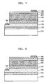
- the light emitting device may have a structure in which an electrode layer 220 is formed between the contact layer 230 and the p-cladding layer 150.
- the electrode layer 220 may be composed of an alloy or solid solution of one or two elements selected from the group consisting of Ni, Au, Pt, Pd, Mg, Cu, Zn, Ag, Sc, Co, Rh, Li, Be, Ca, Ru, Re, Ti Ta, Na, and La. Since the elements constituting the electrode layer 220 can adjust the concentration of p-type Zn-containing oxide, it may be advantageous to form a p-GaN ohmic contact.
- the light emitting device according to the present invention may also have a structure in which the electrode layer 220 is formed on the contact layer 230.
- the electrode layer 220 may be made of the materials described earlier with reference to FIG. 7 .
- FIG. 9 shows, in accordance with the present invention, an example of a light emitting device in which a reflective layer 240 is formed on the contact layer 230.
- the reflective layer 240 may be made of a metal selected from the group consisting of Ag, Al, Zn, Mg, Ru, Ti, Rh, Cr, and Pt.
- the light emitting device may have a structure in which the electrode layer 220, the contact layer 230, and the reflective layer 240 are sequentially formed on the p-cladding layer 150.
- the electrode layer 220 is composed of an alloy or solid solution of one or two elements selected from Ni, Au, Pt, Pd, Mg, Cu, Zn, Ag, Sc, Co, Rh, Li, Be, Ca, Ru, Re, Ti, Ta, Na, and La. Since the elements constituting the electrode layer 220 can adjust the concentration of p-type Zn-containing oxide, it may be advantageous to form a p-GaN ohmic contact.
- the reflective layer 240 may be made of a metal selected from the group consisting of Ag, Al, Zn, Mg, Ru, Ti, Rh, Cr, and Pt.
- the light emitting device may also have a structure in which the contact layer 230, the electrode layer 220, and the reflective layer 240 are sequentially formed on the p-cladding layer 150.
- the electrode layer 220 and the reflective layer 240 may each be composed of the materials described earlier with reference to FIG. 10 .
- FIG. 12 is a graph showing operating voltages respectively measured in InGaN/GaN MQW blue LEDs with a p-ZnO electrode structure having a single contact layer 230, which is similar to the electrode structure shown in FIG. 5 , and with a p-ZnO/Ag electrode structure, including a contact layer 230 and a reflective layer 240, which is similar to the electrode structure shown in FIG. 9 .
- annealing was performed at 530°C in an air atmosphere.
- the thickness of the single contact layer in the p-ZnO electrode structure was 300 nm, and the thicknesses of the contact layer 230 and the reflective layer 240 in the p-ZnO/Ag electrode structure were 100 nm and 200 nm, respectively.
- operating voltages of the light emitting devices with the p-ZnO electrode structure and the p-ZnO/Ag electrode structure are 3.33 V and 3.23 V, respectively, which are lower than an operating voltage of 3. 45 V in a conventional Ni/Au electrode structure.
- FIG. 13 is a graph showing operating voltages respectively measured in InGaN/GaN MQW ultraviolet (UV) LEDs with the same p-electrode structures as those used to obtain the results shown in FIG. 12 .
- the operating voltages of the light emitting devices with the p-ZnO and p-ZnO/Ag electrode structures were 3.67 V and 3.54 V at 20 mA, respectively.
- the light emitting devices have high operating voltages, it is expected that the above-described structures can be used to realize a light emitting device with good operating voltage characteristics in view of the results achieved during the initial phase of the development of UV LEDs.
- FIG. 14 is a graph showing relationships between operating voltages and output powers measured after annealing InGaN/GaN MQW blue LEDs with a p-ZnO electrode structure, which is similar to the structure shown in FIG. 1 , a p-ZnO/Ag electrode structure, which is similar to the structure shown in FIG. 2 , and a conventional Ni/Au electrode structure in air ambient.
- the p-ZnO and p-ZnO/Ag electrode structures can provide high equality light emitting devices with extremely low operating voltages and excellent output power that is four times higher than that obtained with the conventional Ni/Au electrode structure.
- a nitride-based light emitting device with a p-Mg x Zn 1-x O or p-Be x Zn 1-x O transparent film electrode and a method of fabricating the same according to the present invention provides excellent I-V characteristics by improving ohmic contact with a III-nitride-based p-cladding layer while significantly enhancing light emission efficiency of the device due to high light transmittance of the transparent electrode.
Landscapes
- Led Devices (AREA)
Claims (27)
- Nitrid-basierte lichtemittierende Vorrichtung, umfassend:ein Substrat (110);eine n-Mantelschicht (130), die auf dem Substrat angeordnet ist;eine aktive Schicht (140), die auf der n-Mantelschicht angeordnet ist;eine auf III-Nitrid-basierte p-Mantelschicht (150), die auf der aktiven Schicht angeordnet ist, sowieeine Kontaktschicht (230), die aus einem Zink (Zn) enthaltenden Oxid besteht, umfassend ein Dotiermittel vom p-Typ angeordnet auf der p-Mantelschicht zur Erzeugung eines ohmschen Kontaktes zur p-Mantelschicht; dadurch gekennzeichnet, dassdas Zn-enthaltende Oxid eine ternäre Verbindung ausgewählt aus der Gruppe bestehend aus MgxZn1-xO und BexZn1-xO ist.
- Lichtemittierende Vorrichtung nach Anspruch 1, wobei das Dotiermittel vom p-Typ wenigstens eines ausgewählt aus der Gruppe bestehend aus Phosphor (P) und Stickstoff (N) umfasst.
- Lichtemittierende Vorrichtung nach einem der vorangehenden Ansprüche, wobei die Konzentration des im Zn-enthaltenden Oxid enthaltenen Dotiermittels vom p-Typ im Bereich von 0,01 bis 30 Gew.-% liegt.
- Lichtemittierende Vorrichtung nach einem der vorangehenden Ansprüche, wobei die Kontaktschicht (230) in einer Dicke von 0,1 bis 1.000 nm ausgebildet ist.
- Lichtemittierende Vorrichtung nach einem der vorangehenden Ansprüche, ferner umfassend ein Saphirsubstrat (110) oder ein Siliziumcarbit (SiC)-Substrat (110) unter der n-Mantelschicht.
- Lichtemittierende Vorrichtung nach einem der vorangehenden Ansprüche, ferner umfassend eine reflektierende Schicht (240), die aus wenigstens einem Element ausgewählt aus der Gruppe bestehend aus Ag, Al, Zn, Mg, Ru, Ti, Rh, Cr und Pt besteht und auf der Kontaktschicht ausgebildet ist.
- Lichtemittierende Vorrichtung nach Anspruch 6, wobei die reflektierende Schicht (240) in einer Dicke von 10 bis 2.000 nm ausgebildet ist.
- Lichtemittierende Vorrichtung nach Anspruch 6 oder 7, ferner umfassend eine zweite Elektrodenschicht (220), die aus wenigstens einem Element ausgewählt aus der Gruppe bestehend aus Ni, Au, Pt, Pd, Mg, Cu, Zn, Ag, Sc, Co, Rh, Li, Be, Ca, Ru, Re, Ti, Ta, Na, und La besteht und die zwischen der Kontaktschicht (230) und der reflektierenden Schicht (240) angeordnet ist.
- Lichtemittierende Vorrichtung nach einem der vorangehenden Ansprüche, ferner umfassend eine erste Elektrodenschicht (220), die aus wenigstens einem Element ausgewählt aus der Gruppe bestehend aus Ni, Au, Pt, Pd, Mg, Cu, Zn, Ag, Sc, Co, Rh, Li, Be, Ca, Ru, Re, Ti, Ta, Na, und La besteht und die zwischen der p-Mantelschicht (150) und der Kontaktschicht (230) angeordnet ist.
- Verfahren zur Herstellung einer Nitrid-basierten lichtemittierenden Vorrichtung, bei der wenigstens eine n-Mantelschicht (130), eine aktive Schicht (140), und eine III-Nitrid-basierte p-Mantelschicht (150) der Reihe nach auf einem Substrat (110) ausgebildet sind, wobei das Verfahren Folgendes umfasst:Ausbilden einer Kontaktschicht (230) bestehend aus einem Zn-enthaltenden Oxid umfassend ein Dotiermittel vom p-Typ auf der p-Mantelschicht; sowieTempern der resultierenden Anordnung, die durch das Ausbilden der Kontaktschicht erhalten wurde, um einen ohmschen Kontakt zwischen der Kontaktschicht und der p-Mantelschicht zu bilden;wobei das Zn-enthaltende Oxid eine ternäre Verbindung ausgewählt aus der Gruppe bestehend aus MgxZn1-xO und BexZn1-xO ist; undwobei die Kontaktschicht (230) unter Verwendung eines ausgewählt aus der Gruppe bestehend aus Elektronenstrahlverdampfer, Sputterdeposition und Laserstrahlverdampfen ausgebildet ist.
- Verfahren nach Anspruch 10, wobei das Dotiermittel vom p-Typ wenigstens eines ausgewählt aus der Gruppe bestehend aus Phosphor (P) und Stickstoff (N) umfasst.
- Verfahren nach einem der Ansprüche 10 bis 11, wobei die aktive Schicht (140) eine InGaN/GaN-Multi-Quantum-Well (MQW)- oder AlGaN/GaN MQW-Struktur aufweist.
- Verfahren nach einem der Ansprüche 10 bis 12, wobei die Konzentration des im Zn-enthaltenden Oxids enthaltenden Dotiermittels vom p-Typ im Bereich von 0,01 bis 30 Gew.-% liegt.
- Verfahren nach einem der Ansprüche 10 bis 13, wobei die Kontaktschicht (230) in einer Dicke von 0,1 bis 1.000 nm ausgebildet ist.
- Verfahren nach Anspruch 10, wobei die Temperatur während der Abscheidung der Kontaktschicht (230) im Bereich von 20 bis 1.500 °C liegt und der Druck während der Deposition im Bereich von atmosphärischem Druck bis 1.33x10⁻¹⁰Pa (10-12 Torr) liegt.
- Verfahren nach einem der Ansprüche 10 bis 15, ferner umfassend das Ausbilden einer n-Strom-Blockierungsschicht (160) auf der p-Mantelschicht bevor die Kontaktschicht (230) ausgebildet ist.
- Verfahren nach Anspruch 16, wobei die n-Strom-Blockierungsschicht (160) in einer Dicke von 0,1 bis 500 nm ausgebildet ist.
- Verfahren nach Anspruch 16 bis 17, wobei die n-Strom-Blockierungsschicht (160) aus einem transparenten leitfähigen Oxid oder einer auf n-GaN-basierten Verbindung zusammengesetzt ist.
- Verfahren nach Anspruch 18, wobei die n-Strom-Blockierungsschicht (160) ein transparentes leitfähiges Oxid ist ausgewählt aus der Gruppe bestehend aus In2O3, SnO2, und Indiumzinnoxid (ITO).
- Verfahren nach einem der Ansprüche 10 bis 19, ferner umfassend, vor dem Ausbilden der Kontaktschicht, das Ausbilden einer ersten Elektrodenschicht (220) auf der p-Mantelschicht (150) aus wenigstens einem Element ausgewählt aus der Gruppe bestehend aus Ni, Au, Pt, Pd, Mg, Cu, Zn, Ag, Sc, Co, Rh, Li, Be, Ca, Ru, Re, Ti, Ta, Na und La.
- Verfahren nach einem der Ansprüche 10 bis 20, ferner umfassend, vor dem Tempern, das Ausbilden einer zweiten Elektrodenschicht (220) auf der Kontaktschicht aus wenigstens einem Element ausgewählt aus der Gruppe bestehend aus Ni, Au, Pt, Pd, Mg, Cu, Zn, Ag, Sc, Co, Rh, Li, Be, Ca, Ru, Re, Ti, Ta, Na und La.
- Verfahren nach Anspruch 20, wobei die erste Elektrodenschicht (220) in einer Dicke von 0,1 bis 1,000 nm ausgebildet ist.
- Verfahren nach einem der Ansprüche 10 bis 22, ferner umfassend, vor dem Tempern, das Ausbilden einer reflektierenden Schicht (240) auf der Kontaktschicht aus wenigstens einem Element ausgewählt aus der Gruppe bestehend aus Ag, Al, Zn, Mg, Ru, Ti, Rh, Cr und Pt.
- Verfahren nach Anspruch 23, wobei die reflektierende Schicht (240) in einer Dicke von 10 bis 2.000 nm ausgebildet ist.
- Verfahren nach einem der Ansprüche 10 bis 24, wobei das Tempern bei einer Temperatur von 100 bis 800 °C durchgeführt wird.
- Verfahren nach einem der Ansprüche 10 bis 25, wobei das Tempern 10 Sekunden bis 3 Stunden lang durchgeführt wird.
- Verfahren nach einem der Ansprüche 10 bis 26, wobei das Tempern in einer gasartigen Atmosphäre enthaltend wenigstens eines aus N2, Ar, He, O2, H und Luft durchgeführt wird.
Priority Applications (1)
| Application Number | Priority Date | Filing Date | Title |
|---|---|---|---|
| EP10181626A EP2262013B1 (de) | 2003-10-08 | 2004-10-05 | Verfahren zur Herstellung einer Galliumnitrid-basierten lichtemittierenden Diode |
Applications Claiming Priority (2)
| Application Number | Priority Date | Filing Date | Title |
|---|---|---|---|
| KR2003069995 | 2003-10-08 | ||
| KR1020030069995A KR100571818B1 (ko) | 2003-10-08 | 2003-10-08 | 질화물계 발광소자 및 그 제조방법 |
Related Child Applications (2)
| Application Number | Title | Priority Date | Filing Date |
|---|---|---|---|
| EP10181626A Division-Into EP2262013B1 (de) | 2003-10-08 | 2004-10-05 | Verfahren zur Herstellung einer Galliumnitrid-basierten lichtemittierenden Diode |
| EP10181626A Division EP2262013B1 (de) | 2003-10-08 | 2004-10-05 | Verfahren zur Herstellung einer Galliumnitrid-basierten lichtemittierenden Diode |
Publications (3)
| Publication Number | Publication Date |
|---|---|
| EP1523047A2 EP1523047A2 (de) | 2005-04-13 |
| EP1523047A3 EP1523047A3 (de) | 2006-11-22 |
| EP1523047B1 true EP1523047B1 (de) | 2012-09-26 |
Family
ID=34309562
Family Applications (2)
| Application Number | Title | Priority Date | Filing Date |
|---|---|---|---|
| EP10181626A Expired - Lifetime EP2262013B1 (de) | 2003-10-08 | 2004-10-05 | Verfahren zur Herstellung einer Galliumnitrid-basierten lichtemittierenden Diode |
| EP04256154A Expired - Lifetime EP1523047B1 (de) | 2003-10-08 | 2004-10-05 | Nitrid-basierte lichtemittierende Halbleitervorrichtung und Herstellungsverfahren dafür |
Family Applications Before (1)
| Application Number | Title | Priority Date | Filing Date |
|---|---|---|---|
| EP10181626A Expired - Lifetime EP2262013B1 (de) | 2003-10-08 | 2004-10-05 | Verfahren zur Herstellung einer Galliumnitrid-basierten lichtemittierenden Diode |
Country Status (5)
| Country | Link |
|---|---|
| US (2) | US7180094B2 (de) |
| EP (2) | EP2262013B1 (de) |
| JP (1) | JP5253704B2 (de) |
| KR (1) | KR100571818B1 (de) |
| CN (1) | CN1606177B (de) |
Families Citing this family (77)
| Publication number | Priority date | Publication date | Assignee | Title |
|---|---|---|---|---|
| KR100624411B1 (ko) * | 2003-08-25 | 2006-09-18 | 삼성전자주식회사 | 질화물계 발광소자 및 그 제조방법 |
| DE102004026231B4 (de) | 2004-05-28 | 2019-01-31 | Osram Opto Semiconductors Gmbh | Verfahren zur Herstellung eines Bereichs mit reduzierter elektrischer Leitfähigkeit innerhalb einer Halbleiterschicht und optoelektronisches Halbleiterbauelement |
| KR100700006B1 (ko) * | 2004-11-23 | 2007-03-26 | 삼성에스디아이 주식회사 | 유기 전계 발광 표시 소자 및 그 제조방법 |
| KR20080014727A (ko) | 2004-12-27 | 2008-02-14 | 퀀덤 페이퍼, 인크. | 어드레스 가능 및 프린트 가능 발광 디스플레이 |
| KR100638813B1 (ko) * | 2005-04-15 | 2006-10-27 | 삼성전기주식회사 | 플립칩형 질화물 반도체 발광소자 |
| DE102005046190A1 (de) | 2005-09-27 | 2007-04-05 | Osram Opto Semiconductors Gmbh | Optoelektronisches Halbleiterbauelement mit Stromaufweitungsschicht |
| KR100784382B1 (ko) * | 2005-12-16 | 2007-12-11 | 삼성전자주식회사 | 광학 소자 및 그 제조 방법 |
| US8487344B2 (en) | 2005-12-16 | 2013-07-16 | Samsung Display Co., Ltd. | Optical device and method of fabricating the same |
| JP4655920B2 (ja) * | 2005-12-22 | 2011-03-23 | 日立電線株式会社 | 半導体発光素子 |
| KR100784384B1 (ko) * | 2005-12-27 | 2007-12-11 | 삼성전자주식회사 | 광학 소자 및 그 제조방법 |
| JP5244614B2 (ja) | 2005-12-27 | 2013-07-24 | 三星ディスプレイ株式會社 | Iii族窒化物系発光素子 |
| DE102006034847A1 (de) * | 2006-04-27 | 2007-10-31 | Osram Opto Semiconductors Gmbh | Optoelektronischer Halbleiterchip |
| KR100809243B1 (ko) * | 2006-04-27 | 2008-02-29 | 삼성전기주식회사 | 질화물막 제조방법 및 질화물 구조 |
| US7501295B2 (en) * | 2006-05-25 | 2009-03-10 | Philips Lumileds Lighting Company, Llc | Method of fabricating a reflective electrode for a semiconductor light emitting device |
| TWI306316B (en) * | 2006-07-28 | 2009-02-11 | Huga Optotech Inc | Semiconductor light emitting device and method of fabricating the same |
| TWI325641B (en) | 2006-09-04 | 2010-06-01 | Huga Optotech Inc | Light emitting device and methods for forming the same |
| KR101262386B1 (ko) * | 2006-09-25 | 2013-05-08 | 엘지이노텍 주식회사 | 질화물 반도체 발광소자의 제조 방법 |
| WO2008045423A1 (en) * | 2006-10-10 | 2008-04-17 | Structured Materials Inc. | Self assembled controlled luminescent transparent conductive photonic crystals for light emitting devices |
| JP5072397B2 (ja) * | 2006-12-20 | 2012-11-14 | 昭和電工株式会社 | 窒化ガリウム系化合物半導体発光素子およびその製造方法 |
| GB2446611B (en) * | 2007-02-14 | 2011-08-17 | Bookham Technology Plc | Low creep metallization for optoelectronic applications |
| FR2914496B1 (fr) * | 2007-03-29 | 2009-10-02 | Soitec Silicon On Insulator | Amelioration de la defectivite post decollement d'une couche mince par modification de son recuit de decollement. |
| US9018833B2 (en) | 2007-05-31 | 2015-04-28 | Nthdegree Technologies Worldwide Inc | Apparatus with light emitting or absorbing diodes |
| US8877101B2 (en) | 2007-05-31 | 2014-11-04 | Nthdegree Technologies Worldwide Inc | Method of manufacturing a light emitting, power generating or other electronic apparatus |
| US8384630B2 (en) | 2007-05-31 | 2013-02-26 | Nthdegree Technologies Worldwide Inc | Light emitting, photovoltaic or other electronic apparatus and system |
| US7972031B2 (en) * | 2007-05-31 | 2011-07-05 | Nthdegree Technologies Worldwide Inc | Addressable or static light emitting or electronic apparatus |
| US8809126B2 (en) | 2007-05-31 | 2014-08-19 | Nthdegree Technologies Worldwide Inc | Printable composition of a liquid or gel suspension of diodes |
| US8889216B2 (en) | 2007-05-31 | 2014-11-18 | Nthdegree Technologies Worldwide Inc | Method of manufacturing addressable and static electronic displays |
| US8133768B2 (en) | 2007-05-31 | 2012-03-13 | Nthdegree Technologies Worldwide Inc | Method of manufacturing a light emitting, photovoltaic or other electronic apparatus and system |
| US8674593B2 (en) | 2007-05-31 | 2014-03-18 | Nthdegree Technologies Worldwide Inc | Diode for a printable composition |
| US9425357B2 (en) | 2007-05-31 | 2016-08-23 | Nthdegree Technologies Worldwide Inc. | Diode for a printable composition |
| US9419179B2 (en) | 2007-05-31 | 2016-08-16 | Nthdegree Technologies Worldwide Inc | Diode for a printable composition |
| US9534772B2 (en) | 2007-05-31 | 2017-01-03 | Nthdegree Technologies Worldwide Inc | Apparatus with light emitting diodes |
| US8852467B2 (en) | 2007-05-31 | 2014-10-07 | Nthdegree Technologies Worldwide Inc | Method of manufacturing a printable composition of a liquid or gel suspension of diodes |
| US8846457B2 (en) | 2007-05-31 | 2014-09-30 | Nthdegree Technologies Worldwide Inc | Printable composition of a liquid or gel suspension of diodes |
| US9343593B2 (en) | 2007-05-31 | 2016-05-17 | Nthdegree Technologies Worldwide Inc | Printable composition of a liquid or gel suspension of diodes |
| US8415879B2 (en) | 2007-05-31 | 2013-04-09 | Nthdegree Technologies Worldwide Inc | Diode for a printable composition |
| WO2009026749A1 (en) * | 2007-08-31 | 2009-03-05 | Lattice Power (Jiangxi) Corporation | Method for fabricating a low-resistivity ohmic contact to a p-type iii-v nitride semiconductor material at low temperature |
| TW200939510A (en) * | 2007-11-19 | 2009-09-16 | Applied Materials Inc | Solar cell contact formation process using a patterned etchant material |
| US20090139568A1 (en) * | 2007-11-19 | 2009-06-04 | Applied Materials, Inc. | Crystalline Solar Cell Metallization Methods |
| CN101960603A (zh) * | 2008-01-08 | 2011-01-26 | 莫克斯特尼克公司 | 高性能异质结构发光装置及方法 |
| CN102036999A (zh) * | 2008-03-21 | 2011-04-27 | 内诺格雷姆公司 | 金属硅氮化物或金属硅氧氮化物亚微米荧光粉颗粒及合成这些荧光粉的方法 |
| WO2009126010A2 (ko) * | 2008-04-12 | 2009-10-15 | 엘지이노텍주식회사 | 발광 소자 |
| KR101007099B1 (ko) | 2008-04-21 | 2011-01-10 | 엘지이노텍 주식회사 | 반도체 발광소자 및 그 제조방법 |
| US7992332B2 (en) | 2008-05-13 | 2011-08-09 | Nthdegree Technologies Worldwide Inc. | Apparatuses for providing power for illumination of a display object |
| US8127477B2 (en) | 2008-05-13 | 2012-03-06 | Nthdegree Technologies Worldwide Inc | Illuminating display systems |
| CN102099976B (zh) | 2008-05-30 | 2013-06-12 | 加利福尼亚大学董事会 | 在降低的温度下制造的(Al、Ga、In)N二极管激光器 |
| WO2010009297A2 (en) | 2008-07-16 | 2010-01-21 | Applied Materials, Inc. | Hybrid heterojunction solar cell fabrication using a doping layer mask |
| EP2324509A2 (de) * | 2008-08-27 | 2011-05-25 | Applied Materials, Inc. | Rückseitenkontakt-solarzellen mit gedruckter dielektrischer barriere |
| US9711688B2 (en) | 2008-12-02 | 2017-07-18 | Koninklijke Philips N.V. | Controlling LED emission pattern using optically active materials |
| KR100992743B1 (ko) * | 2008-12-26 | 2010-11-05 | 엘지이노텍 주식회사 | 발광소자 및 그 제조방법 |
| JP5258707B2 (ja) | 2009-08-26 | 2013-08-07 | 株式会社東芝 | 半導体発光素子 |
| KR101020963B1 (ko) * | 2010-04-23 | 2011-03-09 | 엘지이노텍 주식회사 | 발광 소자, 발광 소자 제조방법 및 발광 소자 패키지 |
| US9190560B2 (en) * | 2010-05-18 | 2015-11-17 | Agency For Science Technology And Research | Method of forming a light emitting diode structure and a light diode structure |
| JP4940363B1 (ja) | 2011-02-28 | 2012-05-30 | 株式会社東芝 | 半導体発光素子及び半導体発光装置 |
| JP2012186195A (ja) * | 2011-03-03 | 2012-09-27 | Toshiba Corp | 半導体発光素子及びその製造方法 |
| JP5479391B2 (ja) * | 2011-03-08 | 2014-04-23 | 株式会社東芝 | 半導体発光素子及びその製造方法 |
| KR101395432B1 (ko) * | 2011-07-28 | 2014-05-14 | 주식회사 막스 | 백색 led 장치 |
| JP2013120829A (ja) * | 2011-12-07 | 2013-06-17 | Sharp Corp | 窒化物半導体紫外発光素子 |
| US9818912B2 (en) | 2011-12-12 | 2017-11-14 | Sensor Electronic Technology, Inc. | Ultraviolet reflective contact |
| EP2791983A4 (de) | 2011-12-12 | 2015-08-12 | Sensor Electronic Tech Inc | Uv-reflexionskontakt |
| CN104011882A (zh) | 2012-01-12 | 2014-08-27 | 应用材料公司 | 制造太阳能电池装置的方法 |
| KR101335045B1 (ko) * | 2012-10-16 | 2013-11-29 | 엘지전자 주식회사 | 발광 다이오드 |
| CN103247607B (zh) * | 2012-10-19 | 2016-01-20 | 璨圆光电股份有限公司 | 发光二极管 |
| US9768357B2 (en) | 2013-01-09 | 2017-09-19 | Sensor Electronic Technology, Inc. | Ultraviolet reflective rough adhesive contact |
| WO2014110197A1 (en) | 2013-01-09 | 2014-07-17 | Sensor Electronic Technology, Inc. | Ultraviolet reflective rough adhesive contact |
| US10276749B2 (en) | 2013-01-09 | 2019-04-30 | Sensor Electronic Technology, Inc. | Ultraviolet reflective rough adhesive contact |
| US9202875B2 (en) * | 2014-02-18 | 2015-12-01 | Taiwan Semiconductor Manufacturing Company, Ltd. | High electron mobility transistor with indium nitride layer |
| DE102014107306A1 (de) * | 2014-05-23 | 2015-11-26 | Osram Opto Semiconductors Gmbh | Verfahren zur Herstellung eines optoelektronischen Halbleiterchips und optoelektronischer Halbleiterchip |
| WO2019031745A2 (ko) * | 2017-08-11 | 2019-02-14 | 서울바이오시스주식회사 | 발광 다이오드 |
| KR102499308B1 (ko) | 2017-08-11 | 2023-02-14 | 서울바이오시스 주식회사 | 발광 다이오드 |
| US11393955B2 (en) | 2018-08-03 | 2022-07-19 | Genesis Photonics Inc. | Light emitting diode and manufacturing method thereof |
| CN110797444B (zh) * | 2018-08-03 | 2022-10-28 | 新世纪光电股份有限公司 | 发光二极管芯片与发光二极管装置 |
| CN109346562A (zh) * | 2018-08-30 | 2019-02-15 | 华灿光电(浙江)有限公司 | 一种发光二极管外延片的制备方法及发光二极管外延片 |
| KR102218587B1 (ko) | 2019-08-09 | 2021-02-22 | 순천대학교 산학협력단 | 반도체 발광소자의 제조 방법 및 반도체 발광소자 |
| CN112768582B (zh) * | 2021-02-26 | 2022-03-25 | 南京大学 | 包含高反射n-GaN欧姆接触的倒装LED芯片及其制作方法 |
| WO2025023585A1 (ko) * | 2023-07-25 | 2025-01-30 | 한국광기술원 | 우수한 광효율을 갖는 발광소자 및 그의 제조방법 |
| TWI898845B (zh) * | 2023-09-25 | 2025-09-21 | 韓國光技術院 | 發光元件及其製造方法 |
Family Cites Families (17)
| Publication number | Priority date | Publication date | Assignee | Title |
|---|---|---|---|---|
| EP0408373B1 (de) * | 1989-07-12 | 2000-04-26 | Kabushiki Kaisha Toshiba | Im transversalen Mode schwingender Halbleiterlaser |
| JP3009095B2 (ja) * | 1995-10-27 | 2000-02-14 | 日亜化学工業株式会社 | 窒化物半導体発光素子 |
| US5889295A (en) * | 1996-02-26 | 1999-03-30 | Kabushiki Kaisha Toshiba | Semiconductor device |
| JP3304787B2 (ja) * | 1996-09-08 | 2002-07-22 | 豊田合成株式会社 | 半導体発光素子及びその製造方法 |
| JP3736181B2 (ja) * | 1998-05-13 | 2006-01-18 | 豊田合成株式会社 | Iii族窒化物系化合物半導体発光素子 |
| JP2000294837A (ja) * | 1999-04-05 | 2000-10-20 | Stanley Electric Co Ltd | 窒化ガリウム系化合物半導体発光素子 |
| US6287947B1 (en) | 1999-06-08 | 2001-09-11 | Lumileds Lighting, U.S. Llc | Method of forming transparent contacts to a p-type GaN layer |
| JP3068914U (ja) * | 1999-11-11 | 2000-05-26 | 洲磊科技股▲ふん▼有限公司 | フリップ―チップ発光デバイス |
| JP4024994B2 (ja) | 2000-06-30 | 2007-12-19 | 株式会社東芝 | 半導体発光素子 |
| JP3904378B2 (ja) * | 2000-08-02 | 2007-04-11 | ローム株式会社 | 酸化亜鉛透明導電膜 |
| AU2001285055A1 (en) * | 2000-08-18 | 2002-03-04 | Midwest Research Institute | High carrier concentration p-type transparent conducting oxide films |
| JP2002164570A (ja) * | 2000-11-24 | 2002-06-07 | Shiro Sakai | 窒化ガリウム系化合物半導体装置 |
| JP3697609B2 (ja) | 2001-05-23 | 2005-09-21 | 日立電線株式会社 | 半導体発光素子 |
| TW513820B (en) * | 2001-12-26 | 2002-12-11 | United Epitaxy Co Ltd | Light emitting diode and its manufacturing method |
| JP3795007B2 (ja) * | 2002-11-27 | 2006-07-12 | 松下電器産業株式会社 | 半導体発光素子及びその製造方法 |
| KR20050051920A (ko) * | 2003-11-28 | 2005-06-02 | 삼성전자주식회사 | 플립칩형 질화물계 발광소자 및 그 제조방법 |
| US20070267646A1 (en) * | 2004-06-03 | 2007-11-22 | Philips Lumileds Lighting Company, Llc | Light Emitting Device Including a Photonic Crystal and a Luminescent Ceramic |
-
2003
- 2003-10-08 KR KR1020030069995A patent/KR100571818B1/ko not_active Expired - Fee Related
-
2004
- 2004-10-01 JP JP2004290424A patent/JP5253704B2/ja not_active Expired - Fee Related
- 2004-10-05 US US10/957,704 patent/US7180094B2/en not_active Expired - Lifetime
- 2004-10-05 EP EP10181626A patent/EP2262013B1/de not_active Expired - Lifetime
- 2004-10-05 EP EP04256154A patent/EP1523047B1/de not_active Expired - Lifetime
- 2004-10-08 CN CN200410092115.4A patent/CN1606177B/zh not_active Expired - Lifetime
-
2007
- 2007-01-04 US US11/649,236 patent/US7485479B2/en not_active Expired - Lifetime
Non-Patent Citations (1)
| Title |
|---|
| KO Y.-D. ET AL.: "Characteristics of ZnO/Si prepared by Zn3P2 diffusion", APPLIED SURFACE SCIENCE, vol. 202, 30 December 2002 (2002-12-30), pages 266 - 271 * |
Also Published As
| Publication number | Publication date |
|---|---|
| EP1523047A2 (de) | 2005-04-13 |
| US7485479B2 (en) | 2009-02-03 |
| CN1606177B (zh) | 2010-05-26 |
| US20050077537A1 (en) | 2005-04-14 |
| US20070111354A1 (en) | 2007-05-17 |
| EP1523047A3 (de) | 2006-11-22 |
| KR20050034155A (ko) | 2005-04-14 |
| CN1606177A (zh) | 2005-04-13 |
| EP2262013B1 (de) | 2012-09-19 |
| JP2005117040A (ja) | 2005-04-28 |
| US7180094B2 (en) | 2007-02-20 |
| JP5253704B2 (ja) | 2013-07-31 |
| EP2262013A2 (de) | 2010-12-15 |
| EP2262013A3 (de) | 2011-06-15 |
| KR100571818B1 (ko) | 2006-04-17 |
Similar Documents
| Publication | Publication Date | Title |
|---|---|---|
| US7485479B2 (en) | Nitride-based light emitting device and method of manufacturing the same | |
| US7485897B2 (en) | Nitride-based light-emitting device having grid cell layer | |
| US8395176B2 (en) | Top-emitting nitride-based light-emitting device with ohmic characteristics and luminous efficiency | |
| US7193249B2 (en) | Nitride-based light emitting device and method of manufacturing the same | |
| US7491979B2 (en) | Reflective electrode and compound semiconductor light emitting device including the same | |
| EP1531499A2 (de) | Nitrid lichtemittierende Halbleitervorrichtung und Herstellungsverfahren | |
| KR100571816B1 (ko) | 질화물계 발광소자 및 그 제조방법 | |
| US20050167681A1 (en) | Electrode layer, light emitting device including the same, and method of forming the electrode layer | |
| JP5220409B2 (ja) | トップエミット型窒化物系発光素子の製造方法 | |
| KR20060007948A (ko) | 탑에미트형 질화물계 발광소자 및 그 제조방법 | |
| KR100764458B1 (ko) | 전극층, 이를 구비하는 발광소자 및 전극층 제조방법 | |
| KR100611642B1 (ko) | 탑에미트형 질화물계 발광소자 및 그 제조방법 | |
| KR100611640B1 (ko) | 플립칩형 질화물계 발광소자 및 그 제조방법 | |
| KR100611639B1 (ko) | 탑에미트형 질화물계 발광소자 및 그 제조방법 | |
| KR100574104B1 (ko) | 플립칩형 질화물계 발광소자 및 그 제조방법 | |
| KR100574103B1 (ko) | 플립칩형 질화물계 발광소자 및 그 제조방법 | |
| KR100574102B1 (ko) | 플립칩형 질화물계 발광소자 및 그 제조방법 |
Legal Events
| Date | Code | Title | Description |
|---|---|---|---|
| PUAI | Public reference made under article 153(3) epc to a published international application that has entered the european phase |
Free format text: ORIGINAL CODE: 0009012 |
|
| AK | Designated contracting states |
Kind code of ref document: A2 Designated state(s): AT BE BG CH CY CZ DE DK EE ES FI FR GB GR HU IE IT LI LU MC NL PL PT RO SE SI SK TR |
|
| AX | Request for extension of the european patent |
Extension state: AL HR LT LV MK |
|
| PUAL | Search report despatched |
Free format text: ORIGINAL CODE: 0009013 |
|
| AK | Designated contracting states |
Kind code of ref document: A3 Designated state(s): AT BE BG CH CY CZ DE DK EE ES FI FR GB GR HU IE IT LI LU MC NL PL PT RO SE SI SK TR |
|
| AX | Request for extension of the european patent |
Extension state: AL HR LT LV MK |
|
| 17P | Request for examination filed |
Effective date: 20070321 |
|
| AKX | Designation fees paid |
Designated state(s): DE FR GB |
|
| 17Q | First examination report despatched |
Effective date: 20070709 |
|
| RAP1 | Party data changed (applicant data changed or rights of an application transferred) |
Owner name: GWANGJU INSTITUTE OF SCIENCE AND TECHNOLOGY Owner name: SAMSUNG LED CO., LTD. |
|
| REG | Reference to a national code |
Ref country code: DE Ref legal event code: R079 Ref document number: 602004039445 Country of ref document: DE Free format text: PREVIOUS MAIN CLASS: H01L0033000000 Ipc: H01L0033420000 |
|
| RIC1 | Information provided on ipc code assigned before grant |
Ipc: H01L 33/42 20100101AFI20120328BHEP Ipc: H01L 33/32 20100101ALN20120328BHEP |
|
| RTI1 | Title (correction) |
Free format text: NITRIDE-BASED SEMICONDUCTOR LIGHT EMITTING DEVICE AND METHOD OF MANUFACTURING THE SAME |
|
| GRAP | Despatch of communication of intention to grant a patent |
Free format text: ORIGINAL CODE: EPIDOSNIGR1 |
|
| RIC1 | Information provided on ipc code assigned before grant |
Ipc: H01L 33/42 20100101AFI20120424BHEP Ipc: H01L 33/32 20100101ALN20120424BHEP |
|
| GRAS | Grant fee paid |
Free format text: ORIGINAL CODE: EPIDOSNIGR3 |
|
| GRAA | (expected) grant |
Free format text: ORIGINAL CODE: 0009210 |
|
| AK | Designated contracting states |
Kind code of ref document: B1 Designated state(s): DE FR GB |
|
| REG | Reference to a national code |
Ref country code: GB Ref legal event code: FG4D |
|
| REG | Reference to a national code |
Ref country code: DE Ref legal event code: R096 Ref document number: 602004039445 Country of ref document: DE Effective date: 20121122 |
|
| REG | Reference to a national code |
Ref country code: GB Ref legal event code: 732E Free format text: REGISTERED BETWEEN 20121129 AND 20121205 |
|
| REG | Reference to a national code |
Ref country code: DE Ref legal event code: R081 Ref document number: 602004039445 Country of ref document: DE Owner name: SAMSUNG ELECTRONICS CO., LTD., KR Free format text: FORMER OWNER: SAMSUNG ELECTRONICS CO., LTD., GWANGJU INSTITUTE OF SCIENCE AN, , KR Effective date: 20120926 Ref country code: DE Ref legal event code: R081 Ref document number: 602004039445 Country of ref document: DE Owner name: GWANGJU INSTITUTE OF SCIENCE AND TECHNOLOGY, KR Free format text: FORMER OWNER: SAMSUNG ELECTRONICS CO., LTD., GWANGJU INSTITUTE OF SCIENCE AN, , KR Effective date: 20120926 Ref country code: DE Ref legal event code: R081 Ref document number: 602004039445 Country of ref document: DE Owner name: SAMSUNG LED CO., LTD., KR Free format text: FORMER OWNER: SAMSUNG ELECTRONICS CO., LTD., GWANGJU INSTITUTE OF SCIENCE AN, , KR Effective date: 20120926 Ref country code: DE Ref legal event code: R081 Ref document number: 602004039445 Country of ref document: DE Owner name: SAMSUNG LED CO., LTD., SUWON, KR Free format text: FORMER OWNER: SAMSUNG ELECTRONICS CO., LTD., GWANGJU INSTITUTE OF SCIENCE AN, , KR Effective date: 20120926 Ref country code: DE Ref legal event code: R081 Ref document number: 602004039445 Country of ref document: DE Owner name: GWANGJU INSTITUTE OF SCIENCE AND TECHNOLOGY, KR Free format text: FORMER OWNERS: SAMSUNG ELECTRONICS CO., LTD., SUWON-SI, GYEONGGI-DO, KR; GWANGJU INSTITUTE OF SCIENCE AND TECHNOLOGY, GWANGJU, KR Effective date: 20120926 Ref country code: DE Ref legal event code: R081 Ref document number: 602004039445 Country of ref document: DE Owner name: SAMSUNG LED CO., LTD., SUWON, KR Free format text: FORMER OWNERS: SAMSUNG ELECTRONICS CO., LTD., SUWON-SI, GYEONGGI-DO, KR; GWANGJU INSTITUTE OF SCIENCE AND TECHNOLOGY, GWANGJU, KR Effective date: 20120926 Ref country code: DE Ref legal event code: R081 Ref document number: 602004039445 Country of ref document: DE Owner name: SAMSUNG ELECTRONICS CO., LTD., SUWON-SI, KR Free format text: FORMER OWNERS: SAMSUNG ELECTRONICS CO., LTD., SUWON-SI, GYEONGGI-DO, KR; GWANGJU INSTITUTE OF SCIENCE AND TECHNOLOGY, GWANGJU, KR Effective date: 20120926 |
|
| PLBE | No opposition filed within time limit |
Free format text: ORIGINAL CODE: 0009261 |
|
| STAA | Information on the status of an ep patent application or granted ep patent |
Free format text: STATUS: NO OPPOSITION FILED WITHIN TIME LIMIT |
|
| 26N | No opposition filed |
Effective date: 20130627 |
|
| REG | Reference to a national code |
Ref country code: FR Ref legal event code: ST Effective date: 20130805 |
|
| REG | Reference to a national code |
Ref country code: DE Ref legal event code: R097 Ref document number: 602004039445 Country of ref document: DE Effective date: 20130627 |
|
| PG25 | Lapsed in a contracting state [announced via postgrant information from national office to epo] |
Ref country code: FR Free format text: LAPSE BECAUSE OF NON-PAYMENT OF DUE FEES Effective date: 20121126 |
|
| REG | Reference to a national code |
Ref country code: DE Ref legal event code: R082 Ref document number: 602004039445 Country of ref document: DE Representative=s name: PATENTANWAELTE RUFF, WILHELM, BEIER, DAUSTER &, DE |
|
| P01 | Opt-out of the competence of the unified patent court (upc) registered |
Effective date: 20230524 |
|
| PGFP | Annual fee paid to national office [announced via postgrant information from national office to epo] |
Ref country code: GB Payment date: 20230824 Year of fee payment: 20 |
|
| PGFP | Annual fee paid to national office [announced via postgrant information from national office to epo] |
Ref country code: DE Payment date: 20230822 Year of fee payment: 20 |
|
| REG | Reference to a national code |
Ref country code: DE Ref legal event code: R071 Ref document number: 602004039445 Country of ref document: DE |
|
| REG | Reference to a national code |
Ref country code: GB Ref legal event code: PE20 Expiry date: 20241004 |
|
| PG25 | Lapsed in a contracting state [announced via postgrant information from national office to epo] |
Ref country code: GB Free format text: LAPSE BECAUSE OF EXPIRATION OF PROTECTION Effective date: 20241004 |
|
| PG25 | Lapsed in a contracting state [announced via postgrant information from national office to epo] |
Ref country code: GB Free format text: LAPSE BECAUSE OF EXPIRATION OF PROTECTION Effective date: 20241004 |