EP1524681A2 - Appareil à faisceau de particules avec section variable - Google Patents
Appareil à faisceau de particules avec section variable Download PDFInfo
- Publication number
- EP1524681A2 EP1524681A2 EP04077809A EP04077809A EP1524681A2 EP 1524681 A2 EP1524681 A2 EP 1524681A2 EP 04077809 A EP04077809 A EP 04077809A EP 04077809 A EP04077809 A EP 04077809A EP 1524681 A2 EP1524681 A2 EP 1524681A2
- Authority
- EP
- European Patent Office
- Prior art keywords
- aperture
- charged particle
- target
- edge
- rectangular
- Prior art date
- Legal status (The legal status is an assumption and is not a legal conclusion. Google has not performed a legal analysis and makes no representation as to the accuracy of the status listed.)
- Withdrawn
Links
- 238000000034 method Methods 0.000 title claims abstract description 31
- 230000004075 alteration Effects 0.000 claims abstract description 59
- 238000003801 milling Methods 0.000 claims abstract description 27
- 239000000463 material Substances 0.000 claims abstract description 12
- 239000002245 particle Substances 0.000 claims description 40
- 230000003287 optical effect Effects 0.000 claims description 32
- 238000003384 imaging method Methods 0.000 claims description 10
- 238000005096 rolling process Methods 0.000 claims 2
- 238000001514 detection method Methods 0.000 claims 1
- 238000004519 manufacturing process Methods 0.000 abstract description 3
- 238000010884 ion-beam technique Methods 0.000 description 25
- 150000002500 ions Chemical class 0.000 description 20
- 238000007493 shaping process Methods 0.000 description 10
- 238000004088 simulation Methods 0.000 description 10
- 238000013459 approach Methods 0.000 description 9
- 238000010586 diagram Methods 0.000 description 7
- 238000000151 deposition Methods 0.000 description 6
- 230000000694 effects Effects 0.000 description 6
- 230000006870 function Effects 0.000 description 6
- 230000008901 benefit Effects 0.000 description 5
- 230000008021 deposition Effects 0.000 description 4
- 238000009826 distribution Methods 0.000 description 4
- 230000004907 flux Effects 0.000 description 4
- 230000006872 improvement Effects 0.000 description 4
- 150000001875 compounds Chemical class 0.000 description 3
- 238000005520 cutting process Methods 0.000 description 3
- 238000005530 etching Methods 0.000 description 3
- 229910001338 liquidmetal Inorganic materials 0.000 description 3
- 230000008569 process Effects 0.000 description 3
- 238000006243 chemical reaction Methods 0.000 description 2
- 238000006073 displacement reaction Methods 0.000 description 2
- 230000009977 dual effect Effects 0.000 description 2
- 229910021645 metal ion Inorganic materials 0.000 description 2
- 239000000203 mixture Substances 0.000 description 2
- 239000004065 semiconductor Substances 0.000 description 2
- 239000000758 substrate Substances 0.000 description 2
- 238000013519 translation Methods 0.000 description 2
- GYHNNYVSQQEPJS-UHFFFAOYSA-N Gallium Chemical compound [Ga] GYHNNYVSQQEPJS-UHFFFAOYSA-N 0.000 description 1
- 108010083687 Ion Pumps Proteins 0.000 description 1
- 238000010521 absorption reaction Methods 0.000 description 1
- 230000001133 acceleration Effects 0.000 description 1
- 230000009286 beneficial effect Effects 0.000 description 1
- 230000005540 biological transmission Effects 0.000 description 1
- 238000001574 biopsy Methods 0.000 description 1
- 230000005465 channeling Effects 0.000 description 1
- 238000012790 confirmation Methods 0.000 description 1
- 238000010276 construction Methods 0.000 description 1
- 230000001627 detrimental effect Effects 0.000 description 1
- 239000010432 diamond Substances 0.000 description 1
- 230000002349 favourable effect Effects 0.000 description 1
- 229910052733 gallium Inorganic materials 0.000 description 1
- 238000010438 heat treatment Methods 0.000 description 1
- 230000000977 initiatory effect Effects 0.000 description 1
- 238000002347 injection Methods 0.000 description 1
- 239000007924 injection Substances 0.000 description 1
- 230000003993 interaction Effects 0.000 description 1
- 239000012528 membrane Substances 0.000 description 1
- 230000005055 memory storage Effects 0.000 description 1
- 238000002360 preparation method Methods 0.000 description 1
- 238000012545 processing Methods 0.000 description 1
- 238000005086 pumping Methods 0.000 description 1
- 239000000243 solution Substances 0.000 description 1
- 238000003860 storage Methods 0.000 description 1
- 238000006467 substitution reaction Methods 0.000 description 1
- 238000012546 transfer Methods 0.000 description 1
- 230000008016 vaporization Effects 0.000 description 1
Images


Classifications
-
- H—ELECTRICITY
- H01—ELECTRIC ELEMENTS
- H01J—ELECTRIC DISCHARGE TUBES OR DISCHARGE LAMPS
- H01J37/00—Discharge tubes with provision for introducing objects or material to be exposed to the discharge, e.g. for the purpose of examination or processing thereof
- H01J37/30—Electron-beam or ion-beam tubes for localised treatment of objects
- H01J37/305—Electron-beam or ion-beam tubes for localised treatment of objects for casting, melting, evaporating, or etching
- H01J37/3053—Electron-beam or ion-beam tubes for localised treatment of objects for casting, melting, evaporating, or etching for evaporating or etching
- H01J37/3056—Electron-beam or ion-beam tubes for localised treatment of objects for casting, melting, evaporating, or etching for evaporating or etching for microworking, e. g. etching of gratings or trimming of electrical components
-
- B—PERFORMING OPERATIONS; TRANSPORTING
- B82—NANOTECHNOLOGY
- B82Y—SPECIFIC USES OR APPLICATIONS OF NANOSTRUCTURES; MEASUREMENT OR ANALYSIS OF NANOSTRUCTURES; MANUFACTURE OR TREATMENT OF NANOSTRUCTURES
- B82Y10/00—Nanotechnology for information processing, storage or transmission, e.g. quantum computing or single electron logic
-
- H—ELECTRICITY
- H01—ELECTRIC ELEMENTS
- H01J—ELECTRIC DISCHARGE TUBES OR DISCHARGE LAMPS
- H01J37/00—Discharge tubes with provision for introducing objects or material to be exposed to the discharge, e.g. for the purpose of examination or processing thereof
- H01J37/30—Electron-beam or ion-beam tubes for localised treatment of objects
- H01J37/3002—Details
- H01J37/3007—Electron or ion-optical systems
-
- H—ELECTRICITY
- H01—ELECTRIC ELEMENTS
- H01J—ELECTRIC DISCHARGE TUBES OR DISCHARGE LAMPS
- H01J37/00—Discharge tubes with provision for introducing objects or material to be exposed to the discharge, e.g. for the purpose of examination or processing thereof
- H01J37/30—Electron-beam or ion-beam tubes for localised treatment of objects
- H01J37/317—Electron-beam or ion-beam tubes for localised treatment of objects for changing properties of the objects or for applying thin layers thereon, e.g. for ion implantation
- H01J37/3178—Electron-beam or ion-beam tubes for localised treatment of objects for changing properties of the objects or for applying thin layers thereon, e.g. for ion implantation for applying thin layers on objects
-
- H—ELECTRICITY
- H01—ELECTRIC ELEMENTS
- H01J—ELECTRIC DISCHARGE TUBES OR DISCHARGE LAMPS
- H01J2237/00—Discharge tubes exposing object to beam, e.g. for analysis treatment, etching, imaging
- H01J2237/04—Means for controlling the discharge
- H01J2237/045—Diaphragms
-
- H—ELECTRICITY
- H01—ELECTRIC ELEMENTS
- H01J—ELECTRIC DISCHARGE TUBES OR DISCHARGE LAMPS
- H01J2237/00—Discharge tubes exposing object to beam, e.g. for analysis treatment, etching, imaging
- H01J2237/30—Electron or ion beam tubes for processing objects
- H01J2237/317—Processing objects on a microscale
- H01J2237/3174—Etching microareas
- H01J2237/31742—Etching microareas for repairing masks
- H01J2237/31744—Etching microareas for repairing masks introducing gas in vicinity of workpiece
-
- H—ELECTRICITY
- H01—ELECTRIC ELEMENTS
- H01J—ELECTRIC DISCHARGE TUBES OR DISCHARGE LAMPS
- H01J2237/00—Discharge tubes exposing object to beam, e.g. for analysis treatment, etching, imaging
- H01J2237/30—Electron or ion beam tubes for processing objects
- H01J2237/317—Processing objects on a microscale
- H01J2237/3175—Lithography
- H01J2237/31752—Lithography using particular beams or near-field effects, e.g. STM-like techniques
- H01J2237/31755—Lithography using particular beams or near-field effects, e.g. STM-like techniques using ion beams
Definitions
- the present invention relates generally to shaped beams.
- it relates to shaped beams having a sharp edge or elongated beams having the same width as a round beam but having more beam current.
- Shaped beam systems have been developed that can generate geometric shapes (such as rectangles) with straight edges for making sufficiently fine edge cuts, and at the same time, their beam spot shapes are large enough for removing (or depositing) significant quantities of material. See, for example, U.S. Pat. App. 09/765,806 entitled “Shaped And Low Density Focused Ion Beams" to Gerlach et al.. It teaches methods for producing a shaped (e.g., rectangular shaped) ion beam having a relatively low current density and sharp edge resolution. In addition, it teaches both the aperture imaging (projection optics) as well as the defocused emitter imaging (shadow imaging) methods for forming shaped beams.
- the present invention provides improved schemes for generating shaped beam spots having a desired geometric shape using rectangular, elliptical, or semi-elliptical shaped apertures having at least one sharp edge.
- combinations of techniques including defocusing, aperture offsetting, stigmation adjustment, and rotation by stigmation can be used in both spherical aberration dominant and chromatic aberration dominant environments to achieve a desired beam for a desired application.
- the resulting beam has a sharper edge with the same beam current than with conventional shaped beams.
- the same beam width but with more beam current can be attained.
- microstructure milling tasks such as cross-sectional cutting for imaging and metallurgical applications require beams with at least one sharp edge for cutting away a slice that leaves a straight, "clean" cross-sectional surface.
- Figures 1A and 1B show a target sample region where such a cross-sectional slice (block 108 or triangular 107 in the depicted figure) is to be cut away using a rectangular shaped beam spot 104.
- Figure 1A is a side view of the beam spot and milling region
- Figure 1B is a top view of the beam spot taken along lines 1B-1B of Figure 1A.
- the depicted beam spot 104 has a leading edge 102 and a trailing edge 103.
- the "leading edge” 102 refers to a straight, sharp edge of the spot that can be used to mill away sharp, vertical surface faces.
- the "trailing edge” 103 which is on the other side of the spot from the leading edge 102, usually can have a larger tail (i.e., greater fall-off).
- the beam spot also has beam width 105 and depth 106 dimensions. In some applications not limited by gas absorption rates, different requirements such as the need for high overall current, high and controllably tapering current density profiles, sharp edges with high current densities, and minimized depths or widths may be required.
- the cut 110 in some cross sectioning applications, the cut 110 must be quite vertical and straight from top to near bottom.
- the upper corner of the cut may require a sharp corner 101, while the bottom corner 109 sharpness may not be as important.
- a beam spot with a sharp, straight leading edge 102 and a high current density profile tapering from leading edge 102 to trailing edge 103 may be needed.
- the leading edge 102 needs to have a high current density and very sharp resolution, but the spot's depth 106 and/or width 105 may need to be very narrow.
- a sharp corner at the cross section top may require small tails along the sides or behind the trailing edge of the beam spot. Accordingly, among other things, embodiments of the present invention provide solutions for attaining different angular apertured shaped beams having at least one sharp edge, along with desirable current and current density characteristics for performing various milling tasks.
- a beam having a desired geometrically shaped spot is formed by a shaping aperture typically disposed between one or more lenses in a charged particle (e.g., FIB) column.
- a charged particle e.g., FIB
- Projection systems are commonly used for creating these shaped beams. They typically involve focusing an image of the aperture onto the target surface. Normally, all ions reaching and passing through the aperture regardless of their angles allowed by a separate angle limiting aperture contribute to the focused spot.
- angular aperture shaped beams wherein the aperture passes charged particles (e.g., ions) falling within a predefined range of incidence angles as a function of the azimuthal angle about the beam axis.
- shadow imaging refers to one "angular aperture shaped beam” method described in the above-referenced patent application, where the emitter is imaged and the target surface along the beam optical axis is positioned such that the spot is considerably under- or over-focused such that aberrations are small compared to the beam size.
- a beam having a predetermined shape as well as a relatively uniform beam current density is generated. If the beam optical axis is at or near a sharp, straight aperture edge in combination with sufficient under-focus, the chromatic and spherical aberrations will not pass across the corresponding beam edge and thus an especially sharp nearly straight beam edge results.
- the "angular aperture shaped beams" are extended to chromatic limited rectangular, elliptical and semi-elliptical beam shaping apertures, where the emitter is focused at or near the target plane. These methods achieve more beam current than a round aperture beam having the same beam width.
- methods to improve the beam size and shape of spherical limited, rectangular, elliptical or semi-elliptical beams using combined defocus and stigmation are described.
- the D-aperture (semi-circular aperture) is also extended to smaller size while still having a sharp edge.
- a defocused (under- or over- focused) charged particle source changes the shape of the charged particle beam where it intersects a target plane.
- Figure 2A shows ion rays in a plane through the optical axis 201 according to Equation 1.
- Figure 2B also demonstrates effects of spherical aberration. It depicts the beam radius R as a function of the beam angle A 0 for different defocus distances Z 0 .
- the figure shows the beam radius R for defocus distance Z 0 of respectively -0.05 mm (210), 0 mm (211), 0.075 mm (212), 0.1 mm (213) and 0.15 mm (214).
- the beam angle A 0 increases for an under-focused beam
- the spherical aberrated and defocused rays first go in the negative radius directions and then into positive directions with respect to the optical axis. Under the Least Confusion Disk (LCD) condition, the maximum negative and positive excursions are equal.
- LCD Least Confusion Disk
- the Least Confusion Radius (LCR) 204 is another spherical aberration defocus condition.
- the maximum beam angle rays go in the negative R direction and then end at the beam axis. This condition can be favorably used with the semi-circular (D-shaped) aperture discussed later. Note that both the LCD (203) and LCR (204) focus conditions are functions of the maximum beam angle A 0 , which can be controlled with the beam shaping aperture.
- a condition similar to the spherical aberration LCR can be defined for chromatic aberration.
- Figure 3 demonstrates that as the beam angle increases so does the chromatic aberration. In this figure two rays A 1 (303) and A 2 (304) are shown entering a lens 302 parallel to the lenses optical axis 301, where A 2 (304) enters the lens 302 at a larger distance from the optical axis 301 than ray 303.
- Both rays are then focused by the lens 302.
- the charged particles constituting the rays (303, 304) with the nominal energy will be focused onto the focal plane 305, thereby intersecting the focal plane 305 at the optical axis 301. Due to the energy spread particles with a energy spread will cause the rays 303 and 304 to spread out as shown in the figure. If one under-focuses the beam (increase Z 0 ), then as the beam angle gets larger, the ray hits the target at a larger radius and therefore compensates for the chromatic beam spread. Unlike with a spherically aberrated beam, a chromatic beam spread has a normal distribution and does not have a sharp, well-defined radius as a function of beam angle.
- defocus (Z 0 ) and maximum allowed beam angle (A 0 ) by controlling defocus (Z 0 ) and maximum allowed beam angle (A 0 ), one can take into account spherical and chromatic aberration to create beam spots with favorable characteristics. This is discussed in greater detail below.
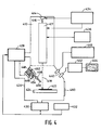
- FIG. 4 schematically shows one embodiment of a shaped focused ion beam (“FIB") system suitable for use with the present invention. Note that the identified components are not required in all applications. Moreover, the depicted sizes and relative positions are not necessarily to scale or consistent with all configurations. Also, this system can be used either for a projection approach or for an angular apertured approach depending on the particular configuration of the optical components in the FIB column.
- FIB shaped focused ion beam
- the depicted shaped beam system includes an evacuated chamber 410 having a liquid metal ion source 414 and a focusing column 417, which includes an optical system such as is shown in the block diagram of Figure 5 for defining a desired shaped ion beam 418 and focusing it onto a target work piece 422.
- Focusing column 417 uses a two-lens ion focusing structure for generating an angular apertured shaped beam.
- the lenses and other "optical" elements used with focused ion beams use electrostatic or magnetic fields to control ions in the beam, and that the optical elements are controlling a stream of ions.
- the designs may include only one or up to several lenses.
- the principles of the angular apertured approach are discussed using this FIB system, they apply equally to other charged particle systems (such as e-beam systems) as long as suitable optical components for such other systems are used.
- Unfocused ion beam 416 passes from source 414 through column 417 emitting a shaped beam 418 toward work piece 422, which is removably mounted on movable X-Y stage 424 within the lower portion of chamber 426.
- the work piece 422 can be any material that may be worked upon by beam 418 to achieve a desired result. It could comprise, for example, a semiconductor device, photo-lithographic mask, magnetic storage head, and the like. The particular shaped beam parameters being used will depend on the object material, as well as on the result that is desired.
- An ion pump 428 is employed for evacuating neck portion 410.
- the chamber 426 is evacuated with turbo-molecular and mechanical pumping system 430 under the control of vacuum controller 432.
- High voltage power supply 434 is connected to liquid metal ion source 414, as well as to appropriate electrodes in focusing column 417 for forming an approximately 30 keV ion beam 418 and directing the same downwardly.
- Controller 436 is coupled to the focusing column 417 and in particular to deflector plates, a stigmator, and to a variable axis, variable shape aperture within the focusing column 417 in order to control beam 418, for example, to rotate, deform, and/or re-position it on the target work piece 422 in accordance with a desired task.
- controller 436 Through controller 436, a user can control beam 418 to be scanned in a desired manner through commands entered into a conventional user interface (not shown). Alternatively, controller 436 may access a memory storage device to upload instructions to cause the controller to control the system to scan a path, using a predefined beam shape.
- the source 414 typically provides a metal ion beam of gallium from a field ion emission source (liquid metal ion source (LMIS)), although other ion sources, such as a multi-cusp or other plasma ion source, can be used. While this source is typically capable of being focused into a sub one-tenth micron wide beam at work piece 422, one advantage of the invention is that it doesn't always require such acuity. In fact, using a D-shaped aperture with large beam current, it is capable of achieving equivalent (or even better) sharpness with the beam focused down to a lesser degree (e.g., focused to 5 microns). This is because the beam spot has a sufficiently sharp edge resolute enough for performing a desired application.
- An electron multiplier 440 used for detecting secondary emission for imaging is connected to a power supply and controls 445 and to video circuit 442, which supplies drive for video monitor 444 for viewing work piece 422 as it is being worked upon.
- a gas source 446 is located inwardly of the side of chamber 426 by translation device 448 adapted for positioning the source via support structure within bellows 452.
- Gas source 446 includes a reservoir 454 with a heater, which may comprise a membrane type heating device and can be used for raising the temperature of a compound within reservoir 454 to a temperature for providing a suitable stream of molecules for beam-induced reactions as hereinafter more fully disclosed.
- a transfer tube or nozzle 456 comprising a capillary tube provided by a hypodermic needle extends from reservoir 454 and is connected thereto via control valve 458 adapted for releasing gaseous vapor.
- the nozzle is extended and translated in orthogonal directions substantially perpendicular to its axis employing translation apparatus 448, so that gaseous vapor can be aimed directly toward a region on the target surface of work piece 422.
- a door 460 is opened for inserting work piece 422 on stage 424 which may be heated.
- the door is interlocked so that it cannot be opened if the temperature in reservoir 454 is substantially above room temperature.
- a gate valve is closed before door 460 can be opened to seal off the ion source and focusing column apparatus.
- valve 458 may be opened by withdrawing an actuator rod from outside the apparatus to open and regulate the position of valve plunger, while the nozzle 456 is directed towards the desired area of the work piece.
- Bellows 452 accommodate movement of the nozzle assembly and reservoir relative to the work piece without affecting the vacuum within chamber 426.
- the vacuum control system along with the heater of gaseous vapor source 446 are operated to provide an appropriate vapor pressure condition for establishing a gaseous vapor flux in the chamber as directed toward substrate 422 for etching or depositing material.
- the reservoir is heated to a predetermined temperature.
- the high voltage power supply 434 provides an appropriate acceleration voltage to electrodes in ion beam column 417 for energizing and focusing ion beam 418. When it strikes the work piece having condensed gaseous vapor adhered thereupon, the ion beam provides energy for initiating a reaction between the gaseous compound and the substrate and for either enhanced etching/milling of or material deposition upon the work piece.
- the vacuum system provides a vacuum of between approximately 1x10 -7 mbar and 5x10 -4 mbar within chamber 426.
- the chamber background pressure is suitably about 1x10 -5 mbar.
- the gaseous source 446 is heated to a temperature for providing an appropriate gaseous flux via the capillary tube of the hypodermic needle, while the metal ion source and focusing column are suitably controlled for generating a corresponding appropriate ion flux. Skilled persons can readily determine appropriate pressures and gas flows for any particular application.
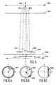
- Figure 5 is a hybrid block/ray diagram for one embodiment of a FIB column 417 of the present invention. It depicts a configuration for the basic optical components that affect beam spot shape and sharpness in connection with the angular aperture beam-shaping techniques discussed herein. Also shown are defined parameters that are used for the same.
- the column includes a particle beam axis 501, source plane 502, first lens 504, variable axis beam shaping aperture 506, second lens 508, stigmator/deflector assembly 510, and target work piece 522. Also shown is the first-order focal plane 512, along with beam shape parameters: Z o (520), being the distance from the first order focal plane to the target plane, and K Off (521), being the displacement between the beam optical axis and the beam shaping aperture axis.
- Z o 520
- K Off 521
- the depicted focusing configuration employs an angular aperture approach.
- the source is imaged to the target surface (albeit out of focus by a set amount), and the shaping aperture 506 is formed to allow only ions having particular maximum incidence angles, at the aperture's sharp edge, pass through to the target surface.
- the sharp edge of the aperture is imaged to the target plane.
- the target work piece 422 is placed a defocus distance, Zo, away from the first order focal plane.
- Z o may be positive, negative or 0.
- Z o may be positive, negative or 0.
- if positive it is move away from the focal plane toward the second lens and is said to be “under-focused.”
- Conversely if negative and thereby placed off of the focal plane away from the second lens, it is "over-focused.”
- the values of Z o , K off , and other parameters can be manipulated, as will be discussed further below, to generate various sharp-edged shaped beams having different currents and current density profiles. In the sections below, different approaches and considerations for generating desired beam spots are discussed.
- the deflector/stigmator assembly 510 for simplicity, is lumped together in this drawing, but persons of skill will recognize that this assembly encompasses two separate functions and could certainly be implemented with two separate devices.
- a conventional electrostatic dual octupole may be used for making stigmation adjustments and to deflect the shaped beams as taught herein.
- the dual octupole is shown disposed above the second lens 508, other stigmation and scan designs may be employed, such as a single octupole between the second lens and the target
- the simulations take into account optical parameters including spherical aberration, chromatic aberration, de-magnified source size, off-axis aperture displacement, maximum allowed beam incidence angle, and stigmation.
- the simulated beam densities use the X (or Y) density, dN(X)/dX, as opposed to the commonly used radial density. This is a better model for most sharp edge milling applications.
- a "low current” beam is generally defined as a beam that is mostly chromatic aberration limited, or around or smaller than 100 pA.
- a "high current” beam is a beam that is mostly spherical aberration limited, or with current that is close to or greater than 10 nA.
- beams having currents falling between these values may be deemed as low or high current beams.
- FIGS. 6A through 6C shows different methods of calculating beam densities, the different methods being useful for different beam shapes.
- FIG. 6A shows that the radial density is typically determined by considering a annular portion 601 (with a radial dimension dR) using the equation dN(R)/dR.
- FIG. 6B shows another method of determining radial density that is likely better for imaging in some cases in which the beam lacks circular symmetry.
- the density is determined by considering a portion 602, (with an angular dimension dT), of an annular ring 601 (with a radial dimension dR), and calculating density as (dN(R,T)/ R dR dT.
- FIG.6C shows a method useful calculating density for many beam shapes that useful for milling applications.
- the simulated beam density is the X (or Y) density determined for a segment 603 and calculated as dN(X)/dX.
- Monte-Carlo beam simulator which is formulated on MS Excel spreadsheets, to further explore and extend these shaped beams.
- This simulator gives considerably more information regarding beam shape and density with round, D-shaped, and rectangular apertures under various conditions. Included in the simulator are spherical aberration, chromatic aberration, demagnified source size, off-axis apertures, and stigmation.
- FIGS. 7A through 37B show scatter plots and current density plots for simulations for various angular aperture shaped beams.
- D G 0.01 ⁇ m
- the aperture generates a 1.0 mrad maximum half-angle for the beam leaving the final lens, which produces a 7.6 pA beam current assuming a source brightness of 3.1 x 10 6 A/(cm 2 ⁇ sr).
- This 1 mrad half-angle also generates spherical and chromatic radii of 0.001 ⁇ m and 0.027 ⁇ m, respectively, at the first order focal plane.
- the scatter plot of Figure 7A represents the beam shape, which is round, and the X- and Y- beam densities are shown in Figure 7B.
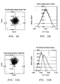
- Figures -A show the Rectangular Aperture Beam Scatter Plot
- Figure -B and -C show the Rectangular Aperture Beam Density.
- the beam becomes broader and the current density more uniform, which can be utilized for a low beam density gas chemistry application, for example.
- a disadvantage to the under-focused, aperture offset rectangular aperture beam in Figures 13A-C in some applications, however, is that it has a larger full width than the first order focused, centered aperture round beam in Figures 11A-C. This can be a disadvantage regarding slice-and-view milling applications.
- Figures -A show the Rectangular Aperture Beam Scatter Plot, while Figure -B and -C show the Rectangular Aperture Beam Density.
- the first order focused, non-aperture offset beam shown in Figure 18A-C has less width in the Y direction than the round aperture low-current beam, and it has twice the beam current.
- Under-focus and aperture offset Figures 19A-C and 20A-C
- the Y-edge sharpness of this rectangular beam is better than the offset, under-focused round aperture beam in Figures 10A and B, and its beam width is less than half.
- the beam width is now down to about the width of the first order focused, non-aperture offset round beam in Figures 7A and B.
- this rectangular beam has twice the beam current as the round beam plus it has a sharper edge (which for the round beam requires under-focused, aperture-offset conditions) and at the same time has a small beam width (which for the round beam requires first order focus and non aperture offset conditions).
- a rectangular aperture beam is ideally suited for many slice and view applications. Note that one could increase the current even more by employing a line source in a microbeam plasma source in conjunction with these rectangular aperture cases.
- Figures 21A and B to 26A and B show plots for different high current, D-shaped beam spots.
- D-shaped refers to any bisected or semi elliptical shape. It includes any substantially elliptical shape bisected along either its minor or major axis. In either case, it is left with a straight edge portion that may be a small or larger part of the ellipse's overall circumference.
- Figures -A show D-aperture Beam Scatter Plots
- figurs -B show D-aperture Beam Densities.
- Figures 21A and B demonstrates the beam under the first order focus condition.
- the beam is quite broad.
- the under-focus is increased, the beam moves from the +Y to the -Y side of the Y-axis.
- Z 0 0.27 mm
- the Y-edge sharpness is limited only by the de-magnified source size, small chromatic aberration contributions, and beam interaction effects, which are not included in the present beam simulation.
- the Y-beam density falls weakly with -Y and the X-beam density is somewhat flat. This beam can be quite useful for high current milling with a sharp edge, such as for initial material removal for integrated circuit cross sections.
- this under-focused beam is relatively large and has a lower current density, but none-the-less has this sharp, straight edge.
- the beam density in the Y-direction is somewhat tapered away from the sharp edge, and the X-density distribution is somewhat uniformly distributed.
- This beam having large beam current and a sharp edge could be useful for hogging out cross sections, where it can be scanned in X- and Y- directions in a pattern towards the desired target interface.
- the sloped density distribution in the Y-direction can be beneficial to generate a sloping hole towards the cross section target.
- Beam chemistry can perhaps be employed since the beam has relatively low density with its large area.
- An LMIS FIB column lends itself well to high current, D- aperture optics, because the two-lens magnification saturates at about 1.4, since high magnification makes the first lens spherical aberration contribution very large. One can then increase beam current using larger D- apertures and still obtain this sharp milling beam edge.
- Figures 24A to 26B demonstrate further increases in the under-focus condition.
- the beam still has a sharp Y-edge but increases in radius.
- the beam density becomes more uniform in both X- and Y- directions with increasing under-focus, which can be useful for gas chemistry.
- the scatter plots show greater beam density d 2 N/dXdY near the edges, but if the beam is scanned in the X direction, its Y-beam density dN/dY is relatively uniform in the Y-direction over the beam width.
- a 50 nA round aperture beam is shown for comparison to the D-aperture beam, where a moderate under-focus is employed to reduce the round aperture beam tails.
- Both the D- and round-aperture Y-beam densities are shown in Figure 28 for comparison, with the D-aperture beam density shown with triangles and the round-aperture beam density shown with diamonds.
- the round beam has a 15-85% rise of about 0.24 ⁇ m, which is about 3.4 times the D-aperture edge of about 0.07 ⁇ m.
- the round beam edge will be even larger, because the single sided 15-85% rise underestimates the milled edge when a gaussian-like peak is employed versus an edge, which does not fall so rapidly on the opposite side.
- the D-aperture beam full width is about 2 times larger, but for cross sectioning and other applications, where the beam is scanning to generate a relatively large hole, this is not a disadvantage.
- This beam has been under-focused to the same condition as the corresponding rectangular aperture beam, and has great similarity to the rectangular aperture beam. Note that the beam density in the Y-direction falls more rapidly than the rectangular aperture case. This shows that tuning the aperture shape can modify the beam density shape in Y.
- Other aperture shapes (such as a truncated triangle) can generate other results.
- a stigmator for aligning a beam's sharp edge with a target work piece axis (e.g., wafer device axis, stage axis) is examined.
- a chromatic aberrated (with little or no spherical aberration) rectangular aperture beam is used in confirming that one can rotate it with a stigmator and still preserve its sharp edge.
- Figure 30A-C (Round Aperture Beam Scatter Plots) demonstrate such a rectangular aperture beam using a 45 degree stigmator setting to stretch and shrink the beam angles in perpendicular, +45 degree and - 45 degree directions with reference to the X-axis.
- the chromatic limited beam having aperture offset and under-focus can be rotated small amounts without destroying the sharp edge.
- Figures 31A-C show similar simulations and results with a de-magnified source added to the beam. As seen in Figures 32A and C when spherical aberration is added to the chromatic and source contributions, the beam becomes more fuzzy, but the rotation still produces a reasonably sharp edge when the spherical contribution is moderate.
- FIG. 33D shows stigmation with greater under-focus, which doesn't significantly improve it, but slight aperture Y-offset helps slightly.
- Figures 34A to 37B spherical aberrated, rectangular aperture beams can be improved with defocus and stigmation.
- Figures -A show Rectangular Aperture Beam Scatter Plots
- figures -B show Rectangular Aperture Beam Density Plots.
- Figures 34A and B show a spherical limited rectangular beam with first order focus
- Figures 35A and B show the beam under X-axis, LCD under-focus conditions. In these simulations no chromatic aberration or de-magnified source contributions were included so that the spherical aberration behavior would be more isolated and thus better understood.
- the X- and Y- beam sizes are reduced with the spherical rays folded back over the origin, but the Y-axis rays are now too under-focused resulting in a beam that is broader than it needs to be.
- Figures 36A and B show the case with both under-focus and stigmation, where the under-focus is set to 1 ⁇ 2 the LCD under-focus value, and the stigmator amplitude is set to 1 ⁇ 4 the LCD under-focus value.
- Increasing the under-focus yields the beam of Figures 37A and B, which is a nice narrow beam in both directions and could be useful for TEM sample biopsy and other milling, including using a FIB or plasma ion beam column. It can be seen that the beam in Figures 36A and B is narrower in the Y-direction than the beam of Figures 37A and B, but its X-axis tails are more extensive.
- Table 1 summarizes the above simulations. It demonstrates that the 0.031 nA centered rectangular aperture beam at the first order focus plane has about the same edge resolution as the corresponding centered round aperture beam, and the former has 4.1 times more beam current.
- the beam edge resolution using the under-focused and offset rectangular aperture beam has about twice the edge resolution as the under-focused and offset round aperture beam.
- This rectangular aperture beam also has about the same or smaller Y-full width as the corresponding round beam, but it has about a 3.3 times larger X-full width. This large X-width makes little difference for scan milling sharp edges.
- the rectangular aperture with first order focus as well as the rectangular aperture with under (or over) focused and aperture offset are valuable for cross section cleanup, slice-and-view and other applications.
- the D-shaped aperture In the large current, spherical aberration case, the D-shaped aperture generates a D-shaped beam with a sharp, straight edge when properly under-focused.
- This D-aperture, 50 nA beam has a 3.5X sharper Y-edge than the centered round aperture beam with the same beam current.
- the D-aperture produces an initial Y-tail (towards the aperture flat Y-edge) that is smaller than the round aperture beam tail.
- D-aperture beams can be useful for hogging cross sections, and can be particularly advantageous if gas chemistry is employed.
- the chromatic limited rectangular aperture beam can be rotated using the stigmator to align the sharp edge to a tool or sample axis. This will also work for other aperture shapes having a sharp edge.
- this stigmator adjustment works less well, as the beam may tear or become distorted.
- the D-aperture could be mechanically rotated about the optical axis to align it to the target, or the target can be rotated.
- a spherical aberration limited rectangular aperture beam can be reduced in size by introducing combined under-focus and stigmation. This process can also be applied to other aperture shapes, such as the ellipse or half-ellipse.
- a spherical limited beam employed with a rectangular or elliptical aperture can be reduced in size by tuning the focus and stigmation such that the stigmation is accentuated in the long aperture (X-) direction and subdued in the Y-direction. For example, this can be accomplished by tuning the focus and stigmation approximately to Z 0 ⁇ 3/8 C S A 0X 2 and K ST ⁇ 3/16 A 0X 2 , where X corresponds to the rectangular aperture long direction and K ST is the stigmation amplitude.
Landscapes
- Chemical & Material Sciences (AREA)
- Engineering & Computer Science (AREA)
- Analytical Chemistry (AREA)
- Physics & Mathematics (AREA)
- Nanotechnology (AREA)
- Mathematical Physics (AREA)
- Theoretical Computer Science (AREA)
- Crystallography & Structural Chemistry (AREA)
- Plasma & Fusion (AREA)
- Electron Beam Exposure (AREA)
- Welding Or Cutting Using Electron Beams (AREA)
Applications Claiming Priority (2)
| Application Number | Priority Date | Filing Date | Title |
|---|---|---|---|
| US688810 | 2003-10-17 | ||
| US10/688,810 US6977386B2 (en) | 2001-01-19 | 2003-10-17 | Angular aperture shaped beam system and method |
Publications (2)
| Publication Number | Publication Date |
|---|---|
| EP1524681A2 true EP1524681A2 (fr) | 2005-04-20 |
| EP1524681A3 EP1524681A3 (fr) | 2006-06-21 |
Family
ID=34377681
Family Applications (1)
| Application Number | Title | Priority Date | Filing Date |
|---|---|---|---|
| EP04077809A Withdrawn EP1524681A3 (fr) | 2003-10-17 | 2004-10-13 | Appareil à faisceau de particules avec section variable |
Country Status (3)
| Country | Link |
|---|---|
| US (1) | US6977386B2 (fr) |
| EP (1) | EP1524681A3 (fr) |
| JP (1) | JP5048919B2 (fr) |
Cited By (1)
| Publication number | Priority date | Publication date | Assignee | Title |
|---|---|---|---|---|
| WO2024091829A1 (fr) * | 2022-10-24 | 2024-05-02 | Applied Materials Israel Ltd. | Procédé de création d'une surface diagonale lisse à l'aide d'un faisceau ionique focalisé et d'une stratégie de balayage innovante |
Families Citing this family (29)
| Publication number | Priority date | Publication date | Assignee | Title |
|---|---|---|---|---|
| JP5033314B2 (ja) * | 2004-09-29 | 2012-09-26 | 株式会社日立ハイテクノロジーズ | イオンビーム加工装置及び加工方法 |
| JP5509239B2 (ja) * | 2004-09-29 | 2014-06-04 | 株式会社日立ハイテクノロジーズ | イオンビーム加工装置及び加工方法 |
| US7755513B2 (en) * | 2006-01-13 | 2010-07-13 | Bwt Property, Inc. | Visual navigational aids based on high intensity LEDS |
| JP2007248091A (ja) * | 2006-03-14 | 2007-09-27 | Jeol Ltd | 試料作製装置及び試料作成方法 |
| JP5127148B2 (ja) * | 2006-03-16 | 2013-01-23 | 株式会社日立ハイテクノロジーズ | イオンビーム加工装置 |
| JP4781211B2 (ja) * | 2006-09-25 | 2011-09-28 | 株式会社荏原製作所 | 電子線装置及びこれを用いたパターン評価方法 |
| JP2008166137A (ja) * | 2006-12-28 | 2008-07-17 | Sii Nanotechnology Inc | 集束イオンビーム装置 |
| US8303833B2 (en) * | 2007-06-21 | 2012-11-06 | Fei Company | High resolution plasma etch |
| EP2063450A1 (fr) * | 2007-11-21 | 2009-05-27 | FEI Company | Procédé pour l'obtention d'une image de transmission de balayage d'un échantillon dans un appareil d'optique corpusculaire |
| US8168961B2 (en) * | 2008-11-26 | 2012-05-01 | Fei Company | Charged particle beam masking for laser ablation micromachining |
| WO2010140236A1 (fr) * | 2009-06-03 | 2010-12-09 | 三菱電機株式会社 | Dispositif d'irradiation par faisceau de particules |
| US8350237B2 (en) | 2010-03-31 | 2013-01-08 | Fei Company | Automated slice milling for viewing a feature |
| US8278623B2 (en) | 2011-01-14 | 2012-10-02 | Kla-Tencor Corporation | High-vacuum variable aperture mechanism and method of using same |
| US8664594B1 (en) | 2011-04-18 | 2014-03-04 | Kla-Tencor Corporation | Electron-optical system for high-speed and high-sensitivity inspections |
| US10410828B2 (en) * | 2014-12-22 | 2019-09-10 | Carl Zeiss Microscopy, Llc | Charged particle beam system and methods |
| US10535491B2 (en) | 2015-01-20 | 2020-01-14 | American Science And Engineering, Inc. | Dynamically adjustable focal spot |
| JP2017020106A (ja) | 2015-07-02 | 2017-01-26 | エフ・イ−・アイ・カンパニー | 高スループット・パターン形成のための適応ビーム電流 |
| US9679742B2 (en) * | 2015-10-30 | 2017-06-13 | Fei Company | Method for optimizing charged particle beams formed by shaped apertures |
| CN105668514B (zh) * | 2016-01-25 | 2019-04-23 | 北京航空航天大学 | 一种聚焦离子束-电子束双束融合可控微纳加工的方法 |
| US10497536B2 (en) * | 2016-09-08 | 2019-12-03 | Rockwell Collins, Inc. | Apparatus and method for correcting arrayed astigmatism in a multi-column scanning electron microscopy system |
| ES2738911A1 (es) * | 2018-07-25 | 2020-01-27 | Consejo Superior Investigacion | Procedimiento para depositar elementos sobre un sustrato de interes y dispositivo |
| US11440151B2 (en) | 2019-06-07 | 2022-09-13 | Applied Materials Israel Ltd. | Milling a multi-layered object |
| US11226230B2 (en) | 2019-07-30 | 2022-01-18 | Applied Materials Israel Ltd. | Method for noise reduction and a detection circuit |
| US10971618B2 (en) * | 2019-08-02 | 2021-04-06 | Applied Materials Israel Ltd. | Generating milled structural elements with a flat upper surface |
| US11276557B2 (en) | 2019-09-17 | 2022-03-15 | Applied Materials Israel Ltd. | Forming a vertical surface |
| JP7354037B2 (ja) | 2020-03-23 | 2023-10-02 | 株式会社日立ハイテクサイエンス | 集束イオンビーム加工装置 |
| US11694934B2 (en) * | 2021-09-21 | 2023-07-04 | Applied Materials Israel Ltd. | FIB delayering endpoint detection by monitoring sputtered materials using RGA |
| CN117293005A (zh) * | 2022-06-23 | 2023-12-26 | Fei 公司 | 聚焦离子束系统和方法 |
| JPWO2024157319A1 (fr) * | 2023-01-23 | 2024-08-02 |
Family Cites Families (58)
| Publication number | Priority date | Publication date | Assignee | Title |
|---|---|---|---|---|
| US3699334A (en) * | 1969-06-16 | 1972-10-17 | Kollsman Instr Corp | Apparatus using a beam of positive ions for controlled erosion of surfaces |
| US4389571A (en) * | 1981-04-01 | 1983-06-21 | The United States Of America As Represented By The United States Department Of Energy | Multiple sextupole system for the correction of third and higher order aberration |
| USRE33193E (en) * | 1981-09-30 | 1990-04-03 | Hitachi, Ltd. | Ion beam processing apparatus and method of correcting mask defects |
| JPS59168652A (ja) * | 1983-03-16 | 1984-09-22 | Hitachi Ltd | 素子修正方法及びその装置 |
| GB8415623D0 (en) * | 1984-06-19 | 1984-07-25 | Nixon W C | Charged particle sources |
| US4698236A (en) * | 1984-10-26 | 1987-10-06 | Ion Beam Systems, Inc. | Augmented carbonaceous substrate alteration |
| US4634871A (en) * | 1985-01-14 | 1987-01-06 | Hughes Aircraft Company | Method and apparatus for spot shaping and blanking a focused beam |
| US4661709A (en) * | 1985-06-28 | 1987-04-28 | Control Data Corporation | Modular all-electrostatic electron-optical column and assembly of said columns into an array and method of manufacture |
| US4694178A (en) * | 1985-06-28 | 1987-09-15 | Control Data Corporation | Multiple channel electron beam optical column lithography system and method of operation |
| JPS62281349A (ja) * | 1986-05-29 | 1987-12-07 | Seiko Instr & Electronics Ltd | 金属パタ−ン膜の形成方法及びその装置 |
| NL8602176A (nl) * | 1986-08-27 | 1988-03-16 | Philips Nv | Ionen bundel apparaat voor nabewerking van patronen. |
| US4724359A (en) * | 1986-10-17 | 1988-02-09 | General Electric Company | Laminar flow guns for light valves |
| AT391771B (de) * | 1987-03-05 | 1990-11-26 | Ims Ionen Mikrofab Syst | Einrichtung zur verkleinernden oder 1 : 1 ionenprojektionslithographie |
| US4874460A (en) * | 1987-11-16 | 1989-10-17 | Seiko Instruments Inc. | Method and apparatus for modifying patterned film |
| JPH01236561A (ja) * | 1987-11-28 | 1989-09-21 | Fuji Electric Co Ltd | イオンビーム装置 |
| US6048588A (en) * | 1988-07-08 | 2000-04-11 | Cauldron Limited Partnership | Method for enhancing chemisorption of material |
| EP0367496B1 (fr) * | 1988-10-31 | 1994-12-28 | Fujitsu Limited | Dispositif et méthode de lithographie par faisceau de particules chargées |
| JPH02295040A (ja) * | 1989-05-10 | 1990-12-05 | Hitachi Ltd | 集束イオンビーム装置 |
| JP2708547B2 (ja) * | 1989-05-10 | 1998-02-04 | 株式会社日立製作所 | デバイス移植方法 |
| US5093572A (en) * | 1989-11-02 | 1992-03-03 | Mitsubishi Denki Kabushiki Kaisha | Scanning electron microscope for observation of cross section and method of observing cross section employing the same |
| US4994711A (en) * | 1989-12-22 | 1991-02-19 | Hughes Aircraft Company | High brightness solid electrolyte ion source |
| NL9000822A (nl) * | 1990-04-09 | 1991-11-01 | Philips Nv | Werkwijze voor bestraling van een object met een geladen deeltjesbundel en inrichting voor uitvoering van de werkwijze. |
| US5126287A (en) * | 1990-06-07 | 1992-06-30 | Mcnc | Self-aligned electron emitter fabrication method and devices formed thereby |
| US5061850A (en) * | 1990-07-30 | 1991-10-29 | Wisconsin Alumni Research Foundation | High-repetition rate position sensitive atom probe |
| US5149974A (en) * | 1990-10-29 | 1992-09-22 | International Business Machines Corporation | Gas delivery for ion beam deposition and etching |
| US5188705A (en) * | 1991-04-15 | 1993-02-23 | Fei Company | Method of semiconductor device manufacture |
| WO1994013010A1 (fr) * | 1991-04-15 | 1994-06-09 | Fei Company | Procede de profilage d'elements de dispositifs a semi-conducteurs |
| JP2774884B2 (ja) * | 1991-08-22 | 1998-07-09 | 株式会社日立製作所 | 試料の分離方法及びこの分離方法で得た分離試料の分析方法 |
| JPH05114376A (ja) * | 1991-10-23 | 1993-05-07 | Fujitsu Ltd | 電子ビーム露光装置及び電子ビームの制御方法 |
| US5389196A (en) * | 1992-01-30 | 1995-02-14 | Massachusetts Institute Of Technology | Methods for fabricating three-dimensional micro structures |
| JP3117836B2 (ja) * | 1993-03-02 | 2000-12-18 | セイコーインスツルメンツ株式会社 | 集束イオンビーム装置 |
| US5825035A (en) * | 1993-03-10 | 1998-10-20 | Hitachi, Ltd. | Processing method and apparatus using focused ion beam generating means |
| US5504340A (en) * | 1993-03-10 | 1996-04-02 | Hitachi, Ltd. | Process method and apparatus using focused ion beam generating means |
| EP0637057B1 (fr) * | 1993-07-30 | 1996-12-11 | International Business Machines Corporation | Méthode et appareil pour déposer des lignes fine de métal sur un substrat |
| US5435850A (en) * | 1993-09-17 | 1995-07-25 | Fei Company | Gas injection system |
| US5524018A (en) * | 1993-10-04 | 1996-06-04 | Adachi; Yoshi | Superior resolution laser using bessel transform optical filter |
| US5528048A (en) * | 1994-03-15 | 1996-06-18 | Fujitsu Limited | Charged particle beam exposure system and method |
| AU2914095A (en) * | 1994-06-28 | 1996-01-25 | Fei Company | Charged particle deposition of electrically insulating films |
| JP3265901B2 (ja) * | 1995-03-24 | 2002-03-18 | 株式会社日立製作所 | 集束イオンビーム装置及び集束イオンビーム照射方法 |
| JP3263920B2 (ja) * | 1996-02-01 | 2002-03-11 | 日本電子株式会社 | 電子顕微鏡用試料作成装置および方法 |
| US5825038A (en) * | 1996-11-26 | 1998-10-20 | Eaton Corporation | Large area uniform ion beam formation |
| JPH09283496A (ja) * | 1996-04-18 | 1997-10-31 | Hitachi Ltd | 荷電粒子ビーム照射によるパターン形成方法及びその装置 |
| US5916424A (en) * | 1996-04-19 | 1999-06-29 | Micrion Corporation | Thin film magnetic recording heads and systems and methods for manufacturing the same |
| US6128134A (en) * | 1997-08-27 | 2000-10-03 | Digital Optics Corporation | Integrated beam shaper and use thereof |
| US6042738A (en) * | 1997-04-16 | 2000-03-28 | Micrion Corporation | Pattern film repair using a focused particle beam system |
| US6274877B1 (en) * | 1997-05-08 | 2001-08-14 | Canon Kabushiki Kaisha | Electron beam exposure apparatus |
| JPH1177333A (ja) * | 1997-09-09 | 1999-03-23 | Hitachi Ltd | 集束イオンビーム加工装置及びその方法 |
| JPH11154479A (ja) * | 1997-11-20 | 1999-06-08 | Hitachi Ltd | 2次電子画像検出方法及びその装置並びに集束荷電粒子ビームによる処理方法及びその装置 |
| JP2926132B1 (ja) * | 1998-01-23 | 1999-07-28 | セイコーインスツルメンツ株式会社 | 集束イオンビームによる二次イオン像観察方法 |
| US6441384B1 (en) * | 1998-04-08 | 2002-08-27 | Nikon Corporation | Charged particle beam exposure device exhibiting reduced image blur |
| US5945677A (en) * | 1998-04-10 | 1999-08-31 | The Regents Of The University Of California | Focused ion beam system |
| US6011269A (en) * | 1998-04-10 | 2000-01-04 | Etec Systems, Inc. | Shaped shadow projection for an electron beam column |
| US6277542B1 (en) * | 1998-06-05 | 2001-08-21 | Nikon Corporation | Charged-particle-beam projection-exposure methods exhibiting more uniform beam-current density |
| US6414307B1 (en) * | 1999-07-09 | 2002-07-02 | Fei Company | Method and apparatus for enhancing yield of secondary ions |
| US6635891B1 (en) * | 1999-09-22 | 2003-10-21 | Nikon Corporation | Hollow-beam apertures for charged-particle-beam microlithography apparatus and methods for making and using same |
| EP1210723B1 (fr) * | 2000-01-21 | 2009-03-18 | Fei Company | Faisceaux ioniques focalises modeles et a faible densite |
| US6727500B1 (en) * | 2000-02-25 | 2004-04-27 | Fei Company | System for imaging a cross-section of a substrate |
| JP3597761B2 (ja) * | 2000-07-18 | 2004-12-08 | 株式会社日立製作所 | イオンビーム装置及び試料加工方法 |
-
2003
- 2003-10-17 US US10/688,810 patent/US6977386B2/en not_active Expired - Lifetime
-
2004
- 2004-10-13 EP EP04077809A patent/EP1524681A3/fr not_active Withdrawn
- 2004-10-14 JP JP2004300820A patent/JP5048919B2/ja not_active Expired - Lifetime
Non-Patent Citations (1)
| Title |
|---|
| None * |
Cited By (1)
| Publication number | Priority date | Publication date | Assignee | Title |
|---|---|---|---|---|
| WO2024091829A1 (fr) * | 2022-10-24 | 2024-05-02 | Applied Materials Israel Ltd. | Procédé de création d'une surface diagonale lisse à l'aide d'un faisceau ionique focalisé et d'une stratégie de balayage innovante |
Also Published As
| Publication number | Publication date |
|---|---|
| EP1524681A3 (fr) | 2006-06-21 |
| JP5048919B2 (ja) | 2012-10-17 |
| JP2005123196A (ja) | 2005-05-12 |
| US20040140438A1 (en) | 2004-07-22 |
| US6977386B2 (en) | 2005-12-20 |
Similar Documents
| Publication | Publication Date | Title |
|---|---|---|
| US6977386B2 (en) | Angular aperture shaped beam system and method | |
| US6949756B2 (en) | Shaped and low density focused ion beams | |
| US20240170248A1 (en) | Particle beam system | |
| IL237738A (en) | Install a bi-lens electron beam device and high resolution imaging methods with high and low beam currents | |
| US8101911B2 (en) | Method and device for improved alignment of a high brightness charged particle gun | |
| WO2007041444A2 (fr) | Colonne de faisceau d'electrons pour l'inscription de faisceaux d'electrons formes | |
| JP7554542B2 (ja) | 集束イオンビーム装置 | |
| EP3166127B1 (fr) | Système et procédé pour optimiser des faisceaux de particules chargées formés par des ouvertures de forme particulière | |
| US12505975B2 (en) | Focused ion beam system and method | |
| US5994708A (en) | Demagnifying charged-particle lithography apparatus | |
| US20240242924A1 (en) | Focused ion beam system | |
| CN113436952B (zh) | 会聚离子束加工装置 | |
| US20250285827A1 (en) | Charged particle beam device | |
| EP2182543B1 (fr) | Procédé et dispositif pour améliorer l'alignement d'un cannon à particules chargé à haute luminosité | |
| JP2024080618A (ja) | 電子ビーム装置の調整方法、装置及びプログラム |
Legal Events
| Date | Code | Title | Description |
|---|---|---|---|
| PUAI | Public reference made under article 153(3) epc to a published international application that has entered the european phase |
Free format text: ORIGINAL CODE: 0009012 |
|
| 17P | Request for examination filed |
Effective date: 20041013 |
|
| AK | Designated contracting states |
Kind code of ref document: A2 Designated state(s): AT BE BG CH CY CZ DE DK EE ES FI FR GB GR HU IE IT LI LU MC NL PL PT RO SE SI SK TR |
|
| AX | Request for extension of the european patent |
Extension state: AL HR LT LV MK |
|
| PUAL | Search report despatched |
Free format text: ORIGINAL CODE: 0009013 |
|
| AK | Designated contracting states |
Kind code of ref document: A3 Designated state(s): AT BE BG CH CY CZ DE DK EE ES FI FR GB GR HU IE IT LI LU MC NL PL PT RO SE SI SK TR |
|
| AX | Request for extension of the european patent |
Extension state: AL HR LT LV MK |
|
| AKX | Designation fees paid |
Designated state(s): DE FR GB |
|
| 17Q | First examination report despatched |
Effective date: 20070208 |
|
| STAA | Information on the status of an ep patent application or granted ep patent |
Free format text: STATUS: THE APPLICATION IS DEEMED TO BE WITHDRAWN |
|
| 18D | Application deemed to be withdrawn |
Effective date: 20070619 |