EP1524700A1 - Schalter mit einer isolierten Steuerung - Google Patents
Schalter mit einer isolierten Steuerung Download PDFInfo
- Publication number
- EP1524700A1 EP1524700A1 EP04105043A EP04105043A EP1524700A1 EP 1524700 A1 EP1524700 A1 EP 1524700A1 EP 04105043 A EP04105043 A EP 04105043A EP 04105043 A EP04105043 A EP 04105043A EP 1524700 A1 EP1524700 A1 EP 1524700A1
- Authority
- EP
- European Patent Office
- Prior art keywords
- main
- type
- area
- trigger
- terminal
- Prior art date
- Legal status (The legal status is an assumption and is not a legal conclusion. Google has not performed a legal analysis and makes no representation as to the accuracy of the status listed.)
- Granted
Links
Images


Classifications
-
- H—ELECTRICITY
- H10—SEMICONDUCTOR DEVICES; ELECTRIC SOLID-STATE DEVICES NOT OTHERWISE PROVIDED FOR
- H10D—INORGANIC ELECTRIC SEMICONDUCTOR DEVICES
- H10D64/00—Electrodes of devices having potential barriers
- H10D64/20—Electrodes characterised by their shapes, relative sizes or dispositions
- H10D64/27—Electrodes not carrying the current to be rectified, amplified, oscillated or switched, e.g. gates
- H10D64/291—Gate electrodes for thyristors
-
- H—ELECTRICITY
- H03—ELECTRONIC CIRCUITRY
- H03K—PULSE TECHNIQUE
- H03K17/00—Electronic switching or gating, i.e. not by contact-making and –breaking
- H03K17/51—Electronic switching or gating, i.e. not by contact-making and –breaking characterised by the components used
- H03K17/56—Electronic switching or gating, i.e. not by contact-making and –breaking characterised by the components used by the use, as active elements, of semiconductor devices
- H03K17/72—Electronic switching or gating, i.e. not by contact-making and –breaking characterised by the components used by the use, as active elements, of semiconductor devices having more than two PN junctions; having more than three electrodes; having more than one electrode connected to the same conductivity region
- H03K17/722—Electronic switching or gating, i.e. not by contact-making and –breaking characterised by the components used by the use, as active elements, of semiconductor devices having more than two PN junctions; having more than three electrodes; having more than one electrode connected to the same conductivity region with galvanic isolation between the control circuit and the output circuit
-
- H—ELECTRICITY
- H10—SEMICONDUCTOR DEVICES; ELECTRIC SOLID-STATE DEVICES NOT OTHERWISE PROVIDED FOR
- H10D—INORGANIC ELECTRIC SEMICONDUCTOR DEVICES
- H10D64/00—Electrodes of devices having potential barriers
- H10D64/20—Electrodes characterised by their shapes, relative sizes or dispositions
- H10D64/23—Electrodes carrying the current to be rectified, amplified, oscillated or switched, e.g. sources, drains, anodes or cathodes
- H10D64/233—Cathode or anode electrodes for thyristors
-
- H—ELECTRICITY
- H10—SEMICONDUCTOR DEVICES; ELECTRIC SOLID-STATE DEVICES NOT OTHERWISE PROVIDED FOR
- H10D—INORGANIC ELECTRIC SEMICONDUCTOR DEVICES
- H10D84/00—Integrated devices formed in or on semiconductor substrates that comprise only semiconducting layers, e.g. on Si wafers or on GaAs-on-Si wafers
- H10D84/101—Integrated devices comprising main components and built-in components, e.g. IGBT having built-in freewheel diode
- H10D84/131—Thyristors having built-in components
- H10D84/133—Thyristors having built-in components the built-in components being capacitors or resistors
Definitions
- the present invention relates generally to SCR type switches.
- SCR type switches components such as thyristors, triacs and bidirectional controlled switches of various types and comprising at least four semiconductor layers of alternate doping.
- the present invention relates more particularly the galvanic isolation of a control circuit of a switch SCR type.
- Galvanic isolation between a control circuit and one or more SCR type switches controlled is so general process using a transformer or opto-coupler. These two means of isolation are generally expensive and difficult to integrate.
- An object of the present invention is to provide a monolithic SCR type switch such as the circuit of switch control is galvanically isolated from the circuit of power of the switch.
- Another object of the present invention is to provide such a simple structure switch.
- the present invention provides to use a SCR type switch controlled in high frequency HF and integrate capacitors into the structure.
- the present invention provides a vertical SCR switch to be controlled by a high frequency signal, comprising at least four layers main types of alternate doping types through which a strong current is likely to go from one face to another between two main terminals, and including a terminal trigger connected to a trigger zone via a capacitor.
- This switch further comprises a terminal of trigger reference connected via a capacitor integrated into a trigger reference area arranged on the same face of the component as the trigger area.
- the switch is of thyristor type, comprising on the side of the front face a main semiconductor zone of a first type of doping formed in a semiconductor trigger zone of a second type of doping, a first portion of the area principal being connected to one of the main terminals, a second portion of the main zone being connected to one of the control terminals via a first capacitor integrated, and a portion of the trigger area being connected to the other control terminals through a second integrated capacitor.
- the first and second portions of the main area are two semiconducting regions disjointed.
- the second portion of the main area and the said portion of the trigger area are covered with an insulating layer and a metallization, the stacks of a semiconductor portion, an insulating layer and a metallization constituting said first and second capacitors.
- the second portion of the main area and the said portion of the Trigger area are each covered with a metallization in contact with an electrode of an integrated capacitor the other electrode is in contact with a metallization connected to a main terminal or a control terminal.
- the main area is a cathode area, the main area comprising one or more N-type semiconductor regions formed in a P-type well constituting the gate area, the P-type well being formed above a semiconductor layer of N type under which is placed a semiconductor region of type P corresponding to the anode of the thyristor.
- the second portion of the main zone corresponding to a N-type region is placed between said first portion of the main zone corresponding to an N-type region and the portion of the P-type well connected to the gate terminal.
- the first portion of the main area includes several holes corresponding to portions of the P type casing, a metallization connected to a main terminal covering the first portion of the main area and all of these holes.
- the switch is of triac type, comprising on the side of the face before a main semiconductor zone of a first type of doping formed in a box of a second type of doping, the main zone and the caisson being connected to a terminal main, a trigger region of the first type of doping being formed in the box and being connected to a control terminal through a first integrated capacitor, and a portion of the box being connected to a reference terminal of trigger via a second integrated capacitor.
- the switch is of bidirectional type, comprising on the side of the front face a semiconductor prime area of a first type of doping formed in a box of a second type of doping, the main zone and the caisson being connected to a main terminal, the whole being surrounded by a wall of isolation, a trigger region of the first type of doping being formed in the isolation wall or in a lateral extension of it and being connected to a control terminal by via a first integrated capacitor, and a portion of the box being connected to a reference terminal of trigger via a second integrated capacitor.
- Figures 2 to 6 and 8 to 11 are partial views, schematic and simplified and are only intended for simplify the understanding of the description below. The man of art will know how to make practical arrangements using known techniques. Moreover, as is usual in the domain of the representation of semiconductor components, the dimensions of the various layers and regions are not plotted at the scale.
- FIG. 1 is a diagram of a control circuit 1 of a thyristor 2 inserted into a power circuit 3.
- the power circuit 3 is shown schematically by a voltage generator V1 and a load Z1 in series between the anode and the cathode of the thyristor 2.
- the control circuit 1 is for applying a current between the trigger and the cathode of the thyristor and essentially comprises in series a generator of high frequency sinusoidal RF, a resistance of current limiting Rlim, a capacitor Cg, and a switch Sw.
- Such a circuit (without the capacitor Ck) is described in the unpublished French patent application number 0215322 of the plaintiff filed on December 4, 2002 (B5748).
- the capacitor Cg behaves like a short circuit and the variations of voltage and current are fully transmitted to the thyristor.
- This patent application states that, even if the energy supplied by the control circuit during each period is less than the energy needed to trigger the thyristor, it triggers, surprisingly, after a certain number of periods.
- FIG. 2 is a sectional view of an embodiment of a thyristor integrating the capacitor Cg as described in the aforementioned patent application.
- the thyristor includes an N-type cathode region 20 formed in a box 21 of type P, itself formed in a weakly doped substrate 22 of type N, and anode region 23 of type P on the side of the face back of the thyristor.
- the substrate 22 is surrounded by an isolation wall
- the P type box 21 corresponds to a trigger area.
- the front of the thyristor is covered an insulating layer 25 in which are provided several openings including two openings Ok and Og respectively above of the cathode region 20 and above a portion of the P-type box 21.
- a cathode metallization MK connected to a cathode terminal K is in contact with the cathode region 20 in the opening Ok.
- the back side of the component is coated of an anode metallization MA connected to an anode terminal A.
- insulating layer 26 is placed in the opening Og so as to cover a portion of the box 21.
- the insulating layer 26 is covered with a trigger metallization Mg connected to a terminal
- the trigger zone of the thyristor is thus accessible via a capacitor whose dielectric is the insulating layer 26, the electrodes corresponding to the metallization Mg and the box P 21.
- the capacitor Cg is not necessarily disposed over the region of cathode trigger.
- a planar thyristor such as that represented in FIG. 2 commonly comprises on the side of its front face an annular zone of heavily doped N type 27, called channel stop, preferably covered with a metallization 28 placed in an opening of the insulating layer 25.
- an N-type region heavily doped 29 is commonly formed in a box 30 of strongly doped type P placed on the surface of the isolation wall. box 30 is covered with a metallization 31 placed in a opening of the insulating layer 25.
- the cathode of the thyristor 2 is connected to a terminal of the power circuit which serves as reference to the control circuit.
- the control circuit has an independent reference voltage of the power circuit, isolation must be provided between the two circuits.
- the present invention proposes, in the case of a high frequency control, to ensure this isolation by inserting a capacitor Ck shown in dashed lines in FIG. the reference voltages of the control circuits and power.
- a control circuit producing a high frequency control signal and isolation capacitors on the trigger and the cathode of thyristor 2 allows to to achieve in a simple way a galvanic isolation between the circuit control and the thyristor.
- the present invention further provides a structure thyristor integrating the capacitors Cg and Ck.
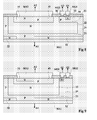
- FIG. 3 is a sectional view of an embodiment of a thyristor according to the present invention integrating the capacitors Cg and Ck.
- the assembly of the semiconductor zones and metallizations of the thyristor is similar to that of the thyristor shown in Figure 2. Similar elements are designated by the same references and will not be described in new.
- the essential difference is that a second opening Ok2 distinct from the opening Ok is formed in the insulating layer 25 above the cathode region 20.
- the aperture Ok2 has a much smaller area than that of the opening Ok and is formed near the Og opening.
- MK metallization connected to a cathode terminal K is placed in the opening Ok and constitutes as before the cathode of the circuit of power of the thyristor.
- An insulating layer 35 placed in opening Ok2 covers a small portion of the region of cathode 20.
- a metallization MK2 connected to a cathode terminal auxiliary K2 covers the insulating layer 35.
- the thyristor therefore includes two cathode terminals.
- the first terminal or terminal main K is in contact with the cathode region and is the cathode of the power circuit of the thyristor.
- the second terminal or auxiliary terminal K2 is connected to the region of cathode via a capacitor Ck whose dielectric is the insulating layer 35.
- the auxiliary terminal K2 constitutes a gate reference terminal.
- the application of a high frequency signal between trigger terminal G and the terminal Trigger reference K2 allows to activate the thyristor.
- the high frequency signal generator is isolated from the active part of the thyristor thanks to insulating layers 26 and 35.
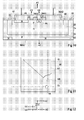
- FIG. 4 is an example of a top view of the thyristor of Figure 3 without the metallizations.
- the peripheries of box P 21 and the layer N 22 are substantially rectangular but could be circular or any other form.
- the N region 20 has a rectangle shape that lacks a corner.
- the opening Og represented by a circle is placed in the corner "missing" from area N 20 above box 21.
- Opening Ok2 has a banana shape around the missing corner at near the opening Og.
- the opening Ok discovers the majority from the region N 20 not discovered by the opening Ok2.
- the view in section of Figure 3 is carried out at the plane AA 'shown in figure 4.
- FIG. 5 is a sectional view of a thyristor according to an alternative embodiment of the present invention.
- the thyristor represented is identical to that of Figure 3 except that the N-type cathode region 20 formed in the P well 21 is replaced by two regions N 40 and 41.
- Region N 40 is formed under the Ok opening and the N region 41 is formed under Ok2 opening.
- the region N 40 preferably comprises holes transmitter short circuit corresponding to portions 42 to 46 of the box P 21.
- FIG. 6 is an example of a top view of the thyristor of Figure 5. This view from above is substantially identical to that of Figure 4 except that the cathode region N 20 is replaced by two regions N 40 and 41.
- the sectional view of the Figure 5 is made at the plane BB 'of Figure 6.
- An advantage of the embodiment of FIGS. 5 and 6 is that it optimizes both the trigger sensitivity of the thyristor and its reversal characteristics in dV / dt (reversal caused by a sudden change in voltage between the main terminals).
- the region N 41, the box P 21, the layer N 22 and region 23 constitute a very "auxiliary" thyristor sensitive because the cathode region N 41 is placed close to trigger opening Og and no short circuit hole is provided in this cathode region.
- the region N 40, the box P 21, the layer N 22 and the region 23 constitute a main thyristor whose holding in dV / dt is good thanks to the presence of transmitter holes. The triggering of this main thyristor is caused by turning on the conduction auxiliary thyristor.
- FIG. 7 is a schematic representation of a thyristor according to the present invention.
- Trigger terminal G allows access to the trigger area via a capacitor.
- a main cathode terminal K allows to directly access the cathode zone of the thyristor.
- a auxiliary cathode terminal K2, or reference terminal of trigger, allows access to the thyristor cathode area by via a capacitor. Terminal A allows for it has direct access to the anode zone of the thyristor.
- FIG 8 is a sectional view of a switch bidirectional control according to an embodiment of the present invention.
- This bidirectional switch is constituted from a lightly doped N-type substrate 22 comprising on the side of its back side a layer 23 of type P and surrounded by a P type wall 24.
- a box 50 of type P On the front side is exposed a box 50 of type P in which is formed a region 51 of type N, constituting the two main front-facing areas of the switch.
- a region 52 of type N is formed everywhere except with respect to the region 51 of type N. thus finds two thyristor-type components in antiparallel respectively consisting of regions 51-50-22-23 and 50-22-23-52.
- the trigger zone is formed in an extension 53 towards the interior of the isolation wall 24.
- an N-type region 54 In this extension 53 is formed an N-type region 54. Above the region of type N 54 is formed a metallization MG1 connected to a terminal of trigger G1 and above a portion of region 53 is formed a metallization MG2 connected to a gate terminal G2. The MG1 and MG2 metallizations are isolated from the regions underlying semiconductors by insulating layers 55 and 56. Such a component is triggered when a high voltage frequency is applied between terminals G1 and G2.
- FIG. 9 is a sectional view constituting a variant of the bidirectional controlled switch of FIG.
- the regions related to terminals G1 and G2 are formed in an extension to inside the isolation wall 24, they are formed directly in an upper part of this isolation wall.
- FIG. 10 represents an embodiment of a triac according to the present invention.
- This triac is made up of from a weakly doped substrate type N 22 whose face rear is coated with a layer 23 of type P and is surrounded of a P-type isolation wall. 24.
- this wall of isolation may constitute the component limit or may be a boundary between this component and another component formed in the same substrate.
- a box 60 of type P is formed of side of the front face in which is formed a main region 61 of type N.
- a N-type layer 62 is formed substantially everywhere except look at the N-type region 61 on the side of the upper face.
- a metallization MA1 connected to a main terminal A1 takes the backside and MA2 metallization, in contact with the region 61 and the box 60 is formed in an opening of a layer insulating 65, this opening being designated by the reference A2 in Figure 11.
- a trigger region is formed above a portion of the box 60. This region is represented as being central in the sectional view of Figure 10 and as being lateral in the top view of Figure 11.
- the region triggering includes an N-type region 66 above which is formed a metallization MG2, with interposition an insulating layer 67 so as to form a capacitor between MG2 metallization and region 66.
- MG1 metallization is formed over a portion of the box 60 with the interposition of an insulating region 68.
- the corresponding openings are designated by the dashed regions G1 and G2.
- Figure 12 is an equivalent circuit diagram.
- the switches bidirectional illustrated in FIGS. 8 to 11 can be triggered whatever the polarity of the applied voltage between the main terminals A1 and A2.
- the present invention applies to any type of SCR type switch comprising at least four semiconductor layers of alternate doping types across which a strong current is likely to pass from one side to another between two main terminals and including a Trigger terminal connected to a trigger area.
- a switch according to the present invention further comprises a reference terminal gate trigger connected to a trigger reference area.
- Each of the trigger and trigger reference terminals is linked to a respective area of the switch via of an integrated capacitor.
- the switch can be activated by application of a high frequency signal between the terminals of trigger and trigger reference.
- the control circuit is not connected for the continuous to a circuit terminal power. This has the advantage that it is always possible, if desired, to connect the back of the grounded component, which simplifies a radiator mounting.
- the zones of a switch can be connected to terminals via a capacitor formed above the switch.
- Capacitors can by example be made between two metal electrodes, one electrodes being connected to an area of the switch by a conductor contact, the other electrode being connected to a switch terminal by another contact.
Landscapes
- Thyristors (AREA)
Applications Claiming Priority (2)
| Application Number | Priority Date | Filing Date | Title |
|---|---|---|---|
| FR0350702A FR2861229A1 (fr) | 2003-10-17 | 2003-10-17 | Commutateur scr a commande hf isole |
| FR0350702 | 2003-10-17 |
Publications (2)
| Publication Number | Publication Date |
|---|---|
| EP1524700A1 true EP1524700A1 (de) | 2005-04-20 |
| EP1524700B1 EP1524700B1 (de) | 2011-12-28 |
Family
ID=34355526
Family Applications (1)
| Application Number | Title | Priority Date | Filing Date |
|---|---|---|---|
| EP04105043A Expired - Lifetime EP1524700B1 (de) | 2003-10-17 | 2004-10-14 | Schalter mit einer isolierten Steuerung |
Country Status (3)
| Country | Link |
|---|---|
| US (1) | US7259407B2 (de) |
| EP (1) | EP1524700B1 (de) |
| FR (1) | FR2861229A1 (de) |
Cited By (1)
| Publication number | Priority date | Publication date | Assignee | Title |
|---|---|---|---|---|
| FR2918817A1 (fr) * | 2007-07-12 | 2009-01-16 | St Microelectronics Sa | Circuit de commande d'un commutateur alternatif. |
Families Citing this family (10)
| Publication number | Priority date | Publication date | Assignee | Title |
|---|---|---|---|---|
| FR2895600A1 (fr) * | 2005-12-26 | 2007-06-29 | St Microelectronics Sa | Commutateur bidirectionnel a commande hf |
| US9184097B2 (en) * | 2009-03-12 | 2015-11-10 | System General Corporation | Semiconductor devices and formation methods thereof |
| CN104347686A (zh) * | 2013-07-30 | 2015-02-11 | 安徽省祁门县黄山电器有限责任公司 | 一种高电流上升率的晶闸管芯片 |
| US9455253B2 (en) * | 2014-07-23 | 2016-09-27 | Stmicroelectronics (Tours) Sas | Bidirectional switch |
| DE102016204699B4 (de) | 2015-04-13 | 2020-07-30 | Infineon Technologies Ag | Schutzvorrichtungen mit Trigger-Vorrichtungen und Verfahren zu deren Bildung |
| US10741548B2 (en) * | 2015-04-13 | 2020-08-11 | Infineon Technologies Ag | Protection devices with trigger devices and methods of formation thereof |
| WO2018167871A1 (ja) * | 2017-03-15 | 2018-09-20 | 新電元工業株式会社 | 半導体装置 |
| FR3072520B1 (fr) | 2017-10-16 | 2020-09-04 | St Microelectronics Tours Sas | Circuit de commande d'un thyristor ou triac |
| CN109802667A (zh) * | 2019-03-08 | 2019-05-24 | 天津市津耐电器有限公司 | 一种智能无线开关驱动电路 |
| CN113410296B (zh) * | 2021-06-17 | 2024-03-22 | 吉林华微电子股份有限公司 | 可控硅结构 |
Citations (3)
| Publication number | Priority date | Publication date | Assignee | Title |
|---|---|---|---|---|
| EP0064349A1 (de) * | 1981-04-16 | 1982-11-10 | Square D Company | Festkörper-Einrichtung zur Lichtbogenunterdrückung |
| US4760432A (en) * | 1985-11-04 | 1988-07-26 | Siemens Aktiengesellschaft | Thyristor having controllable emitter-base shorts |
| EP0312088A2 (de) * | 1987-10-16 | 1989-04-19 | Kabushiki Kaisha Toshiba | Empfindlicher Thyristor mit verbesserter Rausch-Festigkeit |
Family Cites Families (3)
| Publication number | Priority date | Publication date | Assignee | Title |
|---|---|---|---|---|
| JPS5846678A (ja) * | 1981-09-14 | 1983-03-18 | Oki Electric Ind Co Ltd | Pnpn半導体スイツチ |
| CN1065992C (zh) * | 1996-08-02 | 2001-05-16 | 欧姆龙公司 | 负载控制装置 |
| US6326648B1 (en) * | 1999-12-20 | 2001-12-04 | Stmicroelectronics S.A. | Power switch with a controlled DI/DT |
-
2003
- 2003-10-17 FR FR0350702A patent/FR2861229A1/fr not_active Withdrawn
-
2004
- 2004-10-12 US US10/963,383 patent/US7259407B2/en not_active Expired - Lifetime
- 2004-10-14 EP EP04105043A patent/EP1524700B1/de not_active Expired - Lifetime
Patent Citations (3)
| Publication number | Priority date | Publication date | Assignee | Title |
|---|---|---|---|---|
| EP0064349A1 (de) * | 1981-04-16 | 1982-11-10 | Square D Company | Festkörper-Einrichtung zur Lichtbogenunterdrückung |
| US4760432A (en) * | 1985-11-04 | 1988-07-26 | Siemens Aktiengesellschaft | Thyristor having controllable emitter-base shorts |
| EP0312088A2 (de) * | 1987-10-16 | 1989-04-19 | Kabushiki Kaisha Toshiba | Empfindlicher Thyristor mit verbesserter Rausch-Festigkeit |
Cited By (1)
| Publication number | Priority date | Publication date | Assignee | Title |
|---|---|---|---|---|
| FR2918817A1 (fr) * | 2007-07-12 | 2009-01-16 | St Microelectronics Sa | Circuit de commande d'un commutateur alternatif. |
Also Published As
| Publication number | Publication date |
|---|---|
| US20050082565A1 (en) | 2005-04-21 |
| FR2861229A1 (fr) | 2005-04-22 |
| EP1524700B1 (de) | 2011-12-28 |
| US7259407B2 (en) | 2007-08-21 |
Similar Documents
| Publication | Publication Date | Title |
|---|---|---|
| EP1524700B1 (de) | Schalter mit einer isolierten Steuerung | |
| FR2750536A1 (fr) | Reseau de triacs a gachettes referencees par rapport a une electrode commune de face opposee | |
| EP1362376B1 (de) | Bistabiler elektronischer zweirichtungsschalter mit impulssteuerung | |
| FR2717308A1 (fr) | Dispositif de protection contre des surtensions dans des circuits intégrés. | |
| FR2712428A1 (fr) | Commutateur bidirectionnel à commande en tension. | |
| EP1672699A1 (de) | Spannungsgesteuerter Zweirichtungsschalter | |
| EP0599739B1 (de) | Thyristor und Aufbau von Thyristoren mit gemeinsamer Katode | |
| EP1076366A1 (de) | Zweirichtungsschalter mit verbesserten Schaltleistungen | |
| EP0793336A1 (de) | Aus-Ein-Regelung für einen Zweirichtungsmotor | |
| EP0930711A1 (de) | Zweirichtungsthyristor | |
| FR2797524A1 (fr) | Commutateur statique bidirectionnel sensible | |
| FR2960342A1 (fr) | Commutateur bidirectionnel a commande hf | |
| EP0865671B1 (de) | Normal leitender dual-thyristor | |
| EP1324394A1 (de) | Statischer bidirektionaler Schalter sensitiv in den Quadranten Q4 und Q1 | |
| EP0619637B1 (de) | Schutz eines Kraftfahrzeugdrehstromgenerators | |
| WO2002050916A1 (fr) | Commutateur statique bidirectionnel sensible | |
| EP0577531B1 (de) | Schutzdiode für ein vertikales Halbleiterbauelement | |
| EP0704903A1 (de) | Halbleitervorrichtung zur Speisung, Rückleitung und Entmagnetisierung einer induktiven Last | |
| EP1524767A2 (de) | Thyristorstruktur mit HF-Ansteuerung | |
| EP1427107B1 (de) | HF-gesteuerter Schalter des SCR-Typs | |
| EP1459388A1 (de) | Spannungsgesteuerter zweirichtungsschalter | |
| FR2590750A1 (fr) | Dispositif de commutation de puissance a semi-conducteurs et son utilisation a la realisation d'un relais statique en courant alternatif | |
| EP0302789B1 (de) | In vertikaler Integrationstechnologie hergestellter integrierter monolitischer Regulator des Induktionsanregungsstromes eines Wechselstromgenerators mittels einer Wiederdurchflussdiode | |
| EP1005159A1 (de) | Schaltkreis | |
| FR2849536A1 (fr) | Circuit d'interface de fourniture de tension |
Legal Events
| Date | Code | Title | Description |
|---|---|---|---|
| PUAI | Public reference made under article 153(3) epc to a published international application that has entered the european phase |
Free format text: ORIGINAL CODE: 0009012 |
|
| AK | Designated contracting states |
Kind code of ref document: A1 Designated state(s): AT BE BG CH CY CZ DE DK EE ES FI FR GB GR HU IE IT LI LU MC NL PL PT RO SE SI SK TR |
|
| AX | Request for extension of the european patent |
Extension state: AL HR LT LV MK |
|
| RIN1 | Information on inventor provided before grant (corrected) |
Inventor name: MAURIAC, CHRISTOPHE Inventor name: MENARD, SAMUEL |
|
| AKX | Designation fees paid | ||
| REG | Reference to a national code |
Ref country code: DE Ref legal event code: 8566 |
|
| 17P | Request for examination filed |
Effective date: 20051206 |
|
| RBV | Designated contracting states (corrected) |
Designated state(s): DE FR GB IT |
|
| R17P | Request for examination filed (corrected) |
Effective date: 20051019 |
|
| 17Q | First examination report despatched |
Effective date: 20051206 |
|
| GRAP | Despatch of communication of intention to grant a patent |
Free format text: ORIGINAL CODE: EPIDOSNIGR1 |
|
| GRAS | Grant fee paid |
Free format text: ORIGINAL CODE: EPIDOSNIGR3 |
|
| GRAA | (expected) grant |
Free format text: ORIGINAL CODE: 0009210 |
|
| AK | Designated contracting states |
Kind code of ref document: B1 Designated state(s): DE FR GB IT |
|
| REG | Reference to a national code |
Ref country code: GB Ref legal event code: FG4D Free format text: NOT ENGLISH |
|
| REG | Reference to a national code |
Ref country code: DE Ref legal event code: R096 Ref document number: 602004035846 Country of ref document: DE Effective date: 20120308 |
|
| PLBE | No opposition filed within time limit |
Free format text: ORIGINAL CODE: 0009261 |
|
| STAA | Information on the status of an ep patent application or granted ep patent |
Free format text: STATUS: NO OPPOSITION FILED WITHIN TIME LIMIT |
|
| PG25 | Lapsed in a contracting state [announced via postgrant information from national office to epo] |
Ref country code: IT Free format text: LAPSE BECAUSE OF FAILURE TO SUBMIT A TRANSLATION OF THE DESCRIPTION OR TO PAY THE FEE WITHIN THE PRESCRIBED TIME-LIMIT Effective date: 20111228 |
|
| 26N | No opposition filed |
Effective date: 20121001 |
|
| REG | Reference to a national code |
Ref country code: DE Ref legal event code: R097 Ref document number: 602004035846 Country of ref document: DE Effective date: 20121001 |
|
| GBPC | Gb: european patent ceased through non-payment of renewal fee |
Effective date: 20121014 |
|
| REG | Reference to a national code |
Ref country code: FR Ref legal event code: ST Effective date: 20130628 |
|
| PG25 | Lapsed in a contracting state [announced via postgrant information from national office to epo] |
Ref country code: DE Free format text: LAPSE BECAUSE OF NON-PAYMENT OF DUE FEES Effective date: 20130501 Ref country code: GB Free format text: LAPSE BECAUSE OF NON-PAYMENT OF DUE FEES Effective date: 20121014 |
|
| REG | Reference to a national code |
Ref country code: DE Ref legal event code: R119 Ref document number: 602004035846 Country of ref document: DE Effective date: 20130501 |
|
| PG25 | Lapsed in a contracting state [announced via postgrant information from national office to epo] |
Ref country code: FR Free format text: LAPSE BECAUSE OF NON-PAYMENT OF DUE FEES Effective date: 20121031 |