EP1524703A2 - Procédé de fabrication d'une cellule solaire à base de Si - Google Patents
Procédé de fabrication d'une cellule solaire à base de Si Download PDFInfo
- Publication number
- EP1524703A2 EP1524703A2 EP04023803A EP04023803A EP1524703A2 EP 1524703 A2 EP1524703 A2 EP 1524703A2 EP 04023803 A EP04023803 A EP 04023803A EP 04023803 A EP04023803 A EP 04023803A EP 1524703 A2 EP1524703 A2 EP 1524703A2
- Authority
- EP
- European Patent Office
- Prior art keywords
- photoelectric conversion
- silicon
- conversion device
- type
- semiconductor layer
- Prior art date
- Legal status (The legal status is an assumption and is not a legal conclusion. Google has not performed a legal analysis and makes no representation as to the accuracy of the status listed.)
- Granted
Links
- 238000006243 chemical reaction Methods 0.000 title claims abstract description 147
- XUIMIQQOPSSXEZ-UHFFFAOYSA-N Silicon Chemical compound [Si] XUIMIQQOPSSXEZ-UHFFFAOYSA-N 0.000 title claims abstract description 56
- 229910052710 silicon Inorganic materials 0.000 title claims abstract description 56
- 239000010703 silicon Substances 0.000 title claims abstract description 56
- 238000004519 manufacturing process Methods 0.000 title claims abstract description 55
- 239000010408 film Substances 0.000 claims abstract description 107
- 238000000151 deposition Methods 0.000 claims abstract description 103
- 230000008021 deposition Effects 0.000 claims abstract description 72
- 239000004065 semiconductor Substances 0.000 claims abstract description 71
- 239000000758 substrate Substances 0.000 claims abstract description 54
- 239000010409 thin film Substances 0.000 claims abstract description 52
- 239000012535 impurity Substances 0.000 claims abstract description 42
- 229910021424 microcrystalline silicon Inorganic materials 0.000 claims abstract description 38
- 238000005268 plasma chemical vapour deposition Methods 0.000 claims abstract description 21
- 239000007789 gas Substances 0.000 claims description 63
- 238000000034 method Methods 0.000 claims description 27
- BLRPTPMANUNPDV-UHFFFAOYSA-N Silane Chemical compound [SiH4] BLRPTPMANUNPDV-UHFFFAOYSA-N 0.000 claims description 25
- 229910000077 silane Inorganic materials 0.000 claims description 25
- UFHFLCQGNIYNRP-UHFFFAOYSA-N Hydrogen Chemical compound [H][H] UFHFLCQGNIYNRP-UHFFFAOYSA-N 0.000 claims description 17
- 238000010438 heat treatment Methods 0.000 claims description 17
- 239000003085 diluting agent Substances 0.000 claims description 15
- 238000005530 etching Methods 0.000 claims description 15
- 238000004140 cleaning Methods 0.000 claims description 12
- 125000004429 atom Chemical group 0.000 claims description 11
- 229910021417 amorphous silicon Inorganic materials 0.000 claims description 9
- YCKRFDGAMUMZLT-UHFFFAOYSA-N Fluorine atom Chemical compound [F] YCKRFDGAMUMZLT-UHFFFAOYSA-N 0.000 claims description 7
- 239000011737 fluorine Substances 0.000 claims description 7
- 229910052731 fluorine Inorganic materials 0.000 claims description 7
- 239000011261 inert gas Substances 0.000 claims description 7
- OAICVXFJPJFONN-UHFFFAOYSA-N Phosphorus Chemical compound [P] OAICVXFJPJFONN-UHFFFAOYSA-N 0.000 claims description 6
- 238000000354 decomposition reaction Methods 0.000 claims description 6
- 229910052698 phosphorus Inorganic materials 0.000 claims description 6
- 239000011574 phosphorus Substances 0.000 claims description 6
- ZOXJGFHDIHLPTG-UHFFFAOYSA-N Boron Chemical compound [B] ZOXJGFHDIHLPTG-UHFFFAOYSA-N 0.000 claims description 3
- 238000001069 Raman spectroscopy Methods 0.000 claims description 3
- 229910052796 boron Inorganic materials 0.000 claims description 3
- AZDRQVAHHNSJOQ-UHFFFAOYSA-N alumane Chemical group [AlH3] AZDRQVAHHNSJOQ-UHFFFAOYSA-N 0.000 claims description 2
- 125000004437 phosphorous atom Chemical group 0.000 claims description 2
- 229910052751 metal Inorganic materials 0.000 description 9
- 239000002184 metal Substances 0.000 description 9
- XKRFYHLGVUSROY-UHFFFAOYSA-N Argon Chemical compound [Ar] XKRFYHLGVUSROY-UHFFFAOYSA-N 0.000 description 8
- 230000008569 process Effects 0.000 description 8
- 239000002019 doping agent Substances 0.000 description 7
- XOLBLPGZBRYERU-UHFFFAOYSA-N tin dioxide Chemical compound O=[Sn]=O XOLBLPGZBRYERU-UHFFFAOYSA-N 0.000 description 6
- 239000011521 glass Substances 0.000 description 5
- QKCGXXHCELUCKW-UHFFFAOYSA-N n-[4-[4-(dinaphthalen-2-ylamino)phenyl]phenyl]-n-naphthalen-2-ylnaphthalen-2-amine Chemical compound C1=CC=CC2=CC(N(C=3C=CC(=CC=3)C=3C=CC(=CC=3)N(C=3C=C4C=CC=CC4=CC=3)C=3C=C4C=CC=CC4=CC=3)C3=CC4=CC=CC=C4C=C3)=CC=C21 QKCGXXHCELUCKW-UHFFFAOYSA-N 0.000 description 5
- XYFCBTPGUUZFHI-UHFFFAOYSA-N Phosphine Chemical compound P XYFCBTPGUUZFHI-UHFFFAOYSA-N 0.000 description 4
- 229910045601 alloy Inorganic materials 0.000 description 4
- 239000000956 alloy Substances 0.000 description 4
- 229910052786 argon Inorganic materials 0.000 description 4
- 230000007423 decrease Effects 0.000 description 4
- 239000000203 mixture Substances 0.000 description 4
- LEVVHYCKPQWKOP-UHFFFAOYSA-N [Si].[Ge] Chemical compound [Si].[Ge] LEVVHYCKPQWKOP-UHFFFAOYSA-N 0.000 description 3
- 230000005856 abnormality Effects 0.000 description 3
- 230000000052 comparative effect Effects 0.000 description 3
- 230000007547 defect Effects 0.000 description 3
- 230000006866 deterioration Effects 0.000 description 3
- 230000005684 electric field Effects 0.000 description 3
- 238000012423 maintenance Methods 0.000 description 3
- 239000000463 material Substances 0.000 description 3
- 230000035945 sensitivity Effects 0.000 description 3
- HBMJWWWQQXIZIP-UHFFFAOYSA-N silicon carbide Chemical compound [Si+]#[C-] HBMJWWWQQXIZIP-UHFFFAOYSA-N 0.000 description 3
- 229910000577 Silicon-germanium Inorganic materials 0.000 description 2
- 230000008859 change Effects 0.000 description 2
- 238000002425 crystallisation Methods 0.000 description 2
- 230000008025 crystallization Effects 0.000 description 2
- 230000000694 effects Effects 0.000 description 2
- 239000001257 hydrogen Substances 0.000 description 2
- 229910052739 hydrogen Inorganic materials 0.000 description 2
- 230000001678 irradiating effect Effects 0.000 description 2
- 229910000073 phosphorus hydride Inorganic materials 0.000 description 2
- 229910021420 polycrystalline silicon Inorganic materials 0.000 description 2
- 239000000843 powder Substances 0.000 description 2
- 238000004544 sputter deposition Methods 0.000 description 2
- 230000002411 adverse Effects 0.000 description 1
- 229910052782 aluminium Inorganic materials 0.000 description 1
- XAGFODPZIPBFFR-UHFFFAOYSA-N aluminium Chemical compound [Al] XAGFODPZIPBFFR-UHFFFAOYSA-N 0.000 description 1
- 239000013078 crystal Substances 0.000 description 1
- 229910021419 crystalline silicon Inorganic materials 0.000 description 1
- 238000009792 diffusion process Methods 0.000 description 1
- 238000005259 measurement Methods 0.000 description 1
- 230000007246 mechanism Effects 0.000 description 1
- 239000013081 microcrystal Substances 0.000 description 1
- 238000002156 mixing Methods 0.000 description 1
- 239000002245 particle Substances 0.000 description 1
- 238000005192 partition Methods 0.000 description 1
- 238000000059 patterning Methods 0.000 description 1
- 238000005215 recombination Methods 0.000 description 1
- 230000006798 recombination Effects 0.000 description 1
- 230000009467 reduction Effects 0.000 description 1
- 150000003376 silicon Chemical class 0.000 description 1
- 229910010271 silicon carbide Inorganic materials 0.000 description 1
- 230000003595 spectral effect Effects 0.000 description 1
- 230000003313 weakening effect Effects 0.000 description 1
Images


Classifications
-
- H—ELECTRICITY
- H10—SEMICONDUCTOR DEVICES; ELECTRIC SOLID-STATE DEVICES NOT OTHERWISE PROVIDED FOR
- H10F—INORGANIC SEMICONDUCTOR DEVICES SENSITIVE TO INFRARED RADIATION, LIGHT, ELECTROMAGNETIC RADIATION OF SHORTER WAVELENGTH OR CORPUSCULAR RADIATION
- H10F10/00—Individual photovoltaic cells, e.g. solar cells
- H10F10/10—Individual photovoltaic cells, e.g. solar cells having potential barriers
- H10F10/17—Photovoltaic cells having only PIN junction potential barriers
- H10F10/174—Photovoltaic cells having only PIN junction potential barriers comprising monocrystalline or polycrystalline materials
-
- H—ELECTRICITY
- H10—SEMICONDUCTOR DEVICES; ELECTRIC SOLID-STATE DEVICES NOT OTHERWISE PROVIDED FOR
- H10F—INORGANIC SEMICONDUCTOR DEVICES SENSITIVE TO INFRARED RADIATION, LIGHT, ELECTROMAGNETIC RADIATION OF SHORTER WAVELENGTH OR CORPUSCULAR RADIATION
- H10F71/00—Manufacture or treatment of devices covered by this subclass
- H10F71/121—The active layers comprising only Group IV materials
- H10F71/1224—The active layers comprising only Group IV materials comprising microcrystalline silicon
-
- Y—GENERAL TAGGING OF NEW TECHNOLOGICAL DEVELOPMENTS; GENERAL TAGGING OF CROSS-SECTIONAL TECHNOLOGIES SPANNING OVER SEVERAL SECTIONS OF THE IPC; TECHNICAL SUBJECTS COVERED BY FORMER USPC CROSS-REFERENCE ART COLLECTIONS [XRACs] AND DIGESTS
- Y02—TECHNOLOGIES OR APPLICATIONS FOR MITIGATION OR ADAPTATION AGAINST CLIMATE CHANGE
- Y02E—REDUCTION OF GREENHOUSE GAS [GHG] EMISSIONS, RELATED TO ENERGY GENERATION, TRANSMISSION OR DISTRIBUTION
- Y02E10/00—Energy generation through renewable energy sources
- Y02E10/50—Photovoltaic [PV] energy
- Y02E10/545—Microcrystalline silicon PV cells
-
- Y—GENERAL TAGGING OF NEW TECHNOLOGICAL DEVELOPMENTS; GENERAL TAGGING OF CROSS-SECTIONAL TECHNOLOGIES SPANNING OVER SEVERAL SECTIONS OF THE IPC; TECHNICAL SUBJECTS COVERED BY FORMER USPC CROSS-REFERENCE ART COLLECTIONS [XRACs] AND DIGESTS
- Y02—TECHNOLOGIES OR APPLICATIONS FOR MITIGATION OR ADAPTATION AGAINST CLIMATE CHANGE
- Y02E—REDUCTION OF GREENHOUSE GAS [GHG] EMISSIONS, RELATED TO ENERGY GENERATION, TRANSMISSION OR DISTRIBUTION
- Y02E10/00—Energy generation through renewable energy sources
- Y02E10/50—Photovoltaic [PV] energy
- Y02E10/547—Monocrystalline silicon PV cells
-
- Y—GENERAL TAGGING OF NEW TECHNOLOGICAL DEVELOPMENTS; GENERAL TAGGING OF CROSS-SECTIONAL TECHNOLOGIES SPANNING OVER SEVERAL SECTIONS OF THE IPC; TECHNICAL SUBJECTS COVERED BY FORMER USPC CROSS-REFERENCE ART COLLECTIONS [XRACs] AND DIGESTS
- Y02—TECHNOLOGIES OR APPLICATIONS FOR MITIGATION OR ADAPTATION AGAINST CLIMATE CHANGE
- Y02E—REDUCTION OF GREENHOUSE GAS [GHG] EMISSIONS, RELATED TO ENERGY GENERATION, TRANSMISSION OR DISTRIBUTION
- Y02E10/00—Energy generation through renewable energy sources
- Y02E10/50—Photovoltaic [PV] energy
- Y02E10/548—Amorphous silicon PV cells
-
- Y—GENERAL TAGGING OF NEW TECHNOLOGICAL DEVELOPMENTS; GENERAL TAGGING OF CROSS-SECTIONAL TECHNOLOGIES SPANNING OVER SEVERAL SECTIONS OF THE IPC; TECHNICAL SUBJECTS COVERED BY FORMER USPC CROSS-REFERENCE ART COLLECTIONS [XRACs] AND DIGESTS
- Y02—TECHNOLOGIES OR APPLICATIONS FOR MITIGATION OR ADAPTATION AGAINST CLIMATE CHANGE
- Y02P—CLIMATE CHANGE MITIGATION TECHNOLOGIES IN THE PRODUCTION OR PROCESSING OF GOODS
- Y02P70/00—Climate change mitigation technologies in the production process for final industrial or consumer products
- Y02P70/50—Manufacturing or production processes characterised by the final manufactured product
Definitions
- the present invention relates to a method of manufacturing a silicon-based thin-film photoelectric conversion device having excellent performance.
- the present invention relates to a silicon-based thin-film photoelectric conversion device dramatically improved in production cost and production efficiency.
- the substrate on which films are to be deposited is transported via the intermediate chamber to an appropriate one of the deposition chambers and a movable partition is provided between each of the deposition chambers and the intermediate chamber for keeping airtightness therebetween. Then, even if one of the deposition chambers fails, other deposition chambers are available, which means that the whole stop of the production does not occur.
- the manufacturing apparatus of the multi-chamber system has a plurality of lines along which the substrate is transported via the intermediate chamber, resulting in an inevitable increase in complexity of the mechanical structure of the intermediate chamber. For example, the mechanism for maintaining the airtightness between the intermediate chamber and each of the deposition chambers while transporting the substrate is complicated to increase the cost.
- a further problem is that the number of film deposition chambers arranged around the intermediate chamber is limited in terms of space.
- Japanese Patent Laying-Open No. 2000-252495 proposes a method of manufacturing a silicon-based thin-film photoelectric conversion device characterized in that a p-type semiconductor layer, an i-type microcrystalline silicon-based photoelectric conversion layer and an n-type semiconductor layer are deposited successively in the same plasma CVD film deposition chamber and the p-type semiconductor layer is deposited under the condition that the pressure in the film deposition chamber is at least 667 Pa.
- the proposed method can be used to manufacture photoelectric conversion devices having excellent performance and quality with a simple apparatus at a low cost and a high efficiency.
- the manufacturing method includes the steps of repeatedly forming the p-type semiconductor layer, the i-type microcrystalline silicon-based photoelectric conversion layer and the n-type semiconductor layer (hereinafter simply referred to as "pin layers" in some cases) within the same deposition chamber for the purpose of improving productivity.
- a problem of this method is therefore that the initial stages of the steps of depositing the p-layer and the i-layer are inevitably affected by n-type dopants remaining on the cathode and in the film deposition chamber that are dopants used in the preceding step of depositing the n-layer.
- the n-type dopants influence the p-layer by weakening the function of p-type dopants, so that p-type space charge necessary for manufacturing solar cells cannot be ensured. Consequently, there arise such adverse effects on various parameters of solar cells as decreases in open circuit voltage and polarity factor.
- Japanese Patent Laying-Open No. 2000-243993 shows that diffusion of remaining n-type dopants into the i-layer increases the recombination level in the i-layer to weaken the internal electric field, resulting in a considerable decrease in shortwave sensitivity of solar cells.
- a method of manufacturing a silicon-based thin-film photoelectric conversion device is a method of manufacturing a silicon-based thin-film photoelectric conversion device having a multilayered structure comprised of a p-type semiconductor layer, an i-type microcrystalline silicon-based photoelectric conversion layer and an n-type semiconductor layer by plasma CVD, the method including the steps of: successively depositing the p-type semiconductor layer, the i-type microcrystalline silicon-based photoelectric conversion layer and the n-type semiconductor layer on a substrate within the same plasma CVD film deposition chamber; transferring the substrate out of the film deposition chamber; and eliminating influences of remaining n-type impurities on a cathode and/or within the film deposition chamber, on a subsequent step of depositing the p-type semiconductor layer, the i-type microcrystalline silicon-based photoelectric conversion layer and the n-type semiconductor layer.
- a method of manufacturing a silicon-based thin-film photoelectric conversion device is a method of manufacturing a stacked silicon-based thin-film photoelectric conversion device by depositing at least one photoelectric conversion device including an amorphous silicon-based photoelectric conversion layer on at least one photoelectric conversion device including a microcrystalline silicon-based photoelectric conversion layer manufactured by the above-described method. Moreover, a silicon-based thin-film photoelectric conversion device manufactured according to the above-described method is provided.
- thin films of the pin structure can repeatedly be deposited using the same plasma CVD film deposition chamber, so that a silicon-based thin-film photoelectric conversion device having excellent photoelectric conversion characteristics can be manufactured simply and efficiently at a low cost.
- a method of manufacturing a silicon-based thin-film photoelectric conversion device includes the steps of: successively depositing a p-type semiconductor layer, an i-type microcrystalline silicon-based photoelectric conversion layer and an n-type semiconductor layer on a substrate within the same plasma CVD film deposition chamber; transferring the substrate out of the film deposition chamber; and subsequently to the step of depositing the p-type semiconductor layer, the i-type microcrystalline silicon-based photoelectric conversion layer and the n-type semiconductor layer, eliminating influences of remaining n-type impurities on a cathode and/or within the film deposition chamber.
- the pin layers are deposited within the same film deposition chamber, the substrate is then taken out of the chamber and thereafter remaining n-type impurities are removed, so that the photoelectric conversion device having the pin structure with excellent quality and performance can repeatedly be manufactured.
- pin layer are deposited on a substrate and successively subsequent pin layers are deposited on a subsequent substrate, it is inevitable that remaining n-type impurity atoms are mixed into the subsequent p-type semiconductor layer and the subsequent i-type photoelectric conversion layer.
- remaining n-type impurity atoms attached to the inner wall surface of the film deposition chamber and a cathode for example are taken into the p-type semiconductor layer and the i-type photoelectric conversion layer that are being deposited.
- influences of n-type impurities remaining on the cathode and/or within the film deposition chamber on a subsequent process of depositing pin layers are eliminated and thus the pin layers can successively be deposited with good reproducibility.
- a characteristic of the method of manufacturing a silicon-based thin-film photoelectric conversion device of the present invention is in the step of eliminating influences of remaining n-type impurities on a subsequent process of depositing pin layers.
- the influences of remaining n-type impurities can be eliminated so that mixing of n-type impurity atoms into the p-type semiconductor layer and the i-type photoelectric conversion layer can remarkably be reduced. Accordingly, pin layers having excellent quality and performance can repeatedly be deposited by the single chamber system, so that the cost can be reduced with simplified manufacturing facilities as compared with the inline system and the multi-chamber system.
- the thickness of the p-type semiconductor layer is preferably at least 2 nm and more preferably at least 5 nm for applying a sufficient internal electric field to the i-type microcrystalline silicon-based photoelectric conversion layer. Further, the thickness of the p-type semiconductor layer is preferably at most 50 nm and more preferably at most 30 nm since it is necessary to reduce the amount of light absorbed by an inactive layer on the light-incident side.
- the thickness of the i-type microcrystalline silicon-based photoelectric conversion layer is preferably at least 0.5 ⁇ m and more preferably at least 1 ⁇ m for allowing the silicon-based thin-film photoelectric conversion layer including microcrystal to fully exhibit its function.
- the thickness of the i-type photoelectric conversion layer is preferably at most 20 ⁇ m and more preferably at most 15 ⁇ m since it is necessary to ensure productivity of the devices.
- the thickness of the n-type semiconductor layer is preferably at least 2 nm and more preferably at least 5 nm for applying a sufficient internal electric field to the i-type photoelectric conversion layer.
- the thickness of the n-type semiconductor layer is preferably at most 50 nm and more preferably at most 30 nm for reducing the amount of remaining n-type impurities to be etched away and facilitating the operation of removing the remaining n-type impurities.
- the step of eliminating influences of remaining n-type impurities can be effected through plasma decomposition of hydrogen gas, inert gas or fluorine-based cleaning gas or an arbitrary mixture thereof. With this step, pin layers can repeatedly be deposited and accordingly photoelectric conversion devices can be manufactured with good reproducibility.
- etching can appropriately be performed with any of the above-described gases, it is preferable that nitrogen trifluoride is plasma-decomposed since it provides a relatively higher etch rate for remaining n-type impurities.
- a preferable inert gas may vary depending on etching conditions, however, argon gas is generally preferred.
- the step of eliminating influences of remaining n-type impurities is effected for example by etching away an n layer deposited within the film deposition chamber and thereafter etching away an i-layer by preferably at least 10 nm in thickness and more preferably at least 15 nm in thickness. If the thickness of the removed portion of the i-layer is less than 10 nm, it is difficult to completely eliminate influences of remaining n-type impurities diffused in the i-layer. Further, this step is effected by etching away preferably at most a half in thickness of the i-layer and more preferably at most one-third in thickness of the i-layer.
- the i-layer is preferably etched away by approximately 50 nm in thickness together with the n-layer to completely eliminate influences of remaining n-type impurities.
- pin deposition number When the step of depositing pin layers is repeated multiple times (herein referred to as pin deposition number), remaining and non-etched-away films of the number corresponding to the pin deposition number are stacked on a cathode. If the manufacturing process is continued in this state, the stacked and remaining films are peeled off from the surface of the electrode due to an internal stress so that the peeled-off films now in the form of powder with a particle size of a few ⁇ m in diameter could be taken into pin layers being deposited on a substrate. The taken-in powder generates a point defect to cause short-circuit of upper and lower electrodes, resulting in a considerable decrease in manufacturing yield of photoelectric conversion devices to 30 % or lower.
- the peeling of films is likely to occur generally when the total thickness of the films of remaining impurities on the cathode is at least 10 ⁇ m and at most 1000 ⁇ m.
- the total thickness of films of remaining impurities on the cathode is preferably at least 10 ⁇ m and at most 800 ⁇ m and more preferably at least 300 ⁇ m and at most 500 ⁇ m, all the remaining films on the cathode are preferably removed.
- All the remaining films stacked on the cathode can be removed by plasma decomposition of hydrogen gas, inert gas, fluorine-based cleaning gas or an arbitrary mixture thereof
- a fluorine-based cleaning gas as nitrogen trifluoride is used since it provides a relatively high etch rate for the remaining films.
- nitrogen trifluoride and argon gas of 20 volume % in concentration are supplied into the film deposition chamber and etching is done under a pressure of at most 133 Pa. Then, an etch rate of at least 10 nm/s is achieved.
- predeposition of a silicon film is done for making the electrode surface stable and thus the process of depositing pin layers can successively be performed.
- the p-type semiconductor layer is deposited under the conditions that a heating temperature of the substrate (the temperature at which the substrate is heated) is at most 550°C, a source gas supplied into the film deposition chamber includes a silane-based gas and a diluent gas containing hydrogen gas, and the diluent gas has a flow rate at least 100 times as high as that of the silane-based gas.
- a heating temperature of the substrate is at most 550°C
- the diluent gas that is preferably at least 100 times and more preferably at least 120 times as high as that of the silane-based gas, a satisfactory crystallization ratio is achieved.
- the p-type semiconductor layer can be deposited with good reproducibility. Impurity atoms determining the conductivity type of the p-type semiconductor layer may be selected appropriately from boron and aluminum for example.
- the i-type microcrystalline silicon-based photoelectric conversion layer is deposited with a heating temperature of the substrate that is preferably at most 550°C, so that such a material as inexpensive glass can be employed as the substrate.
- a source gas supplied into the film deposition chamber includes a silane-based gas and a diluent gas with a flow rate of the diluent gas preferably at least 30 times, and preferably at most 100 times and more preferably at most 80 times as high as that of the silane-based gas.
- the peak intensity ratio at 480 nm -1 and 520 nm -1 measured by Raman spectroscopy, I 520 /I 480 is preferably at least 5 and at most 10.
- the n-type semiconductor layer is deposited with a heating temperature of the substrate that is preferably at most 550°C, so that such a material as inexpensive glass can be employed as the substrate.
- Phosphorus may be selected as impurity atoms determining the conductivity type of the n-type semiconductor layer.
- the content thereof is preferably at least 0.1 atomic percent and more preferably at least 0.3 atomic percent with respect to silicon in the source gas for achieving a sufficient doping effect.
- atomic percent refers to the ratio of the number of atoms of the doping element with respect to the number of silicon atoms that is represented in percentage.
- the upper limit of the phosphorus content the content of phosphorus is at most 5 atomic percent and more preferably at most 3 atomic percent for avoiding deterioration of the film quality.
- At least one photoelectric conversion device including a microcrystalline silicon-based photoelectric conversion layer as described above at least one photoelectric conversion device including an amorphous silicon-based photoelectric conversion layer may be stacked, so that a stacked photoelectric conversion device having a high photoelectric conversion efficiency can be produced.
- the silicon-based thin-film photoelectric conversion device of the present invention that is provided by using the above-described method requires a low cost and has high performance.
- Fig. 3 shows a typical and exemplary silicon-based thin-film photoelectric conversion device manufactured by the method of the present invention.
- the photoelectric conversion device includes a transparent substrate 11 on which a transparent, electrically-conductive film (hereinafter transparent conductive film) 10, a p-type semiconductor layer 9, an i-type microcrystalline silicon-based photoelectric conversion layer 8, an n-type semiconductor layer 7, an electrically-conductive film (hereinafter conductive film) 6 and a metal electrode 5 are formed in order.
- Fig. 2 schematically shows a plasma CVD apparatus employed in the present invention having a heating chamber 1, a film deposition chamber 2 and a temporary reserve chamber 3, and the substrate is transported in the direction indicated by an arrow 4.
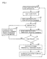
- Fig. 1 is a flowchart schematically showing a typical and exemplary method of manufacturing a silicon-based thin-film photoelectric conversion device according to the present invention.
- a transparent conductive film is formed on a transparent substrate of glass for example.
- the substrate is fed into a plasma CVD apparatus.
- the transparent conductive film of SnO 2 for example is used here.
- a transparent conductive oxide film of ITO or ZnO for example may be used.
- the substrate fed into the plasma CVD apparatus is heated to and kept at a film deposition temperature for a certain period of time in the heating chamber.
- a p-type semiconductor layer is first deposited by plasma CVD on the transparent conductive film.
- this p-type semiconductor layer is deposited under the condition that the heating temperature of the substrate in the film deposition chamber is at most 550°C and to a thickness of at least 2 nm and at most 50 nm.
- a source gas supplied into the film deposition chamber has main components that are for example such a silane-based gas as silane gas and a diluent gas of hydrogen gas for example. Further, preferably the flow rate of the diluent gas is at least 100 times as high as the flow rate of the silane-based gas and diborane is used as a doping gas.
- the p-type semiconductor layer may be a p-type amorphous or microcrystalline silicon thin-film that is doped for example with boron, which is impurity atom determining the conductivity type, of at least 1 atomic percent and at most 5 atomic percent.
- boron which is impurity atom determining the conductivity type, of at least 1 atomic percent and at most 5 atomic percent.
- impurity atoms as aluminum atoms may be used.
- the p-type layer may be a layer of such an alloy as amorphous or microcrystalline silicon carbide or amorphous silicon germanium.
- the thickness of the p-type layer may be any in the range from 2 nm to 50 nm inclusive.
- the p-type semiconductor layer may be a polycrystalline silicon-based thin-film, an alloy-based thin-film, or a multilayer of a plurality of different thin films.
- an i-type microcrystalline silicon-based photoelectric conversion layer and an n-type semiconductor layer are deposited in this order on the p-type semiconductor layer in the same film deposition chamber with plasma CVD.
- the i-type microcrystalline silicon-based photoelectric conversion layer is deposited to a thickness of at least 0.5 ⁇ m and at most 20 ⁇ m
- the n-type semiconductor layer is deposited to a thickness of at least 2 nm and at most 50 nm.
- the i-type photoelectric conversion layer is preferably deposited under the conditions that the heating temperature of the substrate is at most 550°C and the flow rate of a diluent gas is at least 30 times and at most 100 times as high as the flow rate of a silane-based gas. Further, the peak intensity ratio at 480 nm -1 and 520 nm -1 measured by Raman spectroscopy, I 520 /I 480 , is at least 5 and at most 10.
- the microcrystalline silicon-based thin-film may be an i-type microcrystalline silicon thin-film or a weak p-type or weak n-type microcrystalline silicon thin-film having a satisfactory photoelectric conversion function.
- the photoelectric conversion layer is not limited to the above-described ones. For example, an alloy layer of silicon carbide or silicon germanium may be used as well.
- n-type semiconductor layer an n-type amorphous or microcrystalline silicon-based thin-film doped with phosphorus, if impurity atoms determining the conductivity type are phosphorus atoms, of at least 0.1 atomic percent and at most 5 atomic percent, for example.
- the conditions concerning the n-type semiconductor layer are not limitations.
- An alloy layer of microcrystalline silicon carbide or silicon germanium for example may be used.
- the thickness of the n-type semiconductor layer is appropriately in the range from 2 nm to 50 nm inclusive.
- the substrate is fed into the temporary reserve chamber. Then, in S6, it is checked whether such abnormality as peeling of films from a cathode occurs. If any abnormality is found (YES in S6), the manufacturing process proceeds to S7 and preferably the cathode is etched for removing all the remaining films on the cathode and the surface of the electrode is made stable (predeposited) in S8. If there is no abnormality (NO in S6), the process proceeds to S9 to etch the film deposition chamber and eliminate influences of remaining n-type impurities attached within the film deposition chamber when the final n-layer has been deposited. Remaining n-type impurities may be removed by plasma decomposition of hydrogen gas, inert gas, fluorine-based cleaning gas or an arbitrary mixture thereof.
- influences of n-type impurities are eliminated by first etching away an n-layer deposited within the film deposition chamber and thereafter etching away an i-layer by at least 10 nm in thickness and at most a half of the thickness of the i-layer. After influences of the remaining n-type impurities are completely eliminated, a subsequent substrate is fed into the same film deposition chamber so that the pin layers can repeatedly be deposited. When the step of depositing the pin layers is repeated multiple times (pin deposition number), remaining films of the number corresponding to the pin deposition number that have not been etched away are stacked on the cathode.
- all the remaining films on the cathode are removed for removing point defects on the substrate. Further, in order to prevent occurrence of such detects, preferably all the remaining films are removed when the total thickness of the remaining films on the cathode is at least 10 ⁇ m and at most 1000 ⁇ m.
- the remaining films are removed by plasma decomposition of hydrogen gas, inert gas, fluorine-based cleaning gas or an arbitrary mixture thereof
- the device can be manufactured by the single chamber system so that the manufacturing facilities can be simplified as compared with the inline system or multi-chamber system.
- the apparatus can be operated for a long period of time without opening the film deposition chamber. Therefore, the tact time in manufacture can significantly be shortened to reduce the production cost.
- Fig. 5 is a cross-sectional view schematically showing a structure of a stacked silicon-based thin-film photoelectric conversion device manufactured according to a method of the present invention.
- the stacked photoelectric conversion device includes an amorphous photoelectric conversion device 12, 13, 14 and a microcrystalline photoelectric conversion device 7, 8, 9 stacked via a transparent conductive film 10 on a substrate 11.
- the stacked photoelectric conversion device includes a back electrode unit comprised of a conductive film 6 and a metal electrode 5.
- the amorphous photoelectric conversion device includes a p-type semiconductor layer 14, an i-type amorphous photoelectric conversion layer 13 and an n-type semiconductor layer 12.
- the microcrystalline photoelectric conversion device is produced by a similar method to that of the photoelectric conversion device shown.in Fig. 3. Specifically, the microcrystalline photoelectric conversion device includes a p-type semiconductor layer 9, an i-type microcrystalline photoelectric conversion layer 8 and an n-type semiconductor layer 7. Similarly, conductive film 6 of ZnO for example and metal electrode 5 of Ag for example may be used.
- Example 1 silicon-based thin-film photoelectric conversion devices having the structure shown in Fig. 3 were successively manufactured through the manufacturing process repeated multiple times.
- a first silicon-based thin-film photoelectric conversion device was manufactured by forming transparent conductive film 10 of SnO 2 on substrate 11 of glass and thereafter depositing boron-doped p-type semiconductor layer 9 of microcrystalline silicon with a thickness of 10 nm, non-doped i-type photoelectric conversion layer 8 of microcrystalline silicon with a thickness of 3 ⁇ m and phosphorus-doped n-type semiconductor layer 7 of silicon with a thickness of 20 nm in this order on transparent conductive film 10.
- conductive film 6 of ZnO with a thickness of 50 nm and metal electrode 5 of Ag with a thickness of 300 nm were formed so that a back electrode unit comprised of conductive film 6 and metal electrode 5 was provided.
- the first silicon-based photoelectric conversion device was produced.
- the pin layers of the photoelectric conversion device were deposited in the same film deposition chamber with RF plasma CVD under the following conditions.
- silane and hydrogen were used as a film-deposition gas.
- diborane of 0.5 atomic percent with respect to silane was added in depositing the p-type silicon layer and phosphine of 0.3 atomic percent with respect to silane was added in depositing the n-type silicon layer.
- the heating temperature of the substrate was set to 200°C while the flow rate ratio between the silane gas and hydrogen gas was set to 1 : 150.
- the heating temperature of the substrate was set to 200°C while the flow rate ratio between the silane gas and hydrogen gas was set to 1 : 70.
- the heating temperature of the substrate was set to 200°C while the flow rate ratio between silane gas and hydrogen gas was set to 1 : 50.
- the photoelectric conversion efficiency of the silicon-based thin-film photoelectric conversion device thus produced was measured by irradiating the device with pseudo sunlight of AM 1.5, 100 mW/cm 2 with a solar simulator. The measured photoelectric conversion efficiency was 8.3 %.
- the substrate was then removed from the film deposition chamber. Then, to this chamber, as an etching gas and a diluent gas, nitrogen trifluoride and argon of 20 volume % in concentration were supplied for etching of the inside of the film deposition chamber under a pressure of 67 Pa.
- the etch rate at this time was at least 10 nm/s so that an n-layer and an i-layer of 50 nm in thickness were etched.
- a subsequent substrate was fed into the film deposition chamber.
- a second silicon-based thin-film photoelectric conversion device with the pin junction was produced by depositing pin layers as done for the first pin layers. Specifically, a boron-doped p-type silicon layer with a thickness of 10 nm, a non-doped i-type microcrystalline silicon photoelectric conversion layer with a thickness of 3 ⁇ m and a phosphorus-doped n-type silicon layer with a thickness of 20 nm were deposited by RF plasma CVD.
- the silicon layers of the pin in the photoelectric conversion device were deposited in the same film deposition chamber by RF plasma CVD.
- a source gas of silane and hydrogen was used.
- diborane of 0.5 atomic percent with respect to silane was added.
- phosphine of 0.3 atomic percent with respect to silane was added.
- the heating temperature of the substrate was set to 200°C while the flow rate ratio between the silane gas and the hydrogen gas was set to 1 : 150.
- the heating temperature of the substrate was set to 200 °C while the flow rate ratio between the silane gas and the hydrogen gas was set to 1 : 70.
- the heating temperature of the substrate was set to 200°C while the flow rate ratio between the silane gas and the hydrogen gas was set to 1 : 50.
- a conductive film of ZnO with a thickness of 50 nm and a metal electrode of Ag with a thickness of 300 nm were produced by sputtering to provide a back electrode unit.
- the photoelectric conversion efficiency of the second silicon-based thin-film photoelectric conversion device thus produced was measured by irradiating the device with pseudo sunlight of AM 1.5, 100 mW/cm 2 with the solar simulator. The measured photoelectric conversion efficiency was 8.4 %.
- the pin deposition was repeated in the same film deposition chamber.
- Fig. 4 shows a relation between the number of times the pin deposition was done and the photoelectric conversion efficiency. It is seen from Fig. 4 that even after the tenth pin deposition was done, no significant characteristic change occurs. Further, a good manufacturing yield, 100 % was achieved regardless of the number of times the deposition was done.
- a silicon-based thin-film photoelectric conversion device was produced similarly to that of Example 1 except that first pin layers were deposited on a substrate, then the substrate was removed from the chamber and subsequently second pin layers were deposited on a subsequent substrate without eliminating influences of remaining n-type impurities.
- the photoelectric conversion efficiency of the photoelectric conversion device with the secondly deposited pin layers was measured by a similar method to that in Example 1.
- the photoelectric conversion efficiency thus measured was 4.8 % which was considerably lower than that in Example 1, while a good manufacturing yield of approximately 100 % was still achieved.
- a comparison of spectral sensitivity curve was made between the photoelectric conversion device with the secondly deposited pin layers in Example 1 and the photoelectric conversion device with the secondly deposited pin layers in Comparative Example 1. Comparative Example 1 exhibited a significant deterioration in shortwave sensitivity as compared with Example 1.
- Deposition of pin layers was successively done approximately 50 times under the conditions employed in Example 1 and consequently the total thickness of films remaining impurities stacked on the cathode reached 150 ⁇ m or more. Point detects due to peeling of the remaining films on the cathode were likely to occur and accordingly it was found that the manufacturing yield of photoelectric conversion devices decreases to 30 % or lower. After the yield deterioration due to the peeling of remaining films was confirmed, the remaining films on the cathode were removed under the same conditions as the cleaning conditions used in removing remaining n-type impurities in the film deposition chamber in Example 1.
- etching gas and a diluent gas nitrogen trifluoride and argon gas of 20 volume % in concentration were supplied and etching was done under a pressure of 67 Pa.
- the resultant etch rate was 10 nm/s or higher so that all the stacked films with a thickness of 150 ⁇ m on the cathode resultant from 50 depositions of the pin layers could be etched away.
- a dummy substrate was fed into the chamber for making the surface of the cathode electrode stable, and a layer of 1 ⁇ m in thickness was formed under the same conditions for the i-layer.
- a photoelectric conversion device including an amorphous silicon-based photoelectric conversion layer On a photoelectric conversion device including an amorphous silicon-based photoelectric conversion layer, a photoelectric conversion device including a microcrystalline silicon-based photoelectric conversion layer that was firstly produced by a similar method to that in Example 1 was stacked to produce a stacked photoelectric conversion device having the structure as shown in Fig. 5. The photoelectric conversion efficiency of the stacked photoelectric conversion device was measured in a similar manner to that in Example 1 and the measurement was 12.5 %. After this, by a method similar to that in Example 1, the cleaning process was followed for removing remaining n-type impurities. Then, a photoelectric conversion device having a microcrystalline silicon-based photoelectric conversion layer that was secondly produced was obtained.
- This photoelectric conversion device was then stacked on a photoelectric conversion device including an amorphous silicon-based photoelectric conversion layer to obtain a stacked photoelectric conversion device as shown in Fig. 5.
- the photoelectric conversion efficiency measured by a similar method to that in Example 1 was 12.4 %, which was an almost equivalent characteristic to that of the firstly produced stacked photoelectric conversion device including the microcrystalline silicon-based photoelectric conversion layer.
- influences of remaining n-type impurities in the film deposition chamber were eliminated while pin layers were repeatedly deposited in the same film deposition chamber.
- Fig. 4 shows a relation between the number of times film deposition is made and photoelectric conversion efficiency. As seen from Fig. 4, no significant characteristic change occurs even after the tenth deposition was done. Further, the manufacturing yield was still good, which was 100 %.
Landscapes
- Photovoltaic Devices (AREA)
Applications Claiming Priority (2)
| Application Number | Priority Date | Filing Date | Title |
|---|---|---|---|
| JP2003358091 | 2003-10-17 | ||
| JP2003358091A JP2005123466A (ja) | 2003-10-17 | 2003-10-17 | シリコン系薄膜光電変換装置の製造方法およびその方法により製造されたシリコン系薄膜光電変換装置 |
Publications (3)
| Publication Number | Publication Date |
|---|---|
| EP1524703A2 true EP1524703A2 (fr) | 2005-04-20 |
| EP1524703A3 EP1524703A3 (fr) | 2007-10-10 |
| EP1524703B1 EP1524703B1 (fr) | 2010-09-29 |
Family
ID=34373637
Family Applications (1)
| Application Number | Title | Priority Date | Filing Date |
|---|---|---|---|
| EP04023803A Expired - Lifetime EP1524703B1 (fr) | 2003-10-17 | 2004-10-06 | Procédé de fabrication d'une cellule solaire à base de Si |
Country Status (4)
| Country | Link |
|---|---|
| US (1) | US6979589B2 (fr) |
| EP (1) | EP1524703B1 (fr) |
| JP (1) | JP2005123466A (fr) |
| DE (1) | DE602004029318D1 (fr) |
Families Citing this family (22)
| Publication number | Priority date | Publication date | Assignee | Title |
|---|---|---|---|---|
| US20100147379A1 (en) * | 2005-10-03 | 2010-06-17 | Katsushi Kishimoto | Silicon-based thin-film photoelectric conversion device, and method and apparatus for manufacturing the same |
| JP2007214283A (ja) * | 2006-02-08 | 2007-08-23 | Sanyo Electric Co Ltd | 光起電力素子 |
| JP2007281018A (ja) * | 2006-04-03 | 2007-10-25 | Mitsubishi Heavy Ind Ltd | 光電変換装置及びその製造方法 |
| US20080023070A1 (en) * | 2006-07-28 | 2008-01-31 | Sanjai Sinha | Methods and systems for manufacturing polycrystalline silicon and silicon-germanium solar cells |
| JP4954014B2 (ja) * | 2006-10-23 | 2012-06-13 | キヤノン株式会社 | 堆積膜形成方法及び光起電力素子の形成方法 |
| US8203071B2 (en) | 2007-01-18 | 2012-06-19 | Applied Materials, Inc. | Multi-junction solar cells and methods and apparatuses for forming the same |
| US8142606B2 (en) * | 2007-06-07 | 2012-03-27 | Applied Materials, Inc. | Apparatus for depositing a uniform silicon film and methods for manufacturing the same |
| US7875486B2 (en) * | 2007-07-10 | 2011-01-25 | Applied Materials, Inc. | Solar cells and methods and apparatuses for forming the same including I-layer and N-layer chamber cleaning |
| US20090104733A1 (en) * | 2007-10-22 | 2009-04-23 | Yong Kee Chae | Microcrystalline silicon deposition for thin film solar applications |
| WO2009059238A1 (fr) | 2007-11-02 | 2009-05-07 | Applied Materials, Inc. | Traitement au plasma entre des procédés de dépôt |
| JP5330723B2 (ja) * | 2008-03-28 | 2013-10-30 | 三菱重工業株式会社 | 光電変換装置 |
| JP4573902B2 (ja) * | 2008-03-28 | 2010-11-04 | 三菱電機株式会社 | 薄膜形成方法 |
| WO2009128522A1 (fr) * | 2008-04-18 | 2009-10-22 | Semiconductor Energy Laboratory Co., Ltd. | Transistor a couches minces et procede de fabrication associe |
| CN102007585B (zh) * | 2008-04-18 | 2013-05-29 | 株式会社半导体能源研究所 | 薄膜晶体管及其制造方法 |
| US8053294B2 (en) * | 2008-04-21 | 2011-11-08 | Semiconductor Energy Laboratory Co., Ltd. | Manufacturing method of thin film transistor by controlling generation of crystal nuclei of microcrystalline semiconductor film |
| JP5436017B2 (ja) * | 2008-04-25 | 2014-03-05 | 株式会社半導体エネルギー研究所 | 半導体装置 |
| WO2009157573A1 (fr) * | 2008-06-27 | 2009-12-30 | Semiconductor Energy Laboratory Co., Ltd. | Transistor à couche mince, dispositif semi-conducteur et dispositif électronique |
| US20110088760A1 (en) * | 2009-10-20 | 2011-04-21 | Applied Materials, Inc. | Methods of forming an amorphous silicon layer for thin film solar cell application |
| WO2011084381A2 (fr) * | 2009-12-21 | 2011-07-14 | Applied Materials, Inc. | Optimisation du nettoyage de couches solaires par dépôt chimique en phase vapeur assisté par plasma |
| JP2011222929A (ja) * | 2010-03-23 | 2011-11-04 | Toshiba Corp | 不揮発性記憶装置及びその製造方法 |
| US8895435B2 (en) * | 2011-01-31 | 2014-11-25 | United Microelectronics Corp. | Polysilicon layer and method of forming the same |
| US9105769B2 (en) | 2013-09-12 | 2015-08-11 | International Business Machines Corporation | Shallow junction photovoltaic devices |
Citations (4)
| Publication number | Priority date | Publication date | Assignee | Title |
|---|---|---|---|---|
| JPS5992519A (ja) | 1982-11-19 | 1984-05-28 | Hitachi Ltd | 半導体装置の製造方法 |
| JP2000243993A (ja) | 1999-02-24 | 2000-09-08 | Kanegafuchi Chem Ind Co Ltd | シリコン系薄膜光電変換装置の製造方法 |
| JP2000252495A (ja) | 1999-02-26 | 2000-09-14 | Kanegafuchi Chem Ind Co Ltd | シリコン系薄膜光電変換装置の製造方法 |
| US6337224B1 (en) | 1997-11-10 | 2002-01-08 | Kaneka Corporation | Method of producing silicon thin-film photoelectric transducer and plasma CVD apparatus used for the method |
Family Cites Families (6)
| Publication number | Priority date | Publication date | Assignee | Title |
|---|---|---|---|---|
| JPH04165075A (ja) * | 1990-10-25 | 1992-06-10 | Canon Inc | 化学蒸着装置のクリーニング法 |
| MX9202941A (es) * | 1991-06-18 | 1993-02-01 | Advanced Photovoltaic Systems | Pelicula de silicio amorfo, metodo para su fabricacion y dispositivo fotovoltaico. |
| CA2102948C (fr) * | 1992-11-16 | 1998-10-27 | Keishi Saito | Convertisseur photoelectrique et systeme generateur d'energie |
| US6626185B2 (en) * | 1996-06-28 | 2003-09-30 | Lam Research Corporation | Method of depositing a silicon containing layer on a semiconductor substrate |
| EP1154038A1 (fr) * | 2000-05-12 | 2001-11-14 | Applied Materials, Inc. | Méthode de conditionnement d'un réacteur CVD |
| US6436488B1 (en) * | 2000-06-12 | 2002-08-20 | Agilent Technologies, Inc. | Chemical vapor deposition method for amorphous silicon and resulting film |
-
2003
- 2003-10-17 JP JP2003358091A patent/JP2005123466A/ja active Pending
-
2004
- 2004-09-17 US US10/942,958 patent/US6979589B2/en not_active Expired - Fee Related
- 2004-10-06 EP EP04023803A patent/EP1524703B1/fr not_active Expired - Lifetime
- 2004-10-06 DE DE602004029318T patent/DE602004029318D1/de not_active Expired - Lifetime
Patent Citations (4)
| Publication number | Priority date | Publication date | Assignee | Title |
|---|---|---|---|---|
| JPS5992519A (ja) | 1982-11-19 | 1984-05-28 | Hitachi Ltd | 半導体装置の製造方法 |
| US6337224B1 (en) | 1997-11-10 | 2002-01-08 | Kaneka Corporation | Method of producing silicon thin-film photoelectric transducer and plasma CVD apparatus used for the method |
| JP2000243993A (ja) | 1999-02-24 | 2000-09-08 | Kanegafuchi Chem Ind Co Ltd | シリコン系薄膜光電変換装置の製造方法 |
| JP2000252495A (ja) | 1999-02-26 | 2000-09-14 | Kanegafuchi Chem Ind Co Ltd | シリコン系薄膜光電変換装置の製造方法 |
Also Published As
| Publication number | Publication date |
|---|---|
| EP1524703B1 (fr) | 2010-09-29 |
| JP2005123466A (ja) | 2005-05-12 |
| US6979589B2 (en) | 2005-12-27 |
| EP1524703A3 (fr) | 2007-10-10 |
| US20050085003A1 (en) | 2005-04-21 |
| DE602004029318D1 (de) | 2010-11-11 |
Similar Documents
| Publication | Publication Date | Title |
|---|---|---|
| US6979589B2 (en) | Silicon-based thin-film photoelectric conversion device and method of manufacturing thereof | |
| US6566159B2 (en) | Method of manufacturing tandem thin-film solar cell | |
| KR101521326B1 (ko) | 태양 전지 | |
| EP0994515B1 (fr) | Méthode de fabrication d'un dispositif de conversion photoélectrique en couche mince à base de silicium | |
| JP3589581B2 (ja) | タンデム型の薄膜光電変換装置の製造方法 | |
| JP2951146B2 (ja) | 光起電力デバイス | |
| EP1032052B1 (fr) | Procédé de la fabrication d'une cellule solaire en couche mince à base de silicium | |
| KR101057208B1 (ko) | 실리콘계 박막 광전 변환 장치, 그 제조 방법 및 그 제조장치 | |
| US20070023082A1 (en) | Compositionally-graded back contact photovoltaic devices and methods of fabricating such devices | |
| WO2007018934A2 (fr) | Dispositif photovoltaique a composition echelonnee, procede de fabrication dudit dispositif et articles associes | |
| AU2007202844A1 (en) | Photovoltaic device which includes all-back-contact configuration; and related processes | |
| US20080245414A1 (en) | Methods for forming a photovoltaic device with low contact resistance | |
| CN108431967B (zh) | 光电转换装置的制造方法 | |
| CN108475707A (zh) | 光电转换装置的制造方法 | |
| EP2323172A1 (fr) | Procédé de fabrication d'un dispositif de conversion photoélectrique, dispositif de conversion photoélectrique, et système de fabrication d'un dispositif de conversion photoélectrique | |
| US20250072154A1 (en) | Solar cell and method for forming the same | |
| JP4358343B2 (ja) | シリコン系薄膜光電変換装置の製造方法 | |
| US4845043A (en) | Method for fabricating photovoltaic device having improved short wavelength photoresponse | |
| JP2000243992A (ja) | シリコン系薄膜光電変換装置の製造方法 | |
| JP3746607B2 (ja) | シリコン系薄膜光電変換装置の製造方法 | |
| JP3753528B2 (ja) | シリコン系薄膜光電変換装置の製造方法 | |
| KR101100109B1 (ko) | 광기전력 장치의 제조 방법 | |
| JP2004253417A (ja) | 薄膜太陽電池の製造方法 | |
| JPH06177409A (ja) | 薄膜太陽電池の製造方法 | |
| JPH11330515A (ja) | シリコン系薄膜光電変換装置の製造方法 |
Legal Events
| Date | Code | Title | Description |
|---|---|---|---|
| PUAI | Public reference made under article 153(3) epc to a published international application that has entered the european phase |
Free format text: ORIGINAL CODE: 0009012 |
|
| AK | Designated contracting states |
Kind code of ref document: A2 Designated state(s): AT BE BG CH CY CZ DE DK EE ES FI FR GB GR HU IE IT LI LU MC NL PL PT RO SE SI SK TR |
|
| AX | Request for extension of the european patent |
Extension state: AL HR LT LV MK |
|
| PUAL | Search report despatched |
Free format text: ORIGINAL CODE: 0009013 |
|
| AK | Designated contracting states |
Kind code of ref document: A3 Designated state(s): AT BE BG CH CY CZ DE DK EE ES FI FR GB GR HU IE IT LI LU MC NL PL PT RO SE SI SK TR |
|
| AX | Request for extension of the european patent |
Extension state: AL HR LT LV MK |
|
| RIC1 | Information provided on ipc code assigned before grant |
Ipc: C23C 16/44 20060101ALI20070904BHEP Ipc: H01L 31/18 20060101AFI20041115BHEP |
|
| 17P | Request for examination filed |
Effective date: 20071107 |
|
| AKX | Designation fees paid |
Designated state(s): DE GB |
|
| 17Q | First examination report despatched |
Effective date: 20090309 |
|
| GRAP | Despatch of communication of intention to grant a patent |
Free format text: ORIGINAL CODE: EPIDOSNIGR1 |
|
| GRAS | Grant fee paid |
Free format text: ORIGINAL CODE: EPIDOSNIGR3 |
|
| GRAA | (expected) grant |
Free format text: ORIGINAL CODE: 0009210 |
|
| AK | Designated contracting states |
Kind code of ref document: B1 Designated state(s): DE GB |
|
| REG | Reference to a national code |
Ref country code: GB Ref legal event code: FG4D |
|
| REF | Corresponds to: |
Ref document number: 602004029318 Country of ref document: DE Date of ref document: 20101111 Kind code of ref document: P |
|
| PLBE | No opposition filed within time limit |
Free format text: ORIGINAL CODE: 0009261 |
|
| STAA | Information on the status of an ep patent application or granted ep patent |
Free format text: STATUS: NO OPPOSITION FILED WITHIN TIME LIMIT |
|
| 26N | No opposition filed |
Effective date: 20110630 |
|
| REG | Reference to a national code |
Ref country code: DE Ref legal event code: R097 Ref document number: 602004029318 Country of ref document: DE Effective date: 20110630 |
|
| PGFP | Annual fee paid to national office [announced via postgrant information from national office to epo] |
Ref country code: DE Payment date: 20121003 Year of fee payment: 9 |
|
| PGFP | Annual fee paid to national office [announced via postgrant information from national office to epo] |
Ref country code: GB Payment date: 20121003 Year of fee payment: 9 |
|
| GBPC | Gb: european patent ceased through non-payment of renewal fee |
Effective date: 20131006 |
|
| REG | Reference to a national code |
Ref country code: DE Ref legal event code: R119 Ref document number: 602004029318 Country of ref document: DE Effective date: 20140501 |
|
| PG25 | Lapsed in a contracting state [announced via postgrant information from national office to epo] |
Ref country code: GB Free format text: LAPSE BECAUSE OF NON-PAYMENT OF DUE FEES Effective date: 20131006 |
|
| PG25 | Lapsed in a contracting state [announced via postgrant information from national office to epo] |
Ref country code: DE Free format text: LAPSE BECAUSE OF NON-PAYMENT OF DUE FEES Effective date: 20140501 |