EP1526761A2 - Circuit pour alimenter une lampe à barrière diélectrique muni d'une protection contre les surtensions - Google Patents
Circuit pour alimenter une lampe à barrière diélectrique muni d'une protection contre les surtensions Download PDFInfo
- Publication number
- EP1526761A2 EP1526761A2 EP04022966A EP04022966A EP1526761A2 EP 1526761 A2 EP1526761 A2 EP 1526761A2 EP 04022966 A EP04022966 A EP 04022966A EP 04022966 A EP04022966 A EP 04022966A EP 1526761 A2 EP1526761 A2 EP 1526761A2
- Authority
- EP
- European Patent Office
- Prior art keywords
- lamp
- dbd
- switching transistor
- operating circuit
- converter
- Prior art date
- Legal status (The legal status is an assumption and is not a legal conclusion. Google has not performed a legal analysis and makes no representation as to the accuracy of the status listed.)
- Granted
Links
- 230000004888 barrier function Effects 0.000 title description 2
- 238000012360 testing method Methods 0.000 claims abstract description 17
- 238000000034 method Methods 0.000 claims abstract description 9
- 230000006378 damage Effects 0.000 claims description 9
- 230000008878 coupling Effects 0.000 claims description 3
- 238000010168 coupling process Methods 0.000 claims description 3
- 238000005859 coupling reaction Methods 0.000 claims description 3
- 230000001939 inductive effect Effects 0.000 claims description 3
- 238000001514 detection method Methods 0.000 claims 1
- 238000005286 illumination Methods 0.000 claims 1
- 238000004804 winding Methods 0.000 description 15
- 239000003990 capacitor Substances 0.000 description 5
- 230000006698 induction Effects 0.000 description 5
- 238000002347 injection Methods 0.000 description 4
- 239000007924 injection Substances 0.000 description 4
- 238000010586 diagram Methods 0.000 description 3
- 230000015556 catabolic process Effects 0.000 description 2
- 230000007423 decrease Effects 0.000 description 2
- 230000007246 mechanism Effects 0.000 description 2
- 230000008569 process Effects 0.000 description 2
- 230000001960 triggered effect Effects 0.000 description 2
- 230000003466 anti-cipated effect Effects 0.000 description 1
- 230000000903 blocking effect Effects 0.000 description 1
- 230000008859 change Effects 0.000 description 1
- 238000013461 design Methods 0.000 description 1
- 238000004146 energy storage Methods 0.000 description 1
- 238000010304 firing Methods 0.000 description 1
- 230000005283 ground state Effects 0.000 description 1
- 230000001976 improved effect Effects 0.000 description 1
- 238000012423 maintenance Methods 0.000 description 1
- 238000012544 monitoring process Methods 0.000 description 1
- 230000004044 response Effects 0.000 description 1
- 230000000630 rising effect Effects 0.000 description 1
- 230000029305 taxis Effects 0.000 description 1
Images
Classifications
-
- H—ELECTRICITY
- H05—ELECTRIC TECHNIQUES NOT OTHERWISE PROVIDED FOR
- H05B—ELECTRIC HEATING; ELECTRIC LIGHT SOURCES NOT OTHERWISE PROVIDED FOR; CIRCUIT ARRANGEMENTS FOR ELECTRIC LIGHT SOURCES, IN GENERAL
- H05B41/00—Circuit arrangements or apparatus for igniting or operating discharge lamps
- H05B41/14—Circuit arrangements
- H05B41/26—Circuit arrangements in which the lamp is fed by power derived from DC by means of a converter, e.g. by high-voltage DC
-
- H—ELECTRICITY
- H05—ELECTRIC TECHNIQUES NOT OTHERWISE PROVIDED FOR
- H05B—ELECTRIC HEATING; ELECTRIC LIGHT SOURCES NOT OTHERWISE PROVIDED FOR; CIRCUIT ARRANGEMENTS FOR ELECTRIC LIGHT SOURCES, IN GENERAL
- H05B41/00—Circuit arrangements or apparatus for igniting or operating discharge lamps
- H05B41/14—Circuit arrangements
- H05B41/24—Circuit arrangements in which the lamp is fed by high frequency AC, or with separate oscillator frequency
-
- H—ELECTRICITY
- H05—ELECTRIC TECHNIQUES NOT OTHERWISE PROVIDED FOR
- H05B—ELECTRIC HEATING; ELECTRIC LIGHT SOURCES NOT OTHERWISE PROVIDED FOR; CIRCUIT ARRANGEMENTS FOR ELECTRIC LIGHT SOURCES, IN GENERAL
- H05B41/00—Circuit arrangements or apparatus for igniting or operating discharge lamps
- H05B41/14—Circuit arrangements
- H05B41/26—Circuit arrangements in which the lamp is fed by power derived from DC by means of a converter, e.g. by high-voltage DC
- H05B41/28—Circuit arrangements in which the lamp is fed by power derived from DC by means of a converter, e.g. by high-voltage DC using static converters
- H05B41/288—Circuit arrangements in which the lamp is fed by power derived from DC by means of a converter, e.g. by high-voltage DC using static converters with semiconductor devices and specially adapted for lamps without preheating electrodes, e.g. for high-intensity discharge lamps, high-pressure mercury or sodium lamps or low-pressure sodium lamps
-
- H—ELECTRICITY
- H05—ELECTRIC TECHNIQUES NOT OTHERWISE PROVIDED FOR
- H05B—ELECTRIC HEATING; ELECTRIC LIGHT SOURCES NOT OTHERWISE PROVIDED FOR; CIRCUIT ARRANGEMENTS FOR ELECTRIC LIGHT SOURCES, IN GENERAL
- H05B41/00—Circuit arrangements or apparatus for igniting or operating discharge lamps
- H05B41/14—Circuit arrangements
- H05B41/26—Circuit arrangements in which the lamp is fed by power derived from DC by means of a converter, e.g. by high-voltage DC
- H05B41/28—Circuit arrangements in which the lamp is fed by power derived from DC by means of a converter, e.g. by high-voltage DC using static converters
- H05B41/288—Circuit arrangements in which the lamp is fed by power derived from DC by means of a converter, e.g. by high-voltage DC using static converters with semiconductor devices and specially adapted for lamps without preheating electrodes, e.g. for high-intensity discharge lamps, high-pressure mercury or sodium lamps or low-pressure sodium lamps
- H05B41/292—Arrangements for protecting lamps or circuits against abnormal operating conditions
Definitions
- the present invention relates to a circuit and a method for operating a dielectrically impeded discharge lamp.
- Dielectric barrier discharge lamps are known and draw essentially by the fact that at least a part of the for the Ignition and maintenance of discharge used electrodes is separated from the discharge medium by a dielectric layer. she are sometimes referred to as "silent discharge lamps". Such Discharge lamps are powered by electronic ballasts or more generally spoken operating circuits ignited and operated. I. d. R. are for ignition larger voltages and thus in the power input larger amplitudes necessary than in continuous operation.
- Operating circuits for such lamps regularly include a converter for coupling the power into the lamp.
- such discharge lamps operate with AC power of various kinds, wherein in particular a pulsed mode of operation with time-without power einklplungsbuild Times disconnected power input phases due the resulting efficiency gains are of interest.
- the invention refers in principle but to operating circuits of any kind for dielectric disabled discharge lamps. It is known in a the converter energized line path to switch a switching transistor, the by its switching operation for the ignition process and in the case of a pulsed Continuous power input also responsible for the actual lamp operation is.
- the used converters have i. d. R. an inductive characteristic, specifically, it is i. d. R. transformers with a primary winding, which is energized by said switching transistor with power.
- this switching transistor in the event Protect that a startup is attempted without having a lamp properly connected.
- an energy that, if not at least partially removed from the lamp, in the switching transistor is dissipated.
- It can be a surge protection circuit be used, which is the voltage across this transistor, for example measures the drain-source voltage at a FET, and in the If a threshold is exceeded, the lamp operation stops.
- the invention is based on the technical problem of an operating circuit for a dielectrically impeded discharge lamp with an inductive Converter and an overvoltage protection circuit for a switching transistor and a method of igniting such a dielectrically impeded discharge lamp to improve in such a way that they at an operational start attempt show improved properties when the lamp is missing.
- the invention relates to an operating circuit designed to at a restart of the lamp operation, first at least one test power pulse to put on the converter, which is so small that the destruction of the switching transistor as a result of this test power pulse excluded is, and the overvoltage protection circuit on one by this Test power pulse then generates voltage at the switching transistor, if no lamp is connected, and then does not respond, when the lamp is connected.
- the inventor has found that the described monitoring of the voltage over the switching transistor in practically relevant cases not always sufficient. This is especially the case with larger lamp powers and / or if, due to the circuit, a dissipation in the converter inductance stored energy in only one of possibly several Switching transistors takes place, so early to a destruction of the Switching transistor come that mentioned overvoltage protection circuit does not respond quickly enough.
- the invention therefore goes the way it is before finding that actually a lamp connected properly is not, even for the switching transistor critical energies in let the transducer inductance come. Rather, in one of the lamp ignition initially referred to herein as test power pulses Power pulses are applied to the converter.
- the inductor If the lamp is missing, so the inductor generates a larger induction voltage and generates thus in the switching transistor, a larger current or a greater power loss or a larger voltage drop across the switching transistor as if the lamp is connected and therefore an essential part the energy is removed from the inductance.
- test power pulses can therefore depend on the individual case the anticipated destruction mechanism in terms of voltage, current moderately and / or in terms of performance of the later Zünd elaboratespulsen or Distinguish operating power pulses.
- test power pulse is sufficient for this, preferably however, several such pulses delivered.
- the transducer is constructed so that He works on the flyback principle, so in certain phases through Current flow through an inductance stores energy and this during blocking of the current flow to the discharge lamp emits.
- the Switching transistor thus in the energy storage phases and locks in the Energyeinkopplungsphasen. Is not there a lack of energy input Lamp connection so the switching transistor is at risk, for example in the case of a MOSFET, by one above the allowable operating range lying avalanche breakdown (ie one operation, usually drain-source current outside the Avalanche Save Operating Area (Avalanche SOA)).
- Avalanche SOA Avalanche Save Operating Area
- a digital monoflop For driving the control input of the switching transistor, such as the gate, can be used advantageously a digital monoflop, so a monostable multivibrator that lasts for a certain predetermined time responsive to an input, assumes an initial state that follows This time falls back into a stable ground state. It will be on the Referenced embodiment.
- the size of the test power pulses mentioned can be, for example, by Adjusting a reference value of a comparator affecting the Current through the switching transistor compares with this reference value. In the case the flyback converter then determines when the by the Transducer inductance and the switching transistor flowing current sufficient has reached great value to match for a test performance pulse Amount of energy in the transducer inductance to stand. Also for this is refer to the embodiment.
- the reference value can be advantageously via a microcontroller Taxes.
- the invention further preferably relates to such operating circuits, in which also the timing of the converter by one, and preferably the same, microcontroller is controlled.
- the control of Converter clocking can be via the enable input of the mentioned monoflop take place, as the embodiment shows.
- the mentioned and principally known overvoltage protection circuit is preferably with a peak rectifier, such as a voltage divider circuit, a diode and a capacitor, and a low-pass characteristic, about as a result of having the capacitance of the capacitor cooperating ohmic impedance built.
- a peak rectifier such as a voltage divider circuit, a diode and a capacitor
- a low-pass characteristic about as a result of having the capacitance of the capacitor cooperating ohmic impedance built.
- the invention is also directed to a set of an operating circuit as described above and a suitable one and preferably already connected dielectrically impeded discharge lamp built-up lighting system.
- This lighting system but is also in the not yet connected state, that is about in separate and packaged manner, already the subject of the invention.
- the invention is also preferably directed to the case of a so-called.
- Flat radiator design the discharge lamp, which consists of a flat flat discharge vessel exists and often, but not exclusively, for backlighting is used by monitors.
- the monitor is also aimed at this monitor Invention, wherein the term "monitor” hereby both computer monitors as well TV screens as well as display panels of other types.
- the invention is particularly in large flat radiators and Monitors, for example with a format over 20 "diagonal.
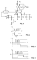
- DBD denotes a dielectrically impeded discharge lamp, which is connected in a secondary circuit with a secondary winding L s of a transformer.
- the transformer has a primary winding Lp which is supplied by a voltage source U zk , the intermediate circuit voltage of an otherwise known and conventional converter. This generates a current flow represented by the arrow and the symbol Ip through the primary winding Lp, which then flows through a lying in series with the primary winding Lp MOSFET T and a shunt resistor R 1 to ground.
- the left-hand gate input of the MOSFET switching transistor T is driven by a monoflop M with an input x and an output y and an enable input e.
- the input x of the monoflop M is in turn driven by a comparator K, at the positive input of a reference voltage U 0 to ground and at its negative input, the voltage between the source terminal of the switching transistor T and the shunt resistor R 1 is applied to ground.
- the tapped off between the primary winding Lp and the switching transistor T voltage to ground is divided down via a voltage divider circuit R 2 , R 3 and placed via a diode D to a connected to its other side to ground capacitor C.
- To the capacitor C is a resistor R 4 in parallel.
- the functioning of the circuit is essentially as follows: When the switching transistor T is conductive, current flows through the primary winding Lp and charges it inductively. If the switching transistor T is blocked, a sudden induction voltage is produced at the primary winding Lp and at the secondary winding L s , which means a power injection pulse for the dielectrically impeded discharge lamp DBD. On the other hand, the induction voltages at the secondary winding L s during the charging phase are below the threshold necessary for a discharge in the lamp DBD.
- the gate input of the switching transistor T is driven by the monoflop M, which operates essentially as summarized in FIG.
- the monoflop M In response to a falling in Fig. 2 above wherein x drawn edge of the input signal changes the output y of the monostable multivibrator M from the high level to the low level and remains at this low level for a certain fixed period of time t from Thereafter, the one-shot falls into the stable Zusand back with high output level.
- This process responds only to the falling edge at the input x and is, as indicated in Fig. 2 above by two different waveforms of the input signal x, completely independent of whether the input signal before or after the end of the time t off again with a rising edge returns to the high level.
- the monoflop M defines the length of the power injection phases of the transformer L p / L s . These power injection phases are triggered via input x. Furthermore, the output of the monoflop M is always low when the enable input e is low. The enable input e releases the monoflop M with a high level state for the described mode of operation.
- the intermediate circuit voltage U zk with the primary circuit current I p charges the primary winding L p of the transformer L p / L s through the switching transistor T and the shunt resistor R 1 until the voltage across the shunt resistor R 1 drops towards Mass reaches the value U 0 and thus generates a sign change of the output of the comparator K.
- the monostable multivibrator M is triggered and locks the switching transistor T for the time t, so that a soupeinkopplungsphase begins.
- the microcontroller which picks up the voltage across the resistor R 4 to ground, suspend further operation and possibly also output a warning signal.
- the microcontroller sets the reference value U 0 clearly high. This generates much larger power pulses, which in a manner known per se lead in a pulsed manner to the ignition of the lamp DBD. After ignition or after a specified ignition phase, the reference value U 0 can be lowered again by the microcontroller to maintain the continuous operation of the lamp DBD with a reference value U 0 , which is greater than the initial, but smaller than the value used during the ignition phase , Of course, the microcontroller may also affect the length of time t out of the monoflop by an internal voltage threshold in the monoflop.
- Figs. 3 and 4 illustrate this in time charts, wherein Fig. 3 shows the prior art.
- the time axis is designated t in both cases.
- the enable signal e is plotted vertically and in the lower area vertically the reference value U 0 .
- the reference value U 0 is lowered in favor of the continuous high-level enable signal recognizable continuous operating state.
- Fig. 4 relates to Fig. 3 and shows in contrast the inventive method.
- the ignition phase of FIG. 3 is preceded by a phase with a very small reference value U 0 , in which pulse bundles are likewise applied which contain test power pulses.
Landscapes
- Circuit Arrangements For Discharge Lamps (AREA)
- Emergency Protection Circuit Devices (AREA)
- Circuit Arrangement For Electric Light Sources In General (AREA)
Applications Claiming Priority (2)
| Application Number | Priority Date | Filing Date | Title |
|---|---|---|---|
| DE10349548 | 2003-10-22 | ||
| DE10349548A DE10349548A1 (de) | 2003-10-22 | 2003-10-22 | Betriebsschaltung für dielektrisch behinderte Entladungslampe mit Überspannungsschutzschaltung |
Publications (3)
| Publication Number | Publication Date |
|---|---|
| EP1526761A2 true EP1526761A2 (fr) | 2005-04-27 |
| EP1526761A3 EP1526761A3 (fr) | 2006-03-29 |
| EP1526761B1 EP1526761B1 (fr) | 2007-04-04 |
Family
ID=34384444
Family Applications (1)
| Application Number | Title | Priority Date | Filing Date |
|---|---|---|---|
| EP04022966A Expired - Lifetime EP1526761B1 (fr) | 2003-10-22 | 2004-09-27 | Circuit pour alimenter une lampe à barrière diélectrique muni d'une protection contre les surtensions |
Country Status (9)
| Country | Link |
|---|---|
| US (1) | US7045973B2 (fr) |
| EP (1) | EP1526761B1 (fr) |
| JP (1) | JP4739723B2 (fr) |
| KR (1) | KR100658233B1 (fr) |
| CN (1) | CN100531505C (fr) |
| AT (1) | ATE358963T1 (fr) |
| CA (1) | CA2485618A1 (fr) |
| DE (2) | DE10349548A1 (fr) |
| TW (1) | TWI285520B (fr) |
Cited By (2)
| Publication number | Priority date | Publication date | Assignee | Title |
|---|---|---|---|---|
| EP1760996A2 (fr) | 2005-08-29 | 2007-03-07 | Samsung Electronics Co., Ltd. | Assemblage à glissière pour un terminal portable |
| EP1753272A3 (fr) * | 2005-07-20 | 2010-01-13 | Patent-Treuhand-Gesellschaft für elektrische Glühlampen mbH | Circuit convertisseur comprenant une inductance au lieu d' un transformateur, pour l' alimentation pulsée d' une lampe à barrière diélectrique. |
Families Citing this family (4)
| Publication number | Priority date | Publication date | Assignee | Title |
|---|---|---|---|---|
| US3049782A (en) * | 1962-08-21 | Ittoesiers | ||
| DE202006004296U1 (de) * | 2006-03-17 | 2006-06-14 | Patent-Treuhand-Gesellschaft für elektrische Glühlampen mbH | Ausschaltzeitregelung |
| US8742677B2 (en) | 2010-01-11 | 2014-06-03 | System General Corp. | LED drive circuit with a programmable input for LED lighting |
| US10778082B2 (en) * | 2018-06-08 | 2020-09-15 | Stmicroelectronics International N.V. | Control circuitry for increasing power output in quasi-resonant converters |
Family Cites Families (16)
| Publication number | Priority date | Publication date | Assignee | Title |
|---|---|---|---|---|
| US4350935A (en) * | 1980-03-28 | 1982-09-21 | Lutron Electronics Co., Inc. | Gas discharge lamp control |
| JPH02199797A (ja) * | 1989-01-26 | 1990-08-08 | Matsushita Electric Works Ltd | 放電灯点灯装置 |
| US5982106A (en) * | 1992-02-24 | 1999-11-09 | Bobel; Andrzej | Self-protected series resonant electronic energy converter |
| JPH05242982A (ja) * | 1992-02-28 | 1993-09-21 | Toshiba Lighting & Technol Corp | 放電灯点灯装置及びこれを用いた照明器具 |
| US6274987B1 (en) * | 1996-05-08 | 2001-08-14 | Magnetek, Inc. | Power sensing lamp protection circuit for ballasts driving gas discharge lamps |
| DE19715342C1 (de) * | 1997-04-12 | 1998-12-17 | Vossloh Schwabe Gmbh | Vorschaltgerät für unabhängigen Parallelbetrieb von Niederdruck-Gasentladungslampen |
| DE19819027A1 (de) * | 1998-04-29 | 1999-11-04 | Patent Treuhand Ges Fuer Elektrische Gluehlampen Mbh | Schaltungsanordnung zum Betrieb mindestens einer Entladungslampe |
| DE19839336A1 (de) * | 1998-08-28 | 2000-03-09 | Patent Treuhand Ges Fuer Elektrische Gluehlampen Mbh | Elektronisches Vorschaltgerät für Entladungslampe mit dielektrisch behinderten Entladungen |
| JP3820791B2 (ja) * | 1999-02-18 | 2006-09-13 | ウシオ電機株式会社 | 誘電体バリア放電ランプ光源装置 |
| JP2002231478A (ja) * | 2000-11-29 | 2002-08-16 | Harison Toshiba Lighting Corp | 放電ランプ点灯装置および機器 |
| DE10115279A1 (de) * | 2000-03-31 | 2001-10-18 | Toshiba Lighting & Technology | Entladungslampenlicht und Leuchteinrichtung hierfür |
| JP4190734B2 (ja) * | 2001-01-15 | 2008-12-03 | ウシオ電機株式会社 | 誘電体バリア放電ランプ光源装置 |
| JP4734740B2 (ja) * | 2001-03-15 | 2011-07-27 | パナソニック電工株式会社 | 電源装置および放電灯点灯装置 |
| KR20030004636A (ko) * | 2001-07-06 | 2003-01-15 | 주식회사 피엔케이텍 | 전자식 안정기 |
| JP2003036987A (ja) * | 2001-07-24 | 2003-02-07 | Harison Toshiba Lighting Corp | 放電ランプ点灯装置、機器および画像形成装置 |
| US6781326B2 (en) * | 2001-12-17 | 2004-08-24 | Q Technology Incorporated | Ballast with lamp sensor and method therefor |
-
2003
- 2003-10-22 DE DE10349548A patent/DE10349548A1/de not_active Withdrawn
-
2004
- 2004-09-27 EP EP04022966A patent/EP1526761B1/fr not_active Expired - Lifetime
- 2004-09-27 AT AT04022966T patent/ATE358963T1/de active
- 2004-09-27 DE DE502004003381T patent/DE502004003381D1/de not_active Expired - Lifetime
- 2004-10-14 US US10/963,535 patent/US7045973B2/en not_active Expired - Lifetime
- 2004-10-18 JP JP2004303446A patent/JP4739723B2/ja not_active Expired - Fee Related
- 2004-10-20 TW TW093131748A patent/TWI285520B/zh not_active IP Right Cessation
- 2004-10-20 CA CA002485618A patent/CA2485618A1/fr not_active Abandoned
- 2004-10-21 KR KR1020040084332A patent/KR100658233B1/ko not_active Expired - Fee Related
- 2004-10-22 CN CNB200410087042XA patent/CN100531505C/zh not_active Expired - Fee Related
Cited By (2)
| Publication number | Priority date | Publication date | Assignee | Title |
|---|---|---|---|---|
| EP1753272A3 (fr) * | 2005-07-20 | 2010-01-13 | Patent-Treuhand-Gesellschaft für elektrische Glühlampen mbH | Circuit convertisseur comprenant une inductance au lieu d' un transformateur, pour l' alimentation pulsée d' une lampe à barrière diélectrique. |
| EP1760996A2 (fr) | 2005-08-29 | 2007-03-07 | Samsung Electronics Co., Ltd. | Assemblage à glissière pour un terminal portable |
Also Published As
| Publication number | Publication date |
|---|---|
| KR100658233B1 (ko) | 2006-12-14 |
| KR20050039606A (ko) | 2005-04-29 |
| DE502004003381D1 (de) | 2007-05-16 |
| JP2005129523A (ja) | 2005-05-19 |
| US7045973B2 (en) | 2006-05-16 |
| JP4739723B2 (ja) | 2011-08-03 |
| ATE358963T1 (de) | 2007-04-15 |
| CA2485618A1 (fr) | 2005-04-22 |
| EP1526761A3 (fr) | 2006-03-29 |
| US20050088116A1 (en) | 2005-04-28 |
| CN100531505C (zh) | 2009-08-19 |
| TW200527974A (en) | 2005-08-16 |
| CN1610476A (zh) | 2005-04-27 |
| TWI285520B (en) | 2007-08-11 |
| DE10349548A1 (de) | 2005-05-25 |
| EP1526761B1 (fr) | 2007-04-04 |
Similar Documents
| Publication | Publication Date | Title |
|---|---|---|
| DE69628739T2 (de) | Steuerung und überwachung von dimmbaren vorschaltgeräten mit breitem beleuchtungshub | |
| EP1333707B1 (fr) | Ballast électronique pour une lampe à décharge | |
| DE60308117T2 (de) | Entladungslampe-Zündungsschaltkreis mit Schutzschaltung | |
| DE4017415C2 (de) | Schaltungsanordnung zum Betrieb einer Hochdruck-Entladungslampe für einen Fahrzeugscheinwerfer | |
| DE19531966C2 (de) | Stromversorgungsschaltung für eine Hochdruck-Entladungslampe | |
| EP1526622B1 (fr) | Ballast électronique avec circuit de protection pour transistors de commutation d'un convertisseur | |
| AT14074U1 (de) | Betriebsschaltung für LED | |
| DE19849738A1 (de) | Impulsgenerator und Vorrichtung zum Betreiben einer Entladungslampe, in der selbiger verwendet wird | |
| EP1526761B1 (fr) | Circuit pour alimenter une lampe à barrière diélectrique muni d'une protection contre les surtensions | |
| EP2138015B1 (fr) | Circuit permettant de produire une tension auxiliaire et de faire fonctionner au moins une lampe à décharge | |
| DE102014216030A1 (de) | Zündsystem und Verfahren zum Betreiben eines Zündsystems | |
| DE19715341C1 (de) | Elektronisches Vorschaltgerät mit automatischem Wiederanlauf | |
| CH664048A5 (de) | Schutzschaltung fuer eine wechselrichterschaltung. | |
| EP2524581B1 (fr) | Montage et procédé permettant de mettre en marche et de faire fonctionner une lampe à décharge haute pression | |
| EP0587602B1 (fr) | Dispositif pour l'exploitation d'une lampe a decharge | |
| EP1395094A1 (fr) | Appareil et procédé permettant de faire fonctionner une lampe | |
| EP1472776B1 (fr) | Dispositif de commutation pour corriger le facteur de puissance | |
| DE19715259A1 (de) | Speisespannungserzeugung an einem Wandler | |
| EP1813135A1 (fr) | Circuit pour faire fonctionner une lampe a decharge a haute pression | |
| AT390156B (de) | Schutzschaltung fuer eine wechselrichterschaltung | |
| WO2005107339A1 (fr) | Dispositif pour produire un train d'impulsions de tension electrique, notamment pour faire fonctionner des lampes a decharge capacitive | |
| EP1583403A1 (fr) | Ballast pour au moins une lampe | |
| EP2208402B1 (fr) | Ballast pour lampe à décharge, par exemple pour une lampe dhi | |
| DE3405769A1 (de) | Verfahren und vorrichtung zum ansteuern des stromleitenden zustandes eines abschaltbaren thyristors | |
| DE19642947A1 (de) | Gleichstrom-Gasentladungslampenstarter und Gleichstrom-Vorschaltgerät für eine Gasentladungslampe |
Legal Events
| Date | Code | Title | Description |
|---|---|---|---|
| PUAI | Public reference made under article 153(3) epc to a published international application that has entered the european phase |
Free format text: ORIGINAL CODE: 0009012 |
|
| AK | Designated contracting states |
Kind code of ref document: A2 Designated state(s): AT BE BG CH CY CZ DE DK EE ES FI FR GB GR HU IE IT LI LU MC NL PL PT RO SE SI SK TR |
|
| AX | Request for extension of the european patent |
Extension state: AL HR LT LV MK |
|
| PUAL | Search report despatched |
Free format text: ORIGINAL CODE: 0009013 |
|
| AK | Designated contracting states |
Kind code of ref document: A3 Designated state(s): AT BE BG CH CY CZ DE DK EE ES FI FR GB GR HU IE IT LI LU MC NL PL PT RO SE SI SK TR |
|
| AX | Request for extension of the european patent |
Extension state: AL HR LT LV MK |
|
| 17P | Request for examination filed |
Effective date: 20060421 |
|
| GRAP | Despatch of communication of intention to grant a patent |
Free format text: ORIGINAL CODE: EPIDOSNIGR1 |
|
| AKX | Designation fees paid |
Designated state(s): AT BE BG CH CY CZ DE DK EE ES FI FR GB GR HU IE IT LI LU MC NL PL PT RO SE SI SK TR |
|
| GRAS | Grant fee paid |
Free format text: ORIGINAL CODE: EPIDOSNIGR3 |
|
| GRAA | (expected) grant |
Free format text: ORIGINAL CODE: 0009210 |
|
| AK | Designated contracting states |
Kind code of ref document: B1 Designated state(s): AT BE BG CH CY CZ DE DK EE ES FI FR GB GR HU IE IT LI LU MC NL PL PT RO SE SI SK TR |
|
| PG25 | Lapsed in a contracting state [announced via postgrant information from national office to epo] |
Ref country code: SI Free format text: LAPSE BECAUSE OF FAILURE TO SUBMIT A TRANSLATION OF THE DESCRIPTION OR TO PAY THE FEE WITHIN THE PRESCRIBED TIME-LIMIT Effective date: 20070404 Ref country code: FI Free format text: LAPSE BECAUSE OF FAILURE TO SUBMIT A TRANSLATION OF THE DESCRIPTION OR TO PAY THE FEE WITHIN THE PRESCRIBED TIME-LIMIT Effective date: 20070404 |
|
| REG | Reference to a national code |
Ref country code: GB Ref legal event code: FG4D Free format text: NOT ENGLISH |
|
| REG | Reference to a national code |
Ref country code: CH Ref legal event code: EP |
|
| REF | Corresponds to: |
Ref document number: 502004003381 Country of ref document: DE Date of ref document: 20070516 Kind code of ref document: P |
|
| REG | Reference to a national code |
Ref country code: IE Ref legal event code: FG4D Free format text: LANGUAGE OF EP DOCUMENT: GERMAN |
|
| PG25 | Lapsed in a contracting state [announced via postgrant information from national office to epo] |
Ref country code: SE Free format text: LAPSE BECAUSE OF FAILURE TO SUBMIT A TRANSLATION OF THE DESCRIPTION OR TO PAY THE FEE WITHIN THE PRESCRIBED TIME-LIMIT Effective date: 20070704 |
|
| GBT | Gb: translation of ep patent filed (gb section 77(6)(a)/1977) |
Effective date: 20070620 |
|
| PG25 | Lapsed in a contracting state [announced via postgrant information from national office to epo] |
Ref country code: ES Free format text: LAPSE BECAUSE OF FAILURE TO SUBMIT A TRANSLATION OF THE DESCRIPTION OR TO PAY THE FEE WITHIN THE PRESCRIBED TIME-LIMIT Effective date: 20070715 |
|
| ET | Fr: translation filed | ||
| PG25 | Lapsed in a contracting state [announced via postgrant information from national office to epo] |
Ref country code: PT Free format text: LAPSE BECAUSE OF FAILURE TO SUBMIT A TRANSLATION OF THE DESCRIPTION OR TO PAY THE FEE WITHIN THE PRESCRIBED TIME-LIMIT Effective date: 20070904 |
|
| NLV1 | Nl: lapsed or annulled due to failure to fulfill the requirements of art. 29p and 29m of the patents act | ||
| PG25 | Lapsed in a contracting state [announced via postgrant information from national office to epo] |
Ref country code: PL Free format text: LAPSE BECAUSE OF FAILURE TO SUBMIT A TRANSLATION OF THE DESCRIPTION OR TO PAY THE FEE WITHIN THE PRESCRIBED TIME-LIMIT Effective date: 20070404 |
|
| REG | Reference to a national code |
Ref country code: IE Ref legal event code: FD4D |
|
| PG25 | Lapsed in a contracting state [announced via postgrant information from national office to epo] |
Ref country code: CZ Free format text: LAPSE BECAUSE OF FAILURE TO SUBMIT A TRANSLATION OF THE DESCRIPTION OR TO PAY THE FEE WITHIN THE PRESCRIBED TIME-LIMIT Effective date: 20070404 Ref country code: NL Free format text: LAPSE BECAUSE OF FAILURE TO SUBMIT A TRANSLATION OF THE DESCRIPTION OR TO PAY THE FEE WITHIN THE PRESCRIBED TIME-LIMIT Effective date: 20070404 Ref country code: IE Free format text: LAPSE BECAUSE OF FAILURE TO SUBMIT A TRANSLATION OF THE DESCRIPTION OR TO PAY THE FEE WITHIN THE PRESCRIBED TIME-LIMIT Effective date: 20070404 Ref country code: DK Free format text: LAPSE BECAUSE OF FAILURE TO SUBMIT A TRANSLATION OF THE DESCRIPTION OR TO PAY THE FEE WITHIN THE PRESCRIBED TIME-LIMIT Effective date: 20070404 Ref country code: BG Free format text: LAPSE BECAUSE OF FAILURE TO SUBMIT A TRANSLATION OF THE DESCRIPTION OR TO PAY THE FEE WITHIN THE PRESCRIBED TIME-LIMIT Effective date: 20070704 |
|
| PLBE | No opposition filed within time limit |
Free format text: ORIGINAL CODE: 0009261 |
|
| STAA | Information on the status of an ep patent application or granted ep patent |
Free format text: STATUS: NO OPPOSITION FILED WITHIN TIME LIMIT |
|
| PG25 | Lapsed in a contracting state [announced via postgrant information from national office to epo] |
Ref country code: SK Free format text: LAPSE BECAUSE OF FAILURE TO SUBMIT A TRANSLATION OF THE DESCRIPTION OR TO PAY THE FEE WITHIN THE PRESCRIBED TIME-LIMIT Effective date: 20070404 |
|
| 26N | No opposition filed |
Effective date: 20080107 |
|
| BERE | Be: lapsed |
Owner name: PATENT-TREUHAND-GESELLSCHAFT FUR ELEKTRISCHE GLUH Effective date: 20070930 |
|
| PG25 | Lapsed in a contracting state [announced via postgrant information from national office to epo] |
Ref country code: GR Free format text: LAPSE BECAUSE OF FAILURE TO SUBMIT A TRANSLATION OF THE DESCRIPTION OR TO PAY THE FEE WITHIN THE PRESCRIBED TIME-LIMIT Effective date: 20070705 Ref country code: MC Free format text: LAPSE BECAUSE OF NON-PAYMENT OF DUE FEES Effective date: 20070930 |
|
| PG25 | Lapsed in a contracting state [announced via postgrant information from national office to epo] |
Ref country code: RO Free format text: LAPSE BECAUSE OF FAILURE TO SUBMIT A TRANSLATION OF THE DESCRIPTION OR TO PAY THE FEE WITHIN THE PRESCRIBED TIME-LIMIT Effective date: 20070404 |
|
| PG25 | Lapsed in a contracting state [announced via postgrant information from national office to epo] |
Ref country code: BE Free format text: LAPSE BECAUSE OF NON-PAYMENT OF DUE FEES Effective date: 20070930 |
|
| PG25 | Lapsed in a contracting state [announced via postgrant information from national office to epo] |
Ref country code: EE Free format text: LAPSE BECAUSE OF FAILURE TO SUBMIT A TRANSLATION OF THE DESCRIPTION OR TO PAY THE FEE WITHIN THE PRESCRIBED TIME-LIMIT Effective date: 20070404 |
|
| REG | Reference to a national code |
Ref country code: CH Ref legal event code: PL |
|
| PG25 | Lapsed in a contracting state [announced via postgrant information from national office to epo] |
Ref country code: CH Free format text: LAPSE BECAUSE OF NON-PAYMENT OF DUE FEES Effective date: 20070930 Ref country code: LI Free format text: LAPSE BECAUSE OF NON-PAYMENT OF DUE FEES Effective date: 20070930 |
|
| PG25 | Lapsed in a contracting state [announced via postgrant information from national office to epo] |
Ref country code: CY Free format text: LAPSE BECAUSE OF FAILURE TO SUBMIT A TRANSLATION OF THE DESCRIPTION OR TO PAY THE FEE WITHIN THE PRESCRIBED TIME-LIMIT Effective date: 20070404 |
|
| PG25 | Lapsed in a contracting state [announced via postgrant information from national office to epo] |
Ref country code: LU Free format text: LAPSE BECAUSE OF NON-PAYMENT OF DUE FEES Effective date: 20070927 |
|
| PG25 | Lapsed in a contracting state [announced via postgrant information from national office to epo] |
Ref country code: HU Free format text: LAPSE BECAUSE OF FAILURE TO SUBMIT A TRANSLATION OF THE DESCRIPTION OR TO PAY THE FEE WITHIN THE PRESCRIBED TIME-LIMIT Effective date: 20071005 Ref country code: TR Free format text: LAPSE BECAUSE OF FAILURE TO SUBMIT A TRANSLATION OF THE DESCRIPTION OR TO PAY THE FEE WITHIN THE PRESCRIBED TIME-LIMIT Effective date: 20070404 |
|
| PG25 | Lapsed in a contracting state [announced via postgrant information from national office to epo] |
Ref country code: LI Free format text: LAPSE BECAUSE OF NON-PAYMENT OF DUE FEES Effective date: 20080930 Ref country code: CH Free format text: LAPSE BECAUSE OF NON-PAYMENT OF DUE FEES Effective date: 20080930 |
|
| PGFP | Annual fee paid to national office [announced via postgrant information from national office to epo] |
Ref country code: IT Payment date: 20100928 Year of fee payment: 7 |
|
| PGFP | Annual fee paid to national office [announced via postgrant information from national office to epo] |
Ref country code: GB Payment date: 20110915 Year of fee payment: 8 Ref country code: FR Payment date: 20111005 Year of fee payment: 8 Ref country code: AT Payment date: 20110810 Year of fee payment: 8 |
|
| REG | Reference to a national code |
Ref country code: DE Ref legal event code: R081 Ref document number: 502004003381 Country of ref document: DE Owner name: OSRAM GMBH, DE Free format text: FORMER OWNER: OSRAM GESELLSCHAFT MIT BESCHRAENKTER HAFTUNG, 81543 MUENCHEN, DE Effective date: 20111213 |
|
| REG | Reference to a national code |
Ref country code: DE Ref legal event code: R081 Ref document number: 502004003381 Country of ref document: DE Owner name: OSRAM GMBH, DE Free format text: FORMER OWNER: OSRAM AG, 81543 MUENCHEN, DE Effective date: 20130205 |
|
| REG | Reference to a national code |
Ref country code: AT Ref legal event code: MM01 Ref document number: 358963 Country of ref document: AT Kind code of ref document: T Effective date: 20120927 |
|
| GBPC | Gb: european patent ceased through non-payment of renewal fee |
Effective date: 20120927 |
|
| REG | Reference to a national code |
Ref country code: FR Ref legal event code: ST Effective date: 20130531 |
|
| PG25 | Lapsed in a contracting state [announced via postgrant information from national office to epo] |
Ref country code: GB Free format text: LAPSE BECAUSE OF NON-PAYMENT OF DUE FEES Effective date: 20120927 Ref country code: AT Free format text: LAPSE BECAUSE OF NON-PAYMENT OF DUE FEES Effective date: 20120927 |
|
| PG25 | Lapsed in a contracting state [announced via postgrant information from national office to epo] |
Ref country code: FR Free format text: LAPSE BECAUSE OF NON-PAYMENT OF DUE FEES Effective date: 20121001 Ref country code: IT Free format text: LAPSE BECAUSE OF NON-PAYMENT OF DUE FEES Effective date: 20120927 |
|
| REG | Reference to a national code |
Ref country code: DE Ref legal event code: R081 Ref document number: 502004003381 Country of ref document: DE Owner name: OSRAM GMBH, DE Free format text: FORMER OWNER: OSRAM GMBH, 81543 MUENCHEN, DE Effective date: 20130823 |
|
| PGFP | Annual fee paid to national office [announced via postgrant information from national office to epo] |
Ref country code: DE Payment date: 20220920 Year of fee payment: 19 |
|
| REG | Reference to a national code |
Ref country code: DE Ref legal event code: R119 Ref document number: 502004003381 Country of ref document: DE |
|
| PG25 | Lapsed in a contracting state [announced via postgrant information from national office to epo] |
Ref country code: DE Free format text: LAPSE BECAUSE OF NON-PAYMENT OF DUE FEES Effective date: 20240403 |