EP1531656A2 - Ultradünne Kupferfolie mit Träger und Leiterplatte unter Verwendung einer ultradünnen Kupferfolie mit Träger - Google Patents
Ultradünne Kupferfolie mit Träger und Leiterplatte unter Verwendung einer ultradünnen Kupferfolie mit Träger Download PDFInfo
- Publication number
- EP1531656A2 EP1531656A2 EP04026739A EP04026739A EP1531656A2 EP 1531656 A2 EP1531656 A2 EP 1531656A2 EP 04026739 A EP04026739 A EP 04026739A EP 04026739 A EP04026739 A EP 04026739A EP 1531656 A2 EP1531656 A2 EP 1531656A2
- Authority
- EP
- European Patent Office
- Prior art keywords
- ultra
- copper foil
- thin copper
- foil
- treatment
- Prior art date
- Legal status (The legal status is an assumption and is not a legal conclusion. Google has not performed a legal analysis and makes no representation as to the accuracy of the status listed.)
- Ceased
Links
Images

Classifications
-
- H—ELECTRICITY
- H05—ELECTRIC TECHNIQUES NOT OTHERWISE PROVIDED FOR
- H05K—PRINTED CIRCUITS; CASINGS OR CONSTRUCTIONAL DETAILS OF ELECTRIC APPARATUS; MANUFACTURE OF ASSEMBLAGES OF ELECTRICAL COMPONENTS
- H05K1/00—Printed circuits
- H05K1/02—Details
- H05K1/09—Use of materials for the conductive, e.g. metallic pattern
-
- C—CHEMISTRY; METALLURGY
- C25—ELECTROLYTIC OR ELECTROPHORETIC PROCESSES; APPARATUS THEREFOR
- C25D—PROCESSES FOR THE ELECTROLYTIC OR ELECTROPHORETIC PRODUCTION OF COATINGS; ELECTROFORMING; APPARATUS THEREFOR
- C25D7/00—Electroplating characterised by the article coated
- C25D7/06—Wires; Strips; Foils
- C25D7/0614—Strips or foils
-
- C—CHEMISTRY; METALLURGY
- C25—ELECTROLYTIC OR ELECTROPHORETIC PROCESSES; APPARATUS THEREFOR
- C25D—PROCESSES FOR THE ELECTROLYTIC OR ELECTROPHORETIC PRODUCTION OF COATINGS; ELECTROFORMING; APPARATUS THEREFOR
- C25D1/00—Electroforming
- C25D1/04—Wires; Strips; Foils
-
- C—CHEMISTRY; METALLURGY
- C25—ELECTROLYTIC OR ELECTROPHORETIC PROCESSES; APPARATUS THEREFOR
- C25D—PROCESSES FOR THE ELECTROLYTIC OR ELECTROPHORETIC PRODUCTION OF COATINGS; ELECTROFORMING; APPARATUS THEREFOR
- C25D5/00—Electroplating characterised by the process; Pretreatment or after-treatment of workpieces
- C25D5/48—After-treatment of electroplated surfaces
-
- H—ELECTRICITY
- H05—ELECTRIC TECHNIQUES NOT OTHERWISE PROVIDED FOR
- H05K—PRINTED CIRCUITS; CASINGS OR CONSTRUCTIONAL DETAILS OF ELECTRIC APPARATUS; MANUFACTURE OF ASSEMBLAGES OF ELECTRICAL COMPONENTS
- H05K3/00—Apparatus or processes for manufacturing printed circuits
- H05K3/02—Apparatus or processes for manufacturing printed circuits in which the conductive material is applied to the surface of the insulating support and is thereafter removed from such areas of the surface which are not intended for current conducting or shielding
- H05K3/022—Processes for manufacturing precursors of printed circuits, i.e. copper-clad substrates
- H05K3/025—Processes for manufacturing precursors of printed circuits, i.e. copper-clad substrates by transfer of thin metal foil formed on a temporary carrier, e.g. peel-apart copper
-
- H—ELECTRICITY
- H05—ELECTRIC TECHNIQUES NOT OTHERWISE PROVIDED FOR
- H05K—PRINTED CIRCUITS; CASINGS OR CONSTRUCTIONAL DETAILS OF ELECTRIC APPARATUS; MANUFACTURE OF ASSEMBLAGES OF ELECTRICAL COMPONENTS
- H05K3/00—Apparatus or processes for manufacturing printed circuits
- H05K3/38—Improvement of the adhesion between the insulating substrate and the metal
-
- H—ELECTRICITY
- H05—ELECTRIC TECHNIQUES NOT OTHERWISE PROVIDED FOR
- H05K—PRINTED CIRCUITS; CASINGS OR CONSTRUCTIONAL DETAILS OF ELECTRIC APPARATUS; MANUFACTURE OF ASSEMBLAGES OF ELECTRICAL COMPONENTS
- H05K3/00—Apparatus or processes for manufacturing printed circuits
- H05K3/38—Improvement of the adhesion between the insulating substrate and the metal
- H05K3/382—Improvement of the adhesion between the insulating substrate and the metal by special treatment of the metal
- H05K3/383—Improvement of the adhesion between the insulating substrate and the metal by special treatment of the metal by microetching
-
- H—ELECTRICITY
- H05—ELECTRIC TECHNIQUES NOT OTHERWISE PROVIDED FOR
- H05K—PRINTED CIRCUITS; CASINGS OR CONSTRUCTIONAL DETAILS OF ELECTRIC APPARATUS; MANUFACTURE OF ASSEMBLAGES OF ELECTRICAL COMPONENTS
- H05K3/00—Apparatus or processes for manufacturing printed circuits
- H05K3/38—Improvement of the adhesion between the insulating substrate and the metal
- H05K3/382—Improvement of the adhesion between the insulating substrate and the metal by special treatment of the metal
- H05K3/384—Improvement of the adhesion between the insulating substrate and the metal by special treatment of the metal by plating
-
- Y—GENERAL TAGGING OF NEW TECHNOLOGICAL DEVELOPMENTS; GENERAL TAGGING OF CROSS-SECTIONAL TECHNOLOGIES SPANNING OVER SEVERAL SECTIONS OF THE IPC; TECHNICAL SUBJECTS COVERED BY FORMER USPC CROSS-REFERENCE ART COLLECTIONS [XRACs] AND DIGESTS
- Y10—TECHNICAL SUBJECTS COVERED BY FORMER USPC
- Y10T—TECHNICAL SUBJECTS COVERED BY FORMER US CLASSIFICATION
- Y10T428/00—Stock material or miscellaneous articles
- Y10T428/12—All metal or with adjacent metals
- Y10T428/12014—All metal or with adjacent metals having metal particles
- Y10T428/12028—Composite; i.e., plural, adjacent, spatially distinct metal components [e.g., layers, etc.]
-
- Y—GENERAL TAGGING OF NEW TECHNOLOGICAL DEVELOPMENTS; GENERAL TAGGING OF CROSS-SECTIONAL TECHNOLOGIES SPANNING OVER SEVERAL SECTIONS OF THE IPC; TECHNICAL SUBJECTS COVERED BY FORMER USPC CROSS-REFERENCE ART COLLECTIONS [XRACs] AND DIGESTS
- Y10—TECHNICAL SUBJECTS COVERED BY FORMER USPC
- Y10T—TECHNICAL SUBJECTS COVERED BY FORMER US CLASSIFICATION
- Y10T428/00—Stock material or miscellaneous articles
- Y10T428/12—All metal or with adjacent metals
- Y10T428/12431—Foil or filament smaller than 6 mils
- Y10T428/12438—Composite
-
- Y—GENERAL TAGGING OF NEW TECHNOLOGICAL DEVELOPMENTS; GENERAL TAGGING OF CROSS-SECTIONAL TECHNOLOGIES SPANNING OVER SEVERAL SECTIONS OF THE IPC; TECHNICAL SUBJECTS COVERED BY FORMER USPC CROSS-REFERENCE ART COLLECTIONS [XRACs] AND DIGESTS
- Y10—TECHNICAL SUBJECTS COVERED BY FORMER USPC
- Y10T—TECHNICAL SUBJECTS COVERED BY FORMER US CLASSIFICATION
- Y10T428/00—Stock material or miscellaneous articles
- Y10T428/12—All metal or with adjacent metals
- Y10T428/12472—Microscopic interfacial wave or roughness
-
- Y—GENERAL TAGGING OF NEW TECHNOLOGICAL DEVELOPMENTS; GENERAL TAGGING OF CROSS-SECTIONAL TECHNOLOGIES SPANNING OVER SEVERAL SECTIONS OF THE IPC; TECHNICAL SUBJECTS COVERED BY FORMER USPC CROSS-REFERENCE ART COLLECTIONS [XRACs] AND DIGESTS
- Y10—TECHNICAL SUBJECTS COVERED BY FORMER USPC
- Y10T—TECHNICAL SUBJECTS COVERED BY FORMER US CLASSIFICATION
- Y10T428/00—Stock material or miscellaneous articles
- Y10T428/12—All metal or with adjacent metals
- Y10T428/12493—Composite; i.e., plural, adjacent, spatially distinct metal components [e.g., layers, joint, etc.]
-
- Y—GENERAL TAGGING OF NEW TECHNOLOGICAL DEVELOPMENTS; GENERAL TAGGING OF CROSS-SECTIONAL TECHNOLOGIES SPANNING OVER SEVERAL SECTIONS OF THE IPC; TECHNICAL SUBJECTS COVERED BY FORMER USPC CROSS-REFERENCE ART COLLECTIONS [XRACs] AND DIGESTS
- Y10—TECHNICAL SUBJECTS COVERED BY FORMER USPC
- Y10T—TECHNICAL SUBJECTS COVERED BY FORMER US CLASSIFICATION
- Y10T428/00—Stock material or miscellaneous articles
- Y10T428/12—All metal or with adjacent metals
- Y10T428/12493—Composite; i.e., plural, adjacent, spatially distinct metal components [e.g., layers, joint, etc.]
- Y10T428/125—Deflectable by temperature change [e.g., thermostat element]
- Y10T428/12514—One component Cu-based
-
- Y—GENERAL TAGGING OF NEW TECHNOLOGICAL DEVELOPMENTS; GENERAL TAGGING OF CROSS-SECTIONAL TECHNOLOGIES SPANNING OVER SEVERAL SECTIONS OF THE IPC; TECHNICAL SUBJECTS COVERED BY FORMER USPC CROSS-REFERENCE ART COLLECTIONS [XRACs] AND DIGESTS
- Y10—TECHNICAL SUBJECTS COVERED BY FORMER USPC
- Y10T—TECHNICAL SUBJECTS COVERED BY FORMER US CLASSIFICATION
- Y10T428/00—Stock material or miscellaneous articles
- Y10T428/12—All metal or with adjacent metals
- Y10T428/12493—Composite; i.e., plural, adjacent, spatially distinct metal components [e.g., layers, joint, etc.]
- Y10T428/12535—Composite; i.e., plural, adjacent, spatially distinct metal components [e.g., layers, joint, etc.] with additional, spatially distinct nonmetal component
- Y10T428/12556—Organic component
- Y10T428/12569—Synthetic resin
-
- Y—GENERAL TAGGING OF NEW TECHNOLOGICAL DEVELOPMENTS; GENERAL TAGGING OF CROSS-SECTIONAL TECHNOLOGIES SPANNING OVER SEVERAL SECTIONS OF THE IPC; TECHNICAL SUBJECTS COVERED BY FORMER USPC CROSS-REFERENCE ART COLLECTIONS [XRACs] AND DIGESTS
- Y10—TECHNICAL SUBJECTS COVERED BY FORMER USPC
- Y10T—TECHNICAL SUBJECTS COVERED BY FORMER US CLASSIFICATION
- Y10T428/00—Stock material or miscellaneous articles
- Y10T428/12—All metal or with adjacent metals
- Y10T428/12493—Composite; i.e., plural, adjacent, spatially distinct metal components [e.g., layers, joint, etc.]
- Y10T428/12771—Transition metal-base component
- Y10T428/12861—Group VIII or IB metal-base component
- Y10T428/12903—Cu-base component
-
- Y—GENERAL TAGGING OF NEW TECHNOLOGICAL DEVELOPMENTS; GENERAL TAGGING OF CROSS-SECTIONAL TECHNOLOGIES SPANNING OVER SEVERAL SECTIONS OF THE IPC; TECHNICAL SUBJECTS COVERED BY FORMER USPC CROSS-REFERENCE ART COLLECTIONS [XRACs] AND DIGESTS
- Y10—TECHNICAL SUBJECTS COVERED BY FORMER USPC
- Y10T—TECHNICAL SUBJECTS COVERED BY FORMER US CLASSIFICATION
- Y10T428/00—Stock material or miscellaneous articles
- Y10T428/12—All metal or with adjacent metals
- Y10T428/12993—Surface feature [e.g., rough, mirror]
-
- Y—GENERAL TAGGING OF NEW TECHNOLOGICAL DEVELOPMENTS; GENERAL TAGGING OF CROSS-SECTIONAL TECHNOLOGIES SPANNING OVER SEVERAL SECTIONS OF THE IPC; TECHNICAL SUBJECTS COVERED BY FORMER USPC CROSS-REFERENCE ART COLLECTIONS [XRACs] AND DIGESTS
- Y10—TECHNICAL SUBJECTS COVERED BY FORMER USPC
- Y10T—TECHNICAL SUBJECTS COVERED BY FORMER US CLASSIFICATION
- Y10T428/00—Stock material or miscellaneous articles
- Y10T428/24—Structurally defined web or sheet [e.g., overall dimension, etc.]
- Y10T428/24802—Discontinuous or differential coating, impregnation or bond [e.g., artwork, printing, retouched photograph, etc.]
-
- Y—GENERAL TAGGING OF NEW TECHNOLOGICAL DEVELOPMENTS; GENERAL TAGGING OF CROSS-SECTIONAL TECHNOLOGIES SPANNING OVER SEVERAL SECTIONS OF THE IPC; TECHNICAL SUBJECTS COVERED BY FORMER USPC CROSS-REFERENCE ART COLLECTIONS [XRACs] AND DIGESTS
- Y10—TECHNICAL SUBJECTS COVERED BY FORMER USPC
- Y10T—TECHNICAL SUBJECTS COVERED BY FORMER US CLASSIFICATION
- Y10T428/00—Stock material or miscellaneous articles
- Y10T428/24—Structurally defined web or sheet [e.g., overall dimension, etc.]
- Y10T428/24802—Discontinuous or differential coating, impregnation or bond [e.g., artwork, printing, retouched photograph, etc.]
- Y10T428/24917—Discontinuous or differential coating, impregnation or bond [e.g., artwork, printing, retouched photograph, etc.] including metal layer
-
- Y—GENERAL TAGGING OF NEW TECHNOLOGICAL DEVELOPMENTS; GENERAL TAGGING OF CROSS-SECTIONAL TECHNOLOGIES SPANNING OVER SEVERAL SECTIONS OF THE IPC; TECHNICAL SUBJECTS COVERED BY FORMER USPC CROSS-REFERENCE ART COLLECTIONS [XRACs] AND DIGESTS
- Y10—TECHNICAL SUBJECTS COVERED BY FORMER USPC
- Y10T—TECHNICAL SUBJECTS COVERED BY FORMER US CLASSIFICATION
- Y10T428/00—Stock material or miscellaneous articles
- Y10T428/26—Web or sheet containing structurally defined element or component, the element or component having a specified physical dimension
- Y10T428/263—Coating layer not in excess of 5 mils thick or equivalent
- Y10T428/264—Up to 3 mils
- Y10T428/265—1 mil or less
Definitions
- a printed wiring board is produced as mentioned below.
- a surface of the side that is laminated to a substrate is defined as a treatment side, an anchoring effect is exhibited on the substrates by the treatment side to improve the peel strength between the substrate and the copper foil to assure reliability as the printed wiring board.
- the treatment side of the copper foil is covered with a resin for bonding such as an epoxy resin, and the copper foil with resin that this resin for bonding is made to an insulating resin layer in semi-cured state (B stage) is used as a copper foil for forming a surface circuit, then a printed wiring board, in particular a build up wiring board is produced by laminating side of the insulating resin layer to substrate.
- a resin for bonding such as an epoxy resin
- the etching factor Ef can be larger.
- peel strength of a conventional copper foil and a substrate assures peel strength by depositing copper grains on the surface of the side bonded with the substrate to be the treatment side and by embedding a protrusion of the copper grains of this copper foil to the substrate. Consequently, until the embedded protrusion of the copper grains is removed completely from the substrate, a copper remains (this phenomenon is usually called as treatment transfer after etching, it may be a cause that insulation failure is occurred in the case that the pitches of adjacent lines of the wiring pattern is narrow.
- the time for etching-removing this embedded protrusion of the copper grains completely does not greatly affect the wiring pattern, however the etching time affects greatly in the case that the thickness of the copper foil is thin.
- the etching time to remove the embedded protrusion becomes longer in comparison to the etching time of the copper foil, in the process of etching-removing the embedded protrusion, an etching of side wall of the wiring pattern already formed progresses, as a result, the Ef value becomes smaller.
- a copper foil used for high density ultra-fine wiring (fine pattern) of which interval of lines or line width is around 15 ⁇ m a copper foil having the thickness is 9 ⁇ m or less, in particular 5 ⁇ m or less is suitable.
- a copper foil with a carrier foil is an ultra-thin copper foil wherein a copper foil is defined as a carrier foil, on the surface a peeling layer and an electrolytic copper plating layer are electroplated in this order, and a copper foil with a carrier foil characterized that a portion adjacent to right-and-left edges between the copper foil with a carrier foil and the electrolytic copper plating layer is made to be connected strongly in comparison to a middle portion of them and that the outermost surface of the electrolytic copper plating layer is roughened are disclosed.
- a copper foil characterized that a carrier foil that is smoothed to make a mat surface roughness Rz is 3.5 ⁇ m or less is used, on the mat surface a peeling layer and an electrolytic copper plating layer are electroplated in this order, and the outermost surface of the electrolytic copper plating layer is defined as a treatment side is disclosed.
- the ultra-thin copper foil with a carrier foil has the peeling layer 2 and the electrolytic copper plating layer (copper foil) 4 formed in this order on one side of the copper foil as a carrier 1 (called as the "carrier foil” below), and consists of the treatment side 4a formed by electrodepositing a roughening grain of a copper 5 on the exposed surface (surface) of the electrolytic copper plating layer 4.
- the whole is laminated, next by peeling/removing the carrier foil 1 the side of junction of the electrolytic copper plating layer and the carrier foil is exposed, the predetermined wiring pattern is formed there.
- the carrier foil 1 functions as a reinforcing material (carrier) that back up the thin electrolytic copper plating layer 4 until contacting to the substrate.
- the peeling layer 2 is a layer for peeling easily when separating the above electrolytic copper plating layer (copper foil) 4 and the carrier foil 1, hence the carrier foil 1 can be peeled clearly and easily. Note that the peeling layer 2 is removed with the carrier foil 1 together when peeling and removing the carrier foil 1.
- the electrolytic copper plating layer (copper foil) 4 that is attached with the glass epoxy substrate, after placing a through hole and a through hole plating are performed sequentially, an etching process is performed to a copper foil that is in the surface of the copper clad laminate, a wiring pattern having a desired line width and desired pitches of adjacent lines is formed, and finally, forming of a solder resist and other finishing processes are performed.
- roughening grains 5 are electrodeposited on such a surface, roughening grains are electrodeposited intensively at the portion of a salient and are not electrodeposited aboundingly at the portion of a depression.
- a copper foil of such a shape improves peel strength with a resin substrate, whereas is hardly dissolved and causes "treatment transfer after etching".
- the surface roughness Rz is a ten point height of roughness profile described in Japanese Industrial Standards B 0601-1994.
- An ultra-thin copper foil with a carrier foil of the first aspect of the present invention is characterized that a peeling layer, an ultra-thin copper foil are laminated in this order on a carrier foil, and the ultra-thin copper foil is an electrolytic copper foil that surface roughness of 2.5 ⁇ m as ten point height of roughness profile, and the minimum distance between peaks of salients of a based material is 5 ⁇ m or more.
- An ultra-thin copper foil with a carrier foil of the second aspect of the present invention is characterized that a peeling layer, an ultra-thin copper foil are electroplated in this order on a carrier foil, and the ultra-thin copper foil is an electrolytic copper foil that surface roughness of 2.5 ⁇ m as ten point height of roughness profile, the minimum distance between peaks of salients of a based material is 5 ⁇ m or more, and a crystal grain having average grains diameter is 2 ⁇ m or less is deposited on the surface.
- an ultra-thin copper foil with a carrier foil that a peeling layer and an ultra-thin copper foil are electroplated in this order on a carrier foil an ultra-thin copper foil with a carrier foil of the third aspect of the present invention, has an exposed surface that chemical treatment and/or electrochemical treatment in the range without changing a profile of the exposed surface are performed.
- an exposed surface is performed roughening treatment, and it is preferable that in the roughening treatment a copper microscopic grain is formed by electrodepositing.
- an ultra-thin copper foil is a copper foil having the thickness of 0.1 ⁇ m or more and 9 ⁇ m or less. Because the copper foil of less than 0.1 ⁇ m has many pinholes so that it is impractical, the foil more than 9 ⁇ m does not require to add a carrier.
- the peeling layer is formed by Cr, Ni, Co, Fe, Mo, Ti, W, P, and/or these alloy metal layer or these hydrous oxide layer. Moreover, it is effective that the peeling layer is formed by an organic film.
- the first aspect of the present invention is an ultra-thin copper foil with a carrier foil characterized that a peeling layer and an ultra-thin copper foil are electroplated in this order on a carrier foil, the ultra-thin copper foil is an electrolytic copper foil that the surface roughness is 2.5 ⁇ m or less in ten point height of roughness profile and the minimum distance of peaks of salients of a based material is 5 ⁇ m or more.
- the second aspect of the present invention is an ultra-thin copper foil with a carrier foil characterized that a peeling layer and an ultra-thin copper foil are electroplated in this order on a carrier foil, the ultra-thin copper foil is an electrolytic copper foil that the surface roughness is 2.5 pm or less in ten point height of roughness profile, the minimum distance of peaks of salients of a based material is 5 ⁇ m or more, and crystal grains of which average grain diameter is 2 ⁇ m or less are deposited on the surface.
- the third aspect of the present invention is that the surface of the ultra-thin copper foil is not performed roughening treatment, and chemical and/or electrochemical treatment are performed on the surface of the ultra-thin copper foil.
- An ultra-thin copper foil of the present invention is a copper foil that chemical treatment and/or electrochemical treatment are performed on the surface of the copper foil of the present invention without depositing a copper roughening grain (the roughening grain 5 in FIG. 1) on the surface of the ultra-thin copper foil 4.
- Etching time of the grains of composition including the dopant elements is longer in comparison with etching time of the copper constituting the copper foil, therefore, when the pattern is etched by the etching solution, the roughening grain layer is hard to be etched and leads to "treatment transfer after etching".
- the roughening grains that leads to "treatment transfer after etching" do not exist, because a fine wiring can be formed by forming wiring by etching.
- the chemical treatment is oxide treatment, hydrous oxide treatment, silane coupling agent treatment and so on.
- Silane coupling agent treatment has dissimilar peel strength by a resin, however, treatment using vinyl silane, epoxy silane, styryl silane, methacryloxy silane, acryloxy silane, amino silane, ureido silane, chloropropyl silane, mercapto silane, sulfide silane, isocyanate silane and so on is preferable.
- the electrochemical treatment is plating treatment such as single metal plating, alloy metal plating, and dispersion plating (plating that oxide is dispersed in metal matrix) and so on, or anodizing treatment and so on.
- the resin substrate plating treatment improving the peel strength is various, for a polyimide resin, nickel/nickel alloy plating, chromium/chromium alloy plating and so on are effective.
- a glass epoxy resin zinc plating, zinc-chromium alloy plating and so on are effective.
- copper oxide treatment formed by anodizing treatment is effective for a glass epoxy resin.
- the composition of the plating may be selected so that the etching speed of the surface processed by the electrochemical treatment may be selected does not become slower than the etching speed of the copper foil in itself. If the composition that the etching speed becomes slow is selected, it is necessary to be the thickness so that the etching speed does not become slow.
- the etching speed of that is faster than copper plating.
- the etching speed is slower than the etching speed of copper plating.
- nickel or chromium In the case that nickel or chromium is selected, it is necessary to deposit the amount of the degree that the peel strength can be improved but the etching speed cannot vary. concretely, in the case of nickel or chromium, it is effective to deposit 0.01 mg/dm 2 to 0.5 mg/dm 2 . Because in the case of being below 0.01 mg/dm 2 the effect for adhesiveness is reduced, and in the case of being over 0.5 mg/dm 2 the etching speed slows.
- the alloy composition is selected so that the etching speed does not become slower than the etching speed of the copper foil in itself, or in the case that the composition that the etching speed becomes slow, it is necessary to be the thickness so that the etching speed does not become slow.
- the amount of deposited element onto the surface of copper foil of chemical treatment and/or electrochemical treatment to a degree without changing the surface profile is preferable to be about 0.01 mg/dm 2 to 30 mg/dm 2 . It is because in the case of the deposited amount less than 0.01 mg/dm 2 , it is not very effective to improve the peel strength, in the case over 30 mg /dm2, the effect to improve peel strength is saturated and the surface profile changes and abnormal electrodepositing occurs.
- An ultra-thin copper foil with a carrier foil of the present invention is characterized that treatment of making unevenness is performed by the chemical etching on the ultra-thin copper foil, and/or treatment of making unevenness is performed by the electrochemical etching on the ultra-thin copper foil, further characterized that chemical treatment and/or electrochemical treatment are performed on the surface of the ultra-thin copper foil to a degree that the profile does not change.
- the treatment of making unevenness by the chemical etching is treatment of roughening the surface of the copper foil by using etching solution such as sulfuric acid-hydrogen peroxide water and so on or commercially available surface roughening solution. Therefore, since the surface of the ultra-thin copper foil in itself is roughened, peel strength with the resin substrate improves, and since the roughening grains that crystal structure or composition are different are not deposited, "treatment transfer after etching" hardly occurs in comparison with a conventional ultra-thin copper foil with a carrier foil when etching, finer pattern can be formed.
- etching solution such as sulfuric acid-hydrogen peroxide water and so on or commercially available surface roughening solution. Therefore, since the surface of the ultra-thin copper foil in itself is roughened, peel strength with the resin substrate improves, and since the roughening grains that crystal structure or composition are different are not deposited, "treatment transfer after etching" hardly occurs in comparison with a conventional ultra-thin copper foil with a carrier foil when etching, fine
- the surface shape is different by the case of using single sulfuric acid solution or sulfuric acid-copper sulfamate solution and the case of using hydrochloric acid solution or nitric acid for electrolytic solution for electrolytic solution.
- etching operation anodic dissolution
- operation of depositing copper nodule cathodic electrodeposition
- small copper nodule is deposited with occurring pit.
- small copper nodule is a thing that a portion of the ultra-thin copper foil is re-deposited and composition of it is equal to the ultra-thin copper foil in itself, in comparison with a conventional roughening treatment grain, when pattern is etched, small copper nodule is easily etched and "treatment transfer after etching" is hardly occurred. Therefore, finer pattern can be formed.
- the roughening grain of which etching speed is slower than the copper foil in itself is not deposited on the surface of the copper foil, when wiring is etched, "treatment transfer after etching" is not occurred, and fine wiring of 15 ⁇ m or less can be formed. Even after etching lines of 15 ⁇ m or less, since chemical treatment and/or electrochemical treatment that improve peel strength with the resin are performed, the microscopic lines and the wiring substrate (resin substrate) have large peel strength.
- the printed wiring board that the high density ultra-fine wiring is preformed can be produced by the ultra-thin copper foil with a carrier foil of the present invention, moreover the multilayer printed wiring board the high density ultra-fine wiring is preformed can be produced by the ultra-thin copper foil with a carrier foil of the present invention.
- the present invention is an ultra-thin copper foil with a carrier foil that a peeling layer, an ultra-thin copper foil are electroplated in this order on a carrier foil, and the ultra-thin copper foil is an electrolytic copper foil that surface roughness of 2.5 ⁇ m as ten point height of roughness profile and the minimum distance between peaks of salients of a based material is 5 ⁇ m or more.
- the present invention is an ultra-thin copper foil with a carrier that a peeling layer, an ultra-thin copper foil are electroplated in this order on a carrier foil, and the ultra-thin copper foil is an electrolytic copper foil that surface roughness of 2.5 ⁇ m as ten point height of roughness profile, the minimum distance between peaks of salients of a based material is 5 ⁇ m or more, and a crystal grain having average grins diameter is 2 ⁇ m or less is deposited on the surface.
- copper microscopic grains are formed by electrodepositing in the roughening treatment of the ultra-thin copper foil with a carrier foil. Further chemical treatment and/or electrochemical treatment are performed on the treatment side within a range that profile of the treatment side does not change.
- the crystal grain of the average grain diameter of 2 ⁇ m or less is deposited on the surface, it is possible to electrodeposit a microscopic grain by being affected by the crystal grain of the base (ultra-thin copper foil) when electrodepositing the roughening grain 5 on that.
- a copper foil of the present invention has Rz that is controlled to be 2.5 ⁇ m or less even after roughening grains are deposited, and has large peel strength between fine lines and a wiring substrate (resin substrate) since roughening grains are deposited aboundingly on the 15 ⁇ m line even after 15 ⁇ m line is etched. Therefore, a printed wiring board that high density ultra-fine wiring is performed can be produced by an ultra-thin copper foil of the present invention, and a multilayer printed wiring board that high density ultra-fine wiring is performed can be produced by an ultra-thin copper foil of the present invention.
- a printed wiring board that high density ultra-fine wiring is performed by the ultra-thin copper foil with a carrier foil is produced.
- a multilayer printed wiring board that high density ultra-fine wiring is performed by the ultra-thin copper foil with a carrier foil is produced.
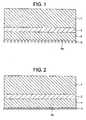
- FIG. 2 shows an ultra-thin copper foil with a carrier foil of the first embodiment of the present invention
- a peeling layer 2 is formed on the surface of a carrier foil 1
- an ultra-thin copper foil 4 is formed on the peeling layer 2.
- the ultra-thin copper foil with a carrier foil of the first embodiment of the present invention is constituted by laminating the carrier foil 1, the peeling layer 2 and the ultra-thin copper foil 4.
- the surface roughness Rz of the surface of the ultra-thin copper foil 4 is 2.5 ⁇ m or less and the minimum distance between peaks of salients of a based material is 5 ⁇ m or more, and a roughening grain layer 5 consisting of roughening grains 4a is formed on the surface.
- plating is formed by a copper plating solution that can generate a smooth surface and mirror gloss.
- the copper plating solution that can generate a smooth surface and mirror gloss, it is optimal that the copper plating solution disclose in Japanese Patent No. 3313277 or the solution containing a commercially available gloss plating dopant for decoration is used.
- the ultra-thin copper foil 4 obtained from these plating solution has small surface roughness, and has a flat surface condition, further crystal grains having average grain diameter of 2 ⁇ m are deposited, even in the case that a copper roughening grains are deposited, to form evenly microscopic grains having average grain diameter of 2 ⁇ m as illustrated as a small points in FIG. 2.
- the average grain diameter of the crystal grain of the foil itself is the calculated value that first, a picture of the surface that the crystal grains are formed is taken by a transmission electron microscope (TEM), the area of the crystal grain in the picture is measured over ten point and the diameter is calculated when the crystal grain is defined as a perfect circle.
- TEM transmission electron microscope
- the average grain diameter of the microscopic grains is an average value that is measured actually in SEM and is measured over ten points.
- the peeling layer 2 set on the carrier foil 1 consists of Cr, Ni, Co, Fe, Mo, Ti, W, P and/or these alloy layer or these hydrous oxide layer, or an organic film.
- these metals including alloy metal
- those hydrous oxides forming the peeling layer 2 are formed by cathodic electrolytic treatment. Note that in a stage that wiring board that the ultra-thin copper foil with a carrier foil is used is formed, for stabilizing the peeling after laminating the ultra-thin copper foil with a carrier foil on the insulating substrate, nickel, iron or these alloy layer may be set together under the peeling layer 2.
- nickel-chromium, cobalt-chromium, chromium-tungsten, chromium-copper, chromium-iron, chromium-titanium nickel-chromium, cobalt-chromium, chromium-tungsten, chromium-copper, chromium-iron, chromium-titanium
- nickel-iron-chromium, nickel-chromium-molybdenum, nickel-chromium-tungsten, nickel-chromium-copper, nickel-chromium-phosphorus, cobalt-iron-chromium, cobalt-chromium-molybdenum, cobalt-chromium-tungsten, cobalt-chromium-copper, cobalt-chromium-phosphorus, etc. can be mentioned.
- an organic film for the peeling layer 2 it is preferable that a thing consisting of one kind or two kind or more selected from among an organic compound including nitrogen, an organic compound including sulfur or a carboxylic acid is used.
- the peel strength at the time of peeling the carrier foil 1 from the peeling layer 2 is influenced with the amount of deposition of these metals. That is, if an peeling layer 2 is thick (that is, if there is the large amount of deposition of plated metal), the surface of the carrier foil 1 is covered with the metal constituting the peeling material (hereinafter called as peeling layer metal) completely, it is considered that the peel strength corresponds to the peeling power which tears off the joint surfaces between the surface of the peeling layer metal and the ultra-thin copper foil 4 stacked afterward.
- the peel strength is the peeling power which tears off the joint surfaces between the carrier foil 1 which is exposed slightly and the peeling layer metal and the ultra-thin copper foil 4 deposited on them.
- the peel strength of the carrier foil 1 and the ultra-thin copper foil 4 changes with the amount of deposition of plated metal that forms a peeling layer 2, however, since if a peeling layer 2 is formed (deposited) to some extent thickly, the peel strength will not change any more, even if the amount of deposition of the metal which forms a peeling layer 2 is made 100 mg/dm 2 or more, the peel strength does not change.
- An untreated electrolytic copper foil having the surface (S surface) roughness of 1.2 ⁇ m and the thickness of 35 ⁇ m was defined as a carrier foil and on the S surface chromium electroplating was successively performed, a chromium plating layer (peeling layer) of the thickness of 0.005 pm was formed.
- a chromium plating layer peeling layer of the thickness of 0.005 pm was formed.
- Ni 0.1 mg/dm 2
- Zn 0.1 mg/dm 2
- An untreated electrolytic copper foil having the surface (S surface) roughness of 1.2 ⁇ m and the thickness of 35 ⁇ m was defined as a carrier foil and on the S surface chromium electroplating was successively performed, a chromium plating layer (peeling layer) of the thickness of 0.005 ⁇ m was formed.
- a chromium plating layer peeling layer of the thickness of 0.005 ⁇ m was formed.
- an ultra-thin copper layer (copper foil) having the thickness of 5 ⁇ m was electroplated.
- composition 2 copper sulfate (CuSO 4 ⁇ 5H 2 O) 240 g/l sulfuric acid (H 2 SO 4 ) 60 g/l cupracid 210 by Nihon Schering K.K. make up agent 0.5 cc/l brightening agent (A) 0.5 cc/l brightening agent (B) Cl - using for only complement 30 ppm Note that as the complement of the brightening agent, the brightening agent (A) and the brightening agent (B) were added 300 cc respectively for amount of the current of 1000 Ah.
- Example 2 On the ultra-thin copper foil that obtained copper grains were deposited, the treatment similar to Example 1 was preformed.
- An untreated electrolytic copper foil having the surface (S surface) roughness of 1.8 ⁇ m and the thickness of 35 ⁇ m was defined as a carrier foil and on the S surface in a way similar to Example 1, a peeling layer, an ultra-thin copper foil, a roughening grain layer were formed, and next, surface treatment was performed to produce an ultra-thin copper foil with a carrier foil.
- An untreated electrolytic copper foil having the surface (S surface) roughness of 1.8 ⁇ m and the thickness of 35 ⁇ m was defined as a carrier foil and on the S surface in a way similar to Example 2, a peeling layer, an ultra-thin copper foil, a roughening grain layer were formed, and next, surface treatment was performed to produce an ultra-thin copper foil with a carrier foil.
- An untreated electrolytic copper foil having the surface (S surface) roughness of 2.4 ⁇ m and the thickness of 35 ⁇ m was defined as a carrier foil and on the S surface in a way similar to Example 1, a peeling layer, an ultra-thin copper foil, a roughening grain layer were formed, and next, surface treatment was performed to produce an ultra-thin copper foil with a carrier foil.
- An untreated electrolytic copper foil having the surface (S surface) roughness of 2.4 ⁇ m and the thickness of 35 ⁇ m was defined as a carrier foil and on the S surface in a way similar to Example 2, a peeling layer, an ultra-thin copper foil, a roughening grain layer were formed, and next, surface treatment was performed to produce an ultra-thin copper foil with a carrier foil.
- An untreated electrolytic copper foil having the surface (S surface) roughness of 1.2 pm and the thickness of 35 ⁇ m was defined as a carrier foil and on the S surface chromium electroplating was successively performed, a chromium plating layer (peeling layer) of the thickness of 0.005 ⁇ m was formed.
- a chromium plating layer peeling layer of the thickness of 0.005 ⁇ m was formed.
- an ultra-thin copper layer (copper foil) having the thickness of 5 ⁇ m was electroplated.
- composition 3 copper sulfate (CuSO 4 ⁇ 5H 2 O) 250 g/l to 350 g/l sulfuric acid (H 2 SO 4 ) 80 g/l to 120 g/l low-molecular-weight glue 1 ppm to 10 ppm Cl - 10 ppm to 50 ppm
- capsule plating was electrodeposited.
- An untreated electrolytic copper foil having the surface (S surface) roughness of 1.8 ⁇ m and the thickness of 35 ⁇ m was defined as a carrier foil and on the S surface in a way similar to Comparative example 1, a peeling layer, an ultra-thin copper foil, a roughening grain layer were formed, and next surface treatment was performed to produce an ultra-thin copper foil with a carrier foil.
- An untreated electrolytic copper foil having the surface (S surface) roughness of 2.4 ⁇ m and the thickness of 35 ⁇ m was defined as a carrier foil and on the S surface in a way similar to Comparative example 1, a peeling layer, an ultra-thin copper foil, a roughening grain layer were formed, and next surface treatment was performed to produce an ultra-thin copper foil with a carrier foil.
- a rolled copper foil having the surface roughness of 0.6 ⁇ m and the thickness of 35 ⁇ m was defined as a carrier foil and on the surface in a way similar to Comparative example 1, a peeling layer, an ultra-thin copper foil, a roughening grain layer were formed, and next surface treatment was performed to produce an ultra-thin copper foil with a carrier foil.
- An untreated electrolytic copper foil having the thickness of 35 ⁇ m was formed by using electrolytic solution having composition disclosed in Published Japanese translation of a PCT application No. 2003-524078 as a carrier foil.
- electrolytic solution having composition disclosed in Published Japanese translation of a PCT application No. 2003-524078 as a carrier foil.
- a peeling layer, an ultra-thin copper foil, a roughening grain layer were formed, and next surface treatment was performed to produce an ultra-thin copper foil with a carrier foil.
- the ultra-thin copper foil with a carrier foil of the present invention even electrodeposition property of copper plating is superior, and as is clear from Table. 1, by performing copper plating of the thickness of 5 ⁇ m, even if the surface roughness of former foil is as rough as 2.4 ⁇ m, the surface roughness of the surface of the ultra-thin copper foil becomes small, the surface roughness after performing the roughening treatment is controlled small.
- the peel strength of the ultra-thin copper foil with a carrier foil produced in examples 1 to 6 and Comparative examples 1 to 5 was measured.
- the ultra-thin copper foil with a carrier foil defined as width of 10 mm was bonded on FR-4 substrate, next the carrier foil was peeled, and after plating was performed on the ultra-thin copper foil to be the thickness of 35 ⁇ m, it was peeled to measure the peel strength.
- the result was indicated together in Table. 1.
- Table. 1 in the usual measure method (width of 10 mm), the peel strength in Comparative examples is larger than in Examples.
- the peel strength in Comparative examples is larger, because since salients and depressions exist on the surface of copper foil before roughening, roughening grains are focusing to a salient portion to electrodeposit, and in a depression portion roughening grains are not electrodeposited but since the measurement is used wide width as 100 mm the anchoring effect of the roughening grains occurs to be large peel strength. However, when width becomes to be ultra-fine width such as 50 ⁇ m or less, the peel strength is reduced so as indicating below.
- the 5 ⁇ m foil with a carrier foil of Examples 1 to 6 and Comparative examples 1 to 5 was pressed on FR-4 substrate and the carrier was peeled off.
- the line width in the case that ten lines could be etched without bridging was indicated numerically in Table. 1. Etching was possible until 15 pm or less in the ultra-thin copper foil produced in Examples, on the contrary, the lowest value of the ultra-thin copper foil produced in Comparative examples was 20 ⁇ m.
- an ultra-thin copper foil with a carrier foil of the first embodiment of the present invention has excellent effects such that an ultra-thin copper electrolytic foil with a carrier foil that microscopic crystal grains are deposited without being affected by the surface roughness of the carrier foil can be produced, even after depositing roughening grains on the foil Rz can be controlled within 2 ⁇ m to 3 ⁇ m, etching can be performed until ultra-fine width such that line/space is 15 pm or less, and, even after etching lines of 15 ⁇ m or less, since a large number of roughening grains are deposited in the line of 15 pm or less, despite roughness is low, fine lines and wiring board (resin substrate) have adhesive strength, and adhesive strength is large. Therefore, a printed wiring board having high density ultra-fine wiring (ultra-fine pattern) and a multilayer printed wiring board having ultra-fine pattern can be provided.
- An ultra-thin copper foil of the present invention is possible to etch until ultra-fine such that line width is 15 ⁇ m or less, and has large peel strength, hence that may not peel from a wiring substrate.
- a copper foil of the present invention can be applied to a circuit conductor of various kinds of wiring device, printed wiring board can be applied to various kinds of electronics device.
- FIG. 3 and FIG. 4 are showing an ultra-thin copper foil with a carrier foil of the second embodiment of the present invention, a peeling layer 2 and an ultra-thin copper foil 4 are electroplated and formed on the surface of a carrier foil 1.
- Roughening treatment is not performed on the surface of the ultra-thin copper foil 4, however, chemical treatment and/or electrochemical treatment (that is not illustrated) at a degree that the surface profile may not be changed are performed. By this treatment, chemical bond with a resin substrate and peel strength are improved.
- plating is performed by the copper plating solution not including dopant or the copper plating solution including dopant.
- the dopant means inorganic compound dopant such as arsenic compound, molybdenum compound, vanadium compound, nickel compound, cobalt compound, iron compound, tungsten compound, germanium compound and so on, or organic compound dopant such as glue, gelatin, organic active sulfur containing compound, organic dye, polymer polysaccharide, cellulose and so on.
- the shape of the surface of the ultra-thin copper foil 4 becomes a shape such that salients lie in a row (this is called as "salient of a based material").
- Rz indicates ten point height of roughness profile described in Japanese Industrial Standards (JIS) B 0601-1994.
- the copper foil becomes more suitable for forming fine pattern.
- Rz of the surface of ultra-thin copper foil 4 formed from copper plating solution not containing component except for copper as major component, that is to say, not containing inorganic and organic dopant can be made about 1 ⁇ m to 2 ⁇ m and the minimum distance between peaks can be made 5 ⁇ m or more by selecting current density and flow velocity of the electrolytic solution (state of stirring) at the time of producing foils.
- the surface of the ultra-thin copper foil 4 is a surface shape that a number of small salients and depressions exist, when producing a printed wiring board by using this ultra-thin copper foil with a carrier foil peel strength with a resin substrate is excellent and fine wiring can be formed.
- roughening grain does not exist and organic or inorganic impurities included in the layer of the ultra-thin copper foil 4 are very few, when wiring is etched, the fine wiring can be formed.
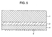
- FIG. 5 is showing an ultra-thin copper foil with a carrier foil of the third embodiment, and showing a example that treatment of making unevenness is performed on the surface of an ultra-thin copper foil 4 by chemical etching, and/or treatment of making unevenness are performed by electrochemical etching.
- a peeling layer 2 and the ultra-thin copper foil 4 are laminated and formed on the surface of a carrier foil 1.
- a small tip 6 is formed on the surface of the ultra-thin copper foil 4. Further, chemical treatment and/or electrochemical treatment (that is not illustrated) by the thickness at a degree that the surface profile on the surface of the ultra-thin copper foil 4 is not changed are performed.
- the peeling layer 2 set on the carrier foil 1 is a layer consisting of Cr, Ni, Co, Fe, Mo, Ti, W, P and/or these alloy layer or these hydrous oxide layer, or is an organic film.
- these metals including alloy metal
- those hydrous oxides forming these peeling layers are formed by cathodic electrolytic treatment. Note that in a stage that wiring board that the ultra-thin copper foil with a carrier foil is used is formed, for stabilizing the peeling after laminating the ultra-thin copper foil with a carrier foil on the insulating substrate, nickel, iron or these alloy layer may be set together under these peeling layers.
- Preferable binary alloy of chromium alloy for the peeling layer 2 means nickel-chromium, cobalt-chromium, chromium-tungsten, chromium-copper, chromium-iron, chromium-titanium.
- the ternary alloy means nickel-iron-chromium, nickel-chromium-molybdenum, nickel-chromium-tungsten, nickel-chromium-copper, nickel-chromium-phosphorus, cobalt-iron-chromium, cobalt-chromium-molybdenum, cobalt-chromium-tungsten, cobalt-chromium-copper, cobalt-chromium-phosphorus, etc.
- an organic film for the peeling layer 2 it is preferable that a thing consisting of one kind or two kind or more selected from among an organic compound including nitrogen, an organic compound including sulfur or a carboxylic acid is used.
- the peel strength at the time of peeling the carrier foil 1 from the peeling layer 2 is influenced with the amount of deposition of these metals. That is, if an peeling layer is thick (that is, if there is the large amount of deposition of plated metal), the surface of the carrier foil is covered with the metal constituting the peeling layer (hereinafter called as peeling layer metal) completely, it is considered that the peel strength corresponds to the peeling power which tears off the joint surfaces between the surface of the peeling layer metal and the ultra-thin copper foil stacked afterward.
- the peel strength is the peeling power which tears off the joint surfaces between the carrier foil which is exposed slightly and the peeling layer metal and the ultra-thin copper foil deposited on them. Therefore, although the peel strength of the carrier foil and the ultra-thin copper foil changes with the amount of deposition of plated metal that forms a peeling layer, if a peeling layer is formed (deposited) to some extent thickly, the peel strength will not change any more. According to the experiment, as the amount of deposition of the metal, which forms a peeling layer, even if the amount of deposition of is made 100 mg/dm 2 or more, the peel strength does not change.
- An untreated electrolytic copper foil having the surface (S surface) roughness of 1.8 ⁇ m and the thickness of 35 ⁇ m was defined as a carrier foil and on the S surface chromium electroplating was successively performed, a chromium plating layer (peeling layer) of the thickness of 0.005 ⁇ m was formed.
- a copper sulfate solution described in the following composition 4 was used as an electrolytic solution and the electrolysis was performed in a condition that the current density was 10 A/dm 2 to 30 A/dm 2 and the temperature of the solution was 40 degrees C to 60 degrees C, an ultra-thin copper layer (copper foil) having the thickness of 5 ⁇ m was electroplated.
- Condition of copper pyrophosphate strike plating Cu 2 P 2 O 7 ⁇ 3H 2 O 5 g/l to 50 g/l K 4 P 2 O 7 50 g/l to 300 g/l pH 8 to 10 current density 1 A/dm 2 to 3 A/dm 2 treatment time 30 seconds (Composition 4) copper sulfate (CuSO 4 ⁇ 5H 2 O) 250 g/l to 350 g/l sulfuric acid (H 2 SO 4 ) 80 g/l to 120 g/l
- Ni 0.1 mg/dm 2
- An untreated electrolytic copper foil having the surface (S surface) roughness of 1.8 ⁇ m and the thickness of 35 ⁇ m was defined as a carrier foil and on the S surface chromium electroplating was successively performed, a chromium plating layer (peeling layer) of the thickness of 0.005 ⁇ m was formed.
- a copper sulfate solution described in the following composition 5 was used as an electrolytic solution and the electrolysis was performed in a condition that the current density was 10 A/dm 2 to 30 A/dm 2 and the temperature of the solution was 50 degrees C, an ultra-thin copper layer (copper foil) having the thickness of 5 ⁇ m was electroplated.
- composition 5 copper sulfate (CuSO 4 ⁇ 5H 2 O) 250 g/l to 350 g/l sulfuric acid (H 2 SO 4 ) 80 g/l to 120 g/l glue 1 ppm to 10 ppm Cl - 10 ppm to 50 ppm
- An untreated electrolytic copper foil having the surface (S surface) roughness of 1.8 ⁇ m and the thickness of 35 ⁇ m was defined as a carrier foil and on the S surface chromium electroplating was successively performed, a chromium plating layer (peeling layer) of the thickness of 0.005 ⁇ m was formed.
- a copper sulfate solution described in the following composition 6 was used as an electrolytic solution and the electrolysis was performed in a condition that the current density was 10 A/dm 2 to 30 A/dm 2 and the temperature of the solution was 50 degrees C, an ultra-thin copper layer (copper foil) having the thickness of 5 ⁇ m was electroplated.
- composition 6 copper sulfate (CuSO 4 ⁇ 5H 2 O) 250 g/l to 350 g/l sulfuric acid (H 2 SO 4 ) 80 g/l to 120 g/l 3-mercapto-1-sodium propanesulfonate 0.5 ppm to 5 ppm hydroxyethyl cellulose 1 ppm to 10 ppm low-molecular-weight glue (molecular weight 3000) 1 ppm to 10 ppm Cl - 10 ppm to 50 ppm
- An untreated electrolytic copper foil having the surface (S surface) roughness of 1.8 ⁇ m and the thickness of 35 ⁇ m was defined as a carrier foil, after performing electroplating of chromium on the S surface and strike-plating by copper pyrophosphate plating solution, ultra-thin copper layer (copper foil) having the thickness of 6 ⁇ m was electroplated.
- the surface was etched by 1 ⁇ m by etchBOND of MEC CO.,LTD.
- the etching condition is indicated below.
- treatment chemical cz-8100 spray pressure 2.0 kg/cm 2 treatment temperature 35 degrees C
- An untreated electrolytic copper foil having the surface (S surface) roughness of 1.8 ⁇ m and the thickness of 35 ⁇ m was defined as a carrier foil, after performing electroplating of chromium on the S surface and strike-plating by copper pyrophosphate plating solution, ultra-thin copper layer (copper foil) having the thickness of 7 ⁇ m was electroplated.
- Theoretical dissolution quantity is 2 ⁇ m.
- the theoretical amount of dissolution means the dissolution quantity calculated from the applied electric quantity in the case of dissolving in a state that electric efficiency is 100 percent.
- composition of electrolytic solution hydrochloric acid (HCL) 80 g/l to 100 g/l
- temperature of electrolytic solution 40 degrees C
- current density 25 A/dm 2 to 40 A/dm 2
- treatment time 12.5 seconds to 25 seconds
- An untreated electrolytic copper foil having the surface (S surface) roughness of 1.8 ⁇ m and the thickness of 35 ⁇ m was defined as a carrier foil, after performing electroplating of chromium on the S surface and strike-plating by copper pyrophosphate plating solution, ultra-thin copper layer (copper foil) having the thickness of 5 ⁇ m was electroplated.
- Cathodic electrolytic treatment was performed by direct current and microscopic roughening copper grains are electrodeposited on the ultra-thin copper foil in the following condition.
- composition of electrolytic solution copper sulfate (CuSO 4 ⁇ 5H 2 O) 90 g/l to 130 g/l sulfuric acid (H 2 SO 4 ) 110 g/l to 140 g/l arsenious acid (As 2 O 3 ) 100 ppm to 200 ppm (as As)
- temperature of electrolytic solution 30 degrees C
- current density 10 A/dm 2 to 50 A/dm 2
- treatment time 2 seconds to 15 seconds
- composition of electrolytic solution copper sulfate (CuSO 4 ⁇ 5H 2 O) 200 g/l to 300 g/l sulfuric acid (H 2 SO 4 ) 90 g/l to 130 g/l
- temperature of electrolytic solution 50 degrees C
- current density 10 A/dm 2 to 30 A/dm 2
- treatment time 2 seconds to 15 seconds
- An untreated electrolytic copper foil having the surface (S surface) roughness of 1.8 ⁇ m and the thickness of 35 ⁇ m was defined as a carrier foil, after performing electroplating of chromium on the S surface and strike-plating by copper pyrophosphate plating solution, ultra-thin copper layer (copper foil) having the thickness of 5 ⁇ m was electroplated.
- Cathodic electrolytic treatment was performed by direct current and microscopic roughening copper grains are electrodeposited on the ultra-thin copper foil in the condition equal to Comparative example 6.
- An untreated electrolytic copper foil having the surface (S surface) roughness of 1.8 ⁇ m and the thickness of 35 ⁇ m was defined as a carrier foil, after performing electroplating of chromium on the S surface and strike-plating by copper pyrophosphate plating solution, ultra-thin copper layer (copper foil) having the thickness of 5 ⁇ m was electroplated.
- Cathodic electrolytic treatment was performed by direct current and microscopic roughening copper grains are electrodeposited on the ultra-thin copper foil in the condition equal to Comparative example 6.
- Example 7 For each ultra-thin copper foil produced in Example 7 to 12, Comparative examples 6 to 8, the surface roughness (ten point height of roughness profile) Rz of the ultra-thin copper foil was measured, and the result was indicated in Table. 2.
- Carrier foil Roughness of S surface (Rz: ⁇ m) Copper plating solution
- Surface roughness after roughening treatment (Rz: ⁇ m) Peel strength (kN/cm) Etching property (L/S: ⁇ m)
- Example 7 35 ⁇ m MP foil 1.8 composition 1 1.9 1.9 1.00 10/10
- Example 8 35 ⁇ m MP foil 1.8 composition 2 2.1 2.1 1.05 10/10
- Example 9 35 ⁇ m MP foil 1.8 composition 3 1.7 1.7 0.80 10/10
- Example 10 35 ⁇ m MP foil 1.8 composition 1 1.9 2.5 1.10 10/10
- Example 11 35 ⁇ m MP foil 1.8 composition 1 1.9 1.9 1.15 10/10
- Example 12 35 ⁇ m MP foil 1.8 composition 1
- the peel strength of the ultra-thin copper foil with a carrier foil produced in examples 7 to 12 and Comparative examples 6 to 8 was measured.
- a polyimide sheet (UPILEX-VT made by Ube Industry) was placed on the surface of the ultra-thin copper foil, the assembly was sandwiched with two flat stainless steel plates, then the assembly was laminated at the temperature of 330 degrees C and the pressure of 2 kg/cm 2 for 10 minutes by 20 torr vacuum press, then was laminated at the temperature of 330 degrees C and the pressure of 50 kg/cm 2 for 5 minutes to produce a one-sided copper-clad polyimide laminated board for the test of peel strength with a carrier foil.
- the peel strength was measured by 10 mm width. The result is indicated together in Table. 2.
- the carrier foil was peeled.
- the line width in the case that ten lines could be etched without bridging was indicated numerically in Table. 2. Etching was possible until 10 ⁇ m or less in the ultra-thin copper foil produced in Examples, on the contrary, the minimum of the ultra-thin copper foil produced in Comparative examples was 30 ⁇ m.
- chemical treatment and/or electrochemical treatment for improving peel strength with a resin substrate was performed without depositing roughening grains that etching speed is low on the ultra-thin copper foil with a carrier foil by the second and third embodiments of the present invention, or after performing treatment of making unevenness by chemical etching and/or eleotrochemical etching without depositing roughening grains that etching speed is low on the ultra-thin copper foil, further chemical treatment and/or electrochemical treatment for improving peel strength with a resin substrate was performed.
Landscapes
- Engineering & Computer Science (AREA)
- Chemical & Material Sciences (AREA)
- Chemical Kinetics & Catalysis (AREA)
- Electrochemistry (AREA)
- Materials Engineering (AREA)
- Metallurgy (AREA)
- Organic Chemistry (AREA)
- Microelectronics & Electronic Packaging (AREA)
- Manufacturing & Machinery (AREA)
- Electroplating Methods And Accessories (AREA)
- Parts Printed On Printed Circuit Boards (AREA)
- Laminated Bodies (AREA)
Applications Claiming Priority (4)
| Application Number | Priority Date | Filing Date | Title |
|---|---|---|---|
| JP2003381399 | 2003-11-11 | ||
| JP2003381399 | 2003-11-11 | ||
| JP2004070806 | 2004-03-12 | ||
| JP2004070806A JP4217786B2 (ja) | 2004-03-12 | 2004-03-12 | キャリア付き極薄銅箔、およびキャリア付き極薄銅箔を用いた配線板 |
Publications (2)
| Publication Number | Publication Date |
|---|---|
| EP1531656A2 true EP1531656A2 (de) | 2005-05-18 |
| EP1531656A3 EP1531656A3 (de) | 2007-10-03 |
Family
ID=34436975
Family Applications (1)
| Application Number | Title | Priority Date | Filing Date |
|---|---|---|---|
| EP04026739A Ceased EP1531656A3 (de) | 2003-11-11 | 2004-11-10 | Ultradünne Kupferfolie mit Träger und Leiterplatte unter Verwendung einer ultradünnen Kupferfolie mit Träger |
Country Status (5)
| Country | Link |
|---|---|
| US (2) | US20050158574A1 (de) |
| EP (1) | EP1531656A3 (de) |
| KR (1) | KR101108991B1 (de) |
| CN (1) | CN100571483C (de) |
| TW (1) | TW200533261A (de) |
Cited By (6)
| Publication number | Priority date | Publication date | Assignee | Title |
|---|---|---|---|---|
| EP1802183A3 (de) * | 2005-12-15 | 2008-01-23 | Furukawa Circuit Foil Co., Ltd. | Ultradünne Kupferfolie mit Träger und Leiterplatte und dessen Verwendung |
| DE102008022722A1 (de) * | 2008-05-06 | 2009-11-12 | Siemens Aktiengesellschaft | Verfahren zum elektrochemischen Erzeugen eines Metallbandes |
| US7892655B2 (en) | 2005-12-15 | 2011-02-22 | The Furukawa Electric Co., Ltd. | Ultrathin copper foil with carrier and printed circuit board using same |
| EP3072682A1 (de) * | 2012-03-26 | 2016-09-28 | JX Nippon Mining & Metals Corporation | Leiterplatte und verfahren zur deren herstellung |
| CN109234797A (zh) * | 2018-11-02 | 2019-01-18 | 山东天岳先进材料科技有限公司 | 一种碳化硅单晶生长装置 |
| EP4105365A1 (de) * | 2021-06-18 | 2022-12-21 | Dongguan DSP Technology Co., Ltd. | Verfahren zur oberflächenbehandlung von kupfer für die verbindung von polymer und kupfer |
Families Citing this family (59)
| Publication number | Priority date | Publication date | Assignee | Title |
|---|---|---|---|---|
| WO2006013950A1 (ja) * | 2004-08-05 | 2006-02-09 | Kaneka Corporation | 溶液、めっき用材料、絶縁シート、積層体及びプリント配線板 |
| WO2006041117A1 (ja) * | 2004-10-14 | 2006-04-20 | Kaneka Corporation | めっき用材料、該めっき用材料に用いるポリアミド酸溶液、ポリイミド樹脂溶液、及びこれらを用いてなるプリント配線板 |
| CN1984526B (zh) * | 2005-12-15 | 2011-01-12 | 古河电气工业株式会社 | 带载体的极薄铜箔及印刷电路基板 |
| US20080142249A1 (en) * | 2006-12-13 | 2008-06-19 | International Business Machines Corporation | Selective surface roughness for high speed signaling |
| JP5335893B2 (ja) * | 2008-04-14 | 2013-11-06 | ヨーロピアン オーガナイゼーション フォー ニュークリア リサーチ | ガス電子増倍管の製造方法 |
| EP2351876A1 (de) | 2008-11-25 | 2011-08-03 | JX Nippon Mining & Metals Corporation | Kupferfolie für leiterplatten |
| US20110233320A1 (en) * | 2008-11-25 | 2011-09-29 | Jx Nippon Mining & Metals Corporation | Method of winding up copper foil or copper clad laminate |
| JP2009143234A (ja) | 2008-12-24 | 2009-07-02 | Nippon Mining & Metals Co Ltd | キャリア付金属箔 |
| CN102264538A (zh) | 2008-12-26 | 2011-11-30 | 吉坤日矿日石金属株式会社 | 柔性层压板以及使用该层压板形成的柔性电子电路基板 |
| JP5505828B2 (ja) * | 2009-03-04 | 2014-05-28 | 福田金属箔粉工業株式会社 | 複合金属箔及びその製造方法 |
| KR101298999B1 (ko) * | 2009-09-01 | 2013-08-23 | 일진머티리얼즈 주식회사 | 미세회로 형성을 위한 임베디드용 동박 |
| JP5885054B2 (ja) * | 2010-04-06 | 2016-03-15 | 福田金属箔粉工業株式会社 | 銅張積層板用処理銅箔及び該処理銅箔を絶縁性樹脂基材に接着してなる銅張積層板並びに該銅張積層板を用いたプリント配線板。 |
| TWI411707B (zh) * | 2010-04-22 | 2013-10-11 | Nanya Plastics Corp | Ultra - low copper foil as the carrier of ultra - thin copper foil and its use |
| CN103154327A (zh) * | 2010-10-06 | 2013-06-12 | 古河电气工业株式会社 | 铜箔及其制备方法、带有载体的铜箔及其制备方法、印刷电路板、多层印刷电路板 |
| CN102452197B (zh) | 2010-10-21 | 2014-08-20 | 财团法人工业技术研究院 | 附载箔铜箔及其制造方法 |
| TWI405510B (zh) * | 2010-11-24 | 2013-08-11 | Co Tech Copper Foil Coporation | 經粗化處理的銅箔及其製造方法 |
| JP5651564B2 (ja) * | 2011-09-30 | 2015-01-14 | 富士フイルム株式会社 | 貼り付け用銅箔 |
| JP5875350B2 (ja) * | 2011-11-30 | 2016-03-02 | 三井金属鉱業株式会社 | 電解銅合金箔及びキャリア箔付電解銅合金箔 |
| WO2014051122A1 (ja) * | 2012-09-28 | 2014-04-03 | Jx日鉱日石金属株式会社 | キャリア付金属箔 |
| CN103060882B (zh) * | 2013-01-21 | 2015-11-04 | 福建清景铜箔有限公司 | 一种硫酸铜溶液逆向流动生产电解铜箔的方法及系统 |
| KR101540151B1 (ko) * | 2013-06-18 | 2015-07-28 | 삼성전기주식회사 | 인쇄회로기판의 제조방법 |
| TWI533496B (zh) * | 2013-07-23 | 2016-05-11 | Chang Chun Petrochemical Co | Electrolytic copper foil |
| JP2015028197A (ja) * | 2013-07-30 | 2015-02-12 | 株式会社Shカッパープロダクツ | 粗化銅箔、銅張積層板及びプリント配線板 |
| TWI589201B (zh) * | 2013-11-22 | 2017-06-21 | Mitsui Mining & Smelting Co | Manufacturing method of a printed circuit board having a buried circuit and a printed circuit board obtained by the manufacturing method |
| JP5870148B2 (ja) * | 2013-11-27 | 2016-02-24 | Jx金属株式会社 | キャリア付銅箔、プリント回路板の製造方法、銅張積層板、銅張積層板の製造方法、及び、プリント配線板の製造方法 |
| JP2015134953A (ja) * | 2014-01-17 | 2015-07-27 | Jx日鉱日石金属株式会社 | 表面処理銅箔、キャリア付銅箔、プリント配線板、プリント回路板、銅張積層板及びプリント配線板の製造方法 |
| TWI639515B (zh) * | 2014-03-21 | 2018-11-01 | Jx日鑛日石金屬股份有限公司 | 附載子金屬箔 |
| JP6640567B2 (ja) | 2015-01-16 | 2020-02-05 | Jx金属株式会社 | キャリア付銅箔、積層体、プリント配線板、電子機器の製造方法及びプリント配線板の製造方法 |
| KR102031065B1 (ko) * | 2015-01-22 | 2019-10-11 | 미쓰이금속광업주식회사 | 캐리어 부착 극박 동박 및 그 제조 방법, 동장 적층판, 및 프린트 배선판의 제조 방법 |
| CN105843438A (zh) * | 2015-01-30 | 2016-08-10 | 启耀光电股份有限公司 | 电子装置及电子装置的制造方法 |
| JP6782561B2 (ja) | 2015-07-16 | 2020-11-11 | Jx金属株式会社 | キャリア付銅箔、積層体、積層体の製造方法、プリント配線板の製造方法及び電子機器の製造方法 |
| JP6006445B1 (ja) | 2015-07-27 | 2016-10-12 | Jx金属株式会社 | キャリア付銅箔、積層体、プリント配線板の製造方法及び電子機器の製造方法 |
| JP6058182B1 (ja) | 2015-07-27 | 2017-01-11 | Jx金属株式会社 | キャリア付銅箔、積層体、プリント配線板の製造方法及び電子機器の製造方法 |
| JP6200042B2 (ja) | 2015-08-06 | 2017-09-20 | Jx金属株式会社 | キャリア付銅箔、積層体、プリント配線板の製造方法及び電子機器の製造方法 |
| JP6190500B2 (ja) | 2015-08-06 | 2017-08-30 | Jx金属株式会社 | キャリア付銅箔、積層体、プリント配線板の製造方法及び電子機器の製造方法 |
| JP6339636B2 (ja) | 2015-08-06 | 2018-06-06 | Jx金属株式会社 | キャリア付銅箔、積層体、プリント配線板の製造方法及び電子機器の製造方法 |
| WO2018003703A1 (ja) * | 2016-07-01 | 2018-01-04 | 三菱瓦斯化学株式会社 | 半導体素子搭載用パッケージ基板の製造方法及び半導体素子実装基板の製造方法 |
| CN109642338B (zh) * | 2016-09-12 | 2021-02-09 | 古河电气工业株式会社 | 铜箔以及具有该铜箔的覆铜板 |
| KR101809985B1 (ko) * | 2017-03-30 | 2017-12-18 | 와이엠티 주식회사 | 다공성 구리박의 제조방법 및 이를 이용한 다공성 구리박 |
| WO2018181726A1 (ja) * | 2017-03-30 | 2018-10-04 | 古河電気工業株式会社 | 表面処理銅箔、並びにこれを用いた銅張積層板およびプリント配線板 |
| KR101992841B1 (ko) | 2017-07-13 | 2019-06-27 | 케이씨에프테크놀로지스 주식회사 | 울음, 주름 및 찢김이 최소화된 동박, 그것을 포함하는 전극, 그것을 포함하는 이차전지, 및 그것의 제조 방법 |
| KR102353143B1 (ko) * | 2017-07-24 | 2022-01-18 | 후루카와 덴키 고교 가부시키가이샤 | 표면 처리 동박, 그리고 이것을 이용한 동 클래드 적층판 및 프린트 배선판 |
| JP2020508231A (ja) * | 2017-07-31 | 2020-03-19 | サーキット フォイル ルクセンブルグ エス.エイ.アール.エル.Circuit Foil Luxembourg S.A.R.L. | 銅張積層基板およびこれを含む印刷回路基板 |
| KR102390417B1 (ko) * | 2017-12-05 | 2022-04-22 | 후루카와 덴키 고교 가부시키가이샤 | 표면 처리 동박, 그리고 이것을 이용한 동 클래드 적층판 및 프린트 배선판 |
| JP7014695B2 (ja) * | 2018-10-18 | 2022-02-01 | Jx金属株式会社 | 導電性材料、成型品及び電子部品 |
| KR102124324B1 (ko) | 2018-11-14 | 2020-06-18 | 와이엠티 주식회사 | 도금 적층체 및 인쇄회로기판 |
| CN111640915B (zh) | 2019-03-01 | 2024-12-31 | 麻省固能控股有限公司 | 负极、包括其的二次电池以及制造负极的方法 |
| US11444277B2 (en) | 2019-03-01 | 2022-09-13 | Ses Holdings Pte. Ltd. | Anodes, secondary batteries including the same, and methods of making anodes |
| WO2020246467A1 (ja) * | 2019-06-07 | 2020-12-10 | 古河電気工業株式会社 | 表面処理銅箔、銅張積層板、及びプリント配線板 |
| TWI719698B (zh) * | 2019-06-12 | 2021-02-21 | 金居開發股份有限公司 | 進階反轉電解銅箔及其銅箔基板 |
| CN110996536B (zh) * | 2019-12-25 | 2023-06-02 | 广东生益科技股份有限公司 | 一种载体铜箔及其制备方法和应用 |
| CN112469194B (zh) * | 2020-11-27 | 2022-08-05 | 广东嘉元科技股份有限公司 | 一种高密互联电路板用低轮廓电解铜箔 |
| KR102686711B1 (ko) * | 2020-12-10 | 2024-07-19 | 와이엠티 주식회사 | 캐리어 부착 금속박용 이형층 및 이를 포함하는 금속박 |
| TWI796042B (zh) * | 2020-12-10 | 2023-03-11 | 韓商Ymt股份有限公司 | 用於具有載體的金屬箔的離型層及包含其的金屬箔 |
| KR102413300B1 (ko) | 2020-12-10 | 2022-06-27 | 와이엠티 주식회사 | 금속박, 이를 포함하는 캐리어 부착 금속박 및 이를 포함하는 인쇄회로기판 |
| CN116288161B (zh) * | 2023-03-09 | 2024-10-25 | 珠海凯赛奥表面技术有限公司 | 一种极薄可剥离铜的制备方法 |
| CN117926350A (zh) * | 2024-01-11 | 2024-04-26 | 九江德福科技股份有限公司 | 一种可剥离负载体铜箔的生产方法 |
| CN119332314A (zh) * | 2024-08-23 | 2025-01-21 | 安徽华威铜箔科技有限公司 | 一种一体式载体铜箔生产设备及生产方法 |
| CN119172923A (zh) * | 2024-11-18 | 2024-12-20 | 陕西西部新材科技有限公司 | 基于热稳定特性的铜锡合金铜箔、方法、电路板及装置 |
Family Cites Families (17)
| Publication number | Priority date | Publication date | Assignee | Title |
|---|---|---|---|---|
| JPH0818401B2 (ja) * | 1989-05-17 | 1996-02-28 | 福田金属箔粉工業株式会社 | 複合箔とその製法 |
| JP3313277B2 (ja) * | 1995-09-22 | 2002-08-12 | 古河サーキットフォイル株式会社 | ファインパターン用電解銅箔とその製造方法 |
| US6111870A (en) * | 1996-11-07 | 2000-08-29 | Interdigital Technology Corporation | Method and apparatus for compressing and transmitting high speed data |
| US5863410A (en) * | 1997-06-23 | 1999-01-26 | Circuit Foil Usa, Inc. | Process for the manufacture of high quality very low profile copper foil and copper foil produced thereby |
| US6270889B1 (en) * | 1998-01-19 | 2001-08-07 | Mitsui Mining & Smelting Co., Ltd. | Making and using an ultra-thin copper foil |
| JP2000269637A (ja) * | 1999-03-18 | 2000-09-29 | Furukawa Circuit Foil Kk | 高密度超微細配線板用銅箔 |
| JP4329953B2 (ja) | 1999-05-19 | 2009-09-09 | 古河電気工業株式会社 | 高密度超微細配線板用銅箔 |
| LU90532B1 (en) * | 2000-02-24 | 2001-08-27 | Circuit Foil Luxembourg Trading Sarl | Comosite copper foil and manufacturing method thereof |
| TW591991B (en) * | 2000-03-10 | 2004-06-11 | Olin Corp | Copper foil with low profile bond enhancement |
| JP3690962B2 (ja) * | 2000-04-26 | 2005-08-31 | 三井金属鉱業株式会社 | キャリア箔付電解銅箔及びそのキャリア箔付電解銅箔の製造方法並びに銅張積層板 |
| JP2002060981A (ja) * | 2000-08-23 | 2002-02-28 | Nippon Peroxide Co Ltd | 銅及び銅合金表面の粗面化処理液 |
| US7026059B2 (en) * | 2000-09-22 | 2006-04-11 | Circuit Foil Japan Co., Ltd. | Copper foil for high-density ultrafine printed wiring boad |
| JP4304324B2 (ja) | 2001-12-28 | 2009-07-29 | 古河電気工業株式会社 | 抵抗層付き銅箔とその製造方法 |
| JP4413552B2 (ja) * | 2002-08-01 | 2010-02-10 | 古河電気工業株式会社 | 電解銅箔および二次電池集電体用電解銅箔 |
| TW200403358A (en) * | 2002-08-01 | 2004-03-01 | Furukawa Circuit Foil | Electrodeposited copper foil and electrodeposited copper foil for secondary battery collector |
| TW200420208A (en) * | 2002-10-31 | 2004-10-01 | Furukawa Circuit Foil | Ultra-thin copper foil with carrier, method of production of the same, and printed circuit board using ultra-thin copper foil with carrier |
| JP3977790B2 (ja) * | 2003-09-01 | 2007-09-19 | 古河サーキットフォイル株式会社 | キャリア付き極薄銅箔の製造方法、及び該製造方法で製造された極薄銅箔、該極薄銅箔を使用したプリント配線板、多層プリント配線板、チップオンフィルム用配線基板 |
-
2004
- 2004-11-10 EP EP04026739A patent/EP1531656A3/de not_active Ceased
- 2004-11-10 US US10/984,896 patent/US20050158574A1/en not_active Abandoned
- 2004-11-11 KR KR1020040091706A patent/KR101108991B1/ko not_active Expired - Lifetime
- 2004-11-11 CN CNB2004101039005A patent/CN100571483C/zh not_active Expired - Lifetime
- 2004-11-11 TW TW093134445A patent/TW200533261A/zh not_active IP Right Cessation
-
2008
- 2008-09-05 US US12/205,439 patent/US7790269B2/en not_active Expired - Fee Related
Cited By (11)
| Publication number | Priority date | Publication date | Assignee | Title |
|---|---|---|---|---|
| EP1802183A3 (de) * | 2005-12-15 | 2008-01-23 | Furukawa Circuit Foil Co., Ltd. | Ultradünne Kupferfolie mit Träger und Leiterplatte und dessen Verwendung |
| US7771841B2 (en) | 2005-12-15 | 2010-08-10 | Furukawa Electric Co., Ltd. | Ultrathin copper foil with carrier and printed circuit board using same |
| US7892655B2 (en) | 2005-12-15 | 2011-02-22 | The Furukawa Electric Co., Ltd. | Ultrathin copper foil with carrier and printed circuit board using same |
| US7985488B2 (en) | 2005-12-15 | 2011-07-26 | The Furukawa Electric Co., Ltd. | Ultrathin copper foil with carrier and printed circuit board using same |
| DE102008022722A1 (de) * | 2008-05-06 | 2009-11-12 | Siemens Aktiengesellschaft | Verfahren zum elektrochemischen Erzeugen eines Metallbandes |
| DE102008022722B4 (de) * | 2008-05-06 | 2010-02-11 | Siemens Aktiengesellschaft | Verfahren zum elektrochemischen Erzeugen eines Metallbandes |
| EP3072682A1 (de) * | 2012-03-26 | 2016-09-28 | JX Nippon Mining & Metals Corporation | Leiterplatte und verfahren zur deren herstellung |
| US9788423B2 (en) | 2012-03-26 | 2017-10-10 | Jx Nippon Mining & Metals Corporation | Copper foil with carrier |
| CN109234797A (zh) * | 2018-11-02 | 2019-01-18 | 山东天岳先进材料科技有限公司 | 一种碳化硅单晶生长装置 |
| CN109234797B (zh) * | 2018-11-02 | 2020-04-07 | 山东天岳先进材料科技有限公司 | 一种碳化硅单晶生长装置 |
| EP4105365A1 (de) * | 2021-06-18 | 2022-12-21 | Dongguan DSP Technology Co., Ltd. | Verfahren zur oberflächenbehandlung von kupfer für die verbindung von polymer und kupfer |
Also Published As
| Publication number | Publication date |
|---|---|
| US20050158574A1 (en) | 2005-07-21 |
| US7790269B2 (en) | 2010-09-07 |
| EP1531656A3 (de) | 2007-10-03 |
| KR101108991B1 (ko) | 2012-01-31 |
| CN1620221A (zh) | 2005-05-25 |
| TWI340613B (de) | 2011-04-11 |
| TW200533261A (en) | 2005-10-01 |
| US20090011271A1 (en) | 2009-01-08 |
| CN100571483C (zh) | 2009-12-16 |
| KR20050045903A (ko) | 2005-05-17 |
Similar Documents
| Publication | Publication Date | Title |
|---|---|---|
| US7790269B2 (en) | Ultra-thin copper foil with carrier and printed wiring board using ultra-thin copper foil with carrier | |
| JP4087369B2 (ja) | キャリア付き極薄銅箔、およびプリント配線板 | |
| US7223481B2 (en) | Method of producing ultra-thin copper foil with carrier, ultra-thin copper foil with carrier produced by the same, printed circuit board, multilayer printed circuit board and chip on film circuit board | |
| US7052779B2 (en) | Copper foil for fine pattern printed circuits and method of production of same | |
| KR101853519B1 (ko) | 액정 폴리머 구리 피복 적층판 및 당해 적층판에 사용하는 구리박 | |
| CN101809206B (zh) | 印刷电路用铜箔及覆铜箔层压板 | |
| US8674229B2 (en) | Ultra-thin copper foil with carrier and copper-clad laminate board or printed circuit board substrate | |
| EP1420621A1 (de) | Ultradünne Kupferfolie mit Träger, Herstellungsverfahren dieses Systems und Leiterplatte mit dessen Verwendung | |
| KR20070064282A (ko) | 캐리어 부착 극박 동박 및 프린트 배선 기판 | |
| WO2010061736A1 (ja) | 印刷回路用銅箔 | |
| CN1989793A (zh) | 表面处理铜箔及采用该表面处理铜箔制造的挠性镀铜膜层压板以及薄膜状载体带 | |
| JP2004169181A (ja) | キャリア付き極薄銅箔、及びその製造方法、キャリア付き極薄銅箔を用いたプリント配線基板 | |
| US7892655B2 (en) | Ultrathin copper foil with carrier and printed circuit board using same | |
| JP2005260058A (ja) | キャリア付き極薄銅箔、キャリア付き極薄銅箔の製造方法および配線板 | |
| JP4217786B2 (ja) | キャリア付き極薄銅箔、およびキャリア付き極薄銅箔を用いた配線板 | |
| US5447619A (en) | Copper foil for the manufacture of printed circuit boards and method of producing the same | |
| JP2004263300A (ja) | ファインパターンプリント配線用銅箔とその製造方法 | |
| EP0758840B1 (de) | Kupferfolie für innenschichtschaltungen von mehrschichtigen leiterplatten hoher dichte | |
| JP2004263296A (ja) | ファインパターンプリント配線用銅箔とその製造方法 | |
| EP0250195A2 (de) | Kupferfolie mit einer matten Oberfläche auf beiden Seiten | |
| KR101623713B1 (ko) | 인쇄 회로용 동박 | |
| EP0520640A1 (de) | Metallische Folie mit verbessertem Abschälwiderstand und Verfahren zur Herstellung dieser Folie | |
| US6042711A (en) | Metal foil with improved peel strength and method for making said foil | |
| EP0839440B1 (de) | Kupferfolie für gedruckte schaltungen und verfahren zu ihrer herstellung | |
| EP0996318A2 (de) | Neue Verbundfolie, Verfahren zu deren Herstellung und Kupferkaschiertes Laminat |
Legal Events
| Date | Code | Title | Description |
|---|---|---|---|
| PUAI | Public reference made under article 153(3) epc to a published international application that has entered the european phase |
Free format text: ORIGINAL CODE: 0009012 |
|
| AK | Designated contracting states |
Kind code of ref document: A2 Designated state(s): AT BE BG CH CY CZ DE DK EE ES FI FR GB GR HU IE IS IT LI LU MC NL PL PT RO SE SI SK TR |
|
| AX | Request for extension of the european patent |
Extension state: AL HR LT LV MK YU |
|
| PUAL | Search report despatched |
Free format text: ORIGINAL CODE: 0009013 |
|
| AK | Designated contracting states |
Kind code of ref document: A3 Designated state(s): AT BE BG CH CY CZ DE DK EE ES FI FR GB GR HU IE IS IT LI LU MC NL PL PT RO SE SI SK TR |
|
| AX | Request for extension of the european patent |
Extension state: AL HR LT LV MK YU |
|
| 17P | Request for examination filed |
Effective date: 20080327 |
|
| AKX | Designation fees paid |
Designated state(s): DE FR GB LU |
|
| RAP1 | Party data changed (applicant data changed or rights of an application transferred) |
Owner name: THE FURUKAWA ELECTRIC CO., LTD. |
|
| 17Q | First examination report despatched |
Effective date: 20100504 |
|
| STAA | Information on the status of an ep patent application or granted ep patent |
Free format text: STATUS: THE APPLICATION HAS BEEN REFUSED |
|
| 18R | Application refused |
Effective date: 20140720 |