EP1536554A2 - Convertisseur de fréquence numérique - Google Patents
Convertisseur de fréquence numérique Download PDFInfo
- Publication number
- EP1536554A2 EP1536554A2 EP04028256A EP04028256A EP1536554A2 EP 1536554 A2 EP1536554 A2 EP 1536554A2 EP 04028256 A EP04028256 A EP 04028256A EP 04028256 A EP04028256 A EP 04028256A EP 1536554 A2 EP1536554 A2 EP 1536554A2
- Authority
- EP
- European Patent Office
- Prior art keywords
- phase
- frequency
- conversion
- signal
- information
- Prior art date
- Legal status (The legal status is an assumption and is not a legal conclusion. Google has not performed a legal analysis and makes no representation as to the accuracy of the status listed.)
- Granted
Links
Images


Classifications
-
- H—ELECTRICITY
- H03—ELECTRONIC CIRCUITRY
- H03C—MODULATION
- H03C5/00—Amplitude modulation and angle modulation produced simultaneously or at will by the same modulating signal
Definitions
- the present invention relates to a digital frequency converter for converting the frequency of a signal using digital signal processing.
- EER envelope Elimination and Restoration
- SSB single-side-band
- the EER scheme converts a linearly modulated signal into phase information and amplitude information of polar coordinates. The phase amplitude information is processed independently. Resulting distortion is small, so the EER scheme is considered an effective transmission scheme with excellent efficiency.
- analog signal processing by EER a large error may occur when a linearly modulated signal is converted into a polar coordinate signal. It is impossible to achieve good power efficiency in combining the phase information and the amplitude information, so it is difficult to put the EER scheme to practical use.
- a digital signal can be processed at high speeds, so that conversion of a linearly modulated signal into a polar coordinate signal occurs with only a small error.
- amplifiers such as class D, class E, and class F amplifiers, have excellent power efficiency, making it possible to put the EER scheme with a low distortion characteristic and a high power efficiency characteristic to practical use (e.g., referring to the specitication of U.S. Patent No. 5705959).
- a polar coordinate signal converted from a bandlimited orthogonal coordinate signal has a relatively wider band, so a high sampling frequency is necessary to prevent aliasing from occurring in the converted polar coordinate signal.
- a method of obtaining a high sampling frequency was developed that involves performing interpolation of an orthogonal coordinate signal before it is converted into a polar coordinate signal (e.g., referring to the specification of U.S. Patent No. 4972440).
- FIG. 9 is a block diagram illustrating a digital frequency converter for executing frequency conversion using complex processing by digital signal processing.
- Modulation signals MOD_I and MOD_Q are inputted to a phase detector 52 through a filter 51.
- Phase information is extracted from the MOD_I and MOD_Q by the phase detector 52.
- a numeral control oscillator (NCO) 53 is controlled by the extracted phase information, thereby generating a polar coordinate phase modulation signal.
- Np-time upsampling is executed by an interpolator 54.
- Frequency conversion is executed in a complex mixer 56 by a signal outputted from an NCO 55 as a function of a desired frequency.
- the resulting orthogonal coordinate phase modulation signals Phase_I and Phase_Q are output from the NCO 55.
- the modulation signals MOD_I and MOD_Q are input to an amplitude detector 57 through the filter 51. Amplitude information Amp is extracted and output from the modulation signals MOD_I and MOD_Q by the amplitude detector 57.
- the present invention has been made to solve the above-mentioned problems occurring in the prior art. It is, therefore, an object of the present invention to provide a digital frequency converter with reduced size and power consumption even when using a digital signal processing in a portion of signal processing according to an EER (Envelope Elimination and Restoration) scheme.
- EER envelope Elimination and Restoration
- the present invention provides a digital frequency converter capable of maintaining a high power efficiency of the EER scheme even though a digital signal processing is applied to a portion of processing using the EER scheme.
- an inputted modulated signal is converted into phase information and amplitude information of a polar coordinate type by a phase detector 22 and an amplitude detector 23, The amplitude information is outputted as amplitude information of the digital frequency converter 2.
- phase change of a frequency f2 which is outputted from an accumulator 27, corresponding to lower 'Q' figures of phase data PD for frequency conversion is added to the phase information by an adder 24.
- a sampling frequency of the phase information outputted from the adder 24 is upsampled by an interpolator 28, and also, phase change of a frequency f3, which is outputted from an accumulator 30, corresponding to upper 'P-Q' figures of the phase data PD for frequency conversion is added by the adder 29 to the phase information having undergone upsampling, is converted into a phase-modulated signal of an orthogonal coordinate type, and then outputted as phase information of the digital frequency converter 2.
- a digital frequency converter for outputting phase information and amplitude information
- the digital frequency converter including: a modulated-signal conversion means (e.g., a phase detector 22 and an amplitude detector 23 in an embodiment described later) for converting an inputted modulated signal into phase information and amplitude information of a polar coordinate type; a sampling frequency conversion means (e.g., an interpolator 28 in an embodiment described later) for converting a sampling frequency of the phase information outputted from the modulated-signal conversion means; and a phase-modulated signal generation means (e.g., a wrap circuit 31, a COS_ROM 32, and a SIN_ROM 33 in an embodiment described later) for generating a phase-modulated signal on the basis of the phase information outputted from the sampling frequency conversion means.
- a modulated-signal conversion means e.g., a phase detector 22 and an amplitude detector 23 in an embodiment described later
- a sampling frequency conversion means e.g., an interpolator 28 in an embodiment described later
- an inputted modulated signal is converted into phase information and amplitude information of a polar coordinate type by the modulated-signal conversion means, a sampling frequency of the phase information of the polar coordinate type is converted by the sampling frequency conversion means, and then the phase information of the polar coordinate type is converted into a phase-modulated signal by the phase-modulated signal generation means. Therefore, when conversion of a sampling frequency for the phase information of an inputted modulated signal is executed, the conversion of the sampling frequency can be easily achieved through at least one-half processing, as compared to the conversion of a sampling frequency for a phase-modulated signal of an orthogonal coordinate type.
- a digital frequency converter for outputting phase information and amplitude information
- the digital frequency converter including: a modulated-signal conversion means (e.g., a phase detector 22 and an amplitude detector 23 in an embodiment described later) for converting an inputted modulated signal into phase information and amplitude information of a polar coordinate type; a phase calculation means (e.g., an accumulator 27 in an embodiment described later) for accumulating and adding phase data according to a desired conversion frequency; a phase conversion means (e.g., an adder 24 in an embodiment described later) for adding/subtracting an output signal of the phase calculation means to/from the phase information outputted from the modulated-signal conversion means, thereby generating phase information to be obtained when frequency conversion for the modulated signal is executed; a sampling frequency conversion means (e.g., an interpolator 28 in an embodiment described later) for converting a sampling frequency of the phase information outputted from the phase conversion means; and a phase-modul
- an inputted modulated signal is converted into phase information and amplitude information of a polar coordinate type by the modulated-signal conversion means, and simultaneously an accumulated/added value of the phase data according to a desired conversion frequency outputted from the phase calculation means is added/subtracted to/from the converted phase information by the phase conversion means. Therefore, frequency conversion for the phase information of an inputted modulated signal can be easily achieved using only simple adders/subtractors, without using any multiplier required when frequency conversion for a phase-modulated signal of the orthogonal coordinate type.
- a sampling frequency of the phase information of the polar coordinate type is converted by the sampling frequency conversion means, and then the phase information of the polar coordinate type is converted into a phase-modulated signal by the phase-modulated signal generation means. Therefore, when conversion of a sampling frequency for the phase information of an inputted modulated signal is executed, the conversion of the sampling frequency can be easily achieved through at least one-half processing, as compared to the conversion of a sampling frequency for a phase-modulated signal of an orthogonal coordinate type.
- frequency conversion for the phase information is executed by the phase conversion means before conversion of a sampling frequency
- the frequency conversion for the phase information can be executed, without allowing an operational frequency of the phase conversion means to become unnecessarily high, within a range capable of preventing occurrence of aliasing.
- a digital frequency converter for outputting phase information and amplitude information
- an inputted modulated signal is converted into phase information and amplitude information of a polar coordinate type by the modulated-signal conversion means, and simultaneously a sampling frequency of the phase information of the polar coordinate type is converted by the sampling frequency conversion means. Therefore, when conversion of a sampling frequency for the phase information of an inputted modulated signal is executed, the conversion of the sampling frequency can be easily achieved through at least one-half processing, as compared to the conversion of a sampling frequency for a phase-modulated signal of an orthogonal coordinate type.
- phase conversion for the phase information of an inputted modulated signal can be easily achieved using only simple adders/subtractors, without using any multiplier required when frequency conversion for a phase-modulated signal of the orthogonal coordinate type.
- a digital frequency converter for outputting phase information and amplitude information
- the digital frequency converter including: a modulated-signal conversion means (e.g., a phase detector 22 and an amplitude detector 23 in an embodiment described later) for converting an inputted modulated signal into phase information and amplitude information of a polar coordinate type; a P11769-ST/P2004-85231 first phase calculation means (e.g., an accumulator 27 in an embodiment described later) for accumulating and adding phase data of lower 'Q' figures (Q is a positive integer) from among phase data of 'P' figures (P is a positive integer) according to a desired conversion frequency; a second phase calculation means (e.g., an accumulator 30 in an embodiment described later) for accumulating and adding phase data of upper 'P-Q' figures from among the phase data of 'P' figures according to a desired conversion frequency; a first phase conversion means (e.g., an adder 24 in
- an inputted modulated signal is converted into phase information and amplitude information of a polar coordinate type by the modulated-signal conversion means, phase data of lower 'Q' figures (Q is a positive integer) from among phase data of 'P' figures (P is a positive integer) according to a desired conversion frequency are accumulated and added by the first phase calculation means, and the phase data accumulated and added by the first phase calculation means are added/subtracted to/from the phase information by the first phase conversion means. Therefore, frequency conversion is executed for the phase data of the lower 'Q' figures (i.e., lower than the desired conversion frequency) from among phase data of 'P' figures.
- a sampling frequency of an output signal of the first phase conversion means is upsampled by the sampling frequency conversion means, phase data of upper 'P-Q' figures from among the phase data of the 'P' figures according to the desired conversion frequency are accumulated and added, and the accumulated and added phase data are added/subtracted to/from the upsampled signal by the second phase conversion means.
- frequency conversion of the desired conversion frequency is executed with respect to phase data of the upper 'P-Q' figures from among the phase data of the 'P' figures, which is not converted by the first phase conversion means, and frequency conversion for the modulated signal on the basis of the phase data of the 'P' figures.
- a conversion frequency for the phase information used by the first phase conversion means is lower than the desired conversion frequency. Therefore, when a sampling frequency of an output signal of the first phase conversion means is set to be a low value on the basis of the conversion frequency by the first phase conversion means, it is possible to set operational frequency of the modulated signal conversion means, the first phase calculation means, or the first phase conversion means to be a low value on the basis of the sampling frequency of the output signal of the first phase conversion means.
- the second phase conversion means adds/subtracts the output signal of the second phase calculation means to/from a signal of upper 'P-Q' figures from among an output signal of the sampling frequency conversion means.
- the second phase conversion means adds/subtracts the output signal of the second phase calculation means to/from a signal of upper 'P-Q' figures from among an output signal of the sampling frequency conversion means, so that it is possible to reduce the length of operation language of the adder for a signal obtained after conversion of a sampling frequency, which perforce must increase when frequency conversion and sampling frequency conversion are executed for the phase information of an inputted modulated signal.
- any one of the above-mentioned digital frequency converters further includes an input sampling frequency conversion means (e.g., an interpolator 21 in an embodiment described later) for converting a sampling frequency of the inputted modulated signal, wherein the digital frequency converter converts the sampling frequency of the modulated signal and then converts the modulated signal into the phase information and the amplitude information of the polar coordinate type.
- an input sampling frequency conversion means e.g., an interpolator 21 in an embodiment described later
- the digital frequency converter performs upsampling for an inputted modulated signal by the input sampling frequency conversion means and then converts the modulated signal into the phase information and the amplitude information of the polar coordinate type. Therefore, when the inputted modulated signal is converted into the phase and amplitude information of the polar coordinate type, although the converted phase and amplitude information of the polar coordinate type outputted from the modulated signal conversion means have a wider frequency bandwidth than that of the inputted modulated signal, it is possible to prevent aliasing from occurring in phase and amplitude information of the polar coordinate type.
- the digital frequency converter when conversion of a sampling frequency for the phase information of an inputted modulated signal is executed, the conversion of the sampling frequency can be easily achieved through at least one-half processing, as compared to the conversion of a sampling frequency for a phase-modulated signal of an orthogonal coordinate type.
- frequency conversion for the phase information of an inputted modulated signal can be easily achieved using only simple adders/subtractors, without using any multiplier, which is usually required for frequency conversion of a phase-modulated signal of an orthogonal coordinate type.
- conversion of a sampling frequency for the phase information of an inputted modulated signal is executed, the conversion of the sampling frequency can be easily achieved through at least one-half processing, as compared to the conversion of a sampling frequency for a phase-modulated signal of an orthogonal coordinate type.
- the frequency conversion for the phase information since frequency conversion for the phase information is executed by the phase conversion means before conversion of a sampling frequency, the frequency conversion for the phase information can be executed, without allowing an operational frequency of the phase conversion means to become unnecessarily high, within a range capable of preventing occurrence of aliasing.
- the digital frequency converter according to the sixth aspect of the present invention although the converted phase and amplitude information of the polar coordinate type have a wider frequency bandwidth than that of the inputted modulated signal, it is possible to prevent aliasing from occurring in phase and amplitude information of the polar coordinate type.
- the digital frequency converter according to the present invention can reduce output degradation in such characteristic as conversion error, noise, etc. even when the converter has a reduced circuit size and reduced power consumption.
- FIG. 1 is a block diagram illustrating a construction of a transmitter containing a digital frequency converter, which employs an EER (Envelope Elimination and Restoration) scheme, according to an embodiment of the present invention.
- EER envelope Elimination and Restoration
- a modulator 1 generates a signal such as a ⁇ /4-shift QPSK signal shown in FIG. 2.
- Modulated signals MOD_I(t) and MOD_Q(t) having a quantized state, which are outputted from the modulator 1, are inputted to a digital frequency converter 2.
- frequency conversion with respect to the modulated signals MOD_I(t) and MOD_Q(t) is done on a desired IF signal.
- the modulated signals MOD_I(t) and MOD_Q(t) are separated into amplitude information Amp(t) and phase-modulated signals Phase_I(t) and Phase_Q(t) of the orthogonal coordinate type.
- FIG. 2 is a graph illustrating the spectrum of modulated signals MOD_I(t) and MOD_Q(t) ( ⁇ /4-shift QPSK signal) ), which is expressed using eight-time sampling, with the transverse axis representing frequencies [MHz] and the longitudinal axis representing magnitude [dB].
- the amplitude information Amp(t) is converted into an analog signal by a D/A converter 3, and then is frequency band limited by an LC low-pass filter 4 including a coil and a condenser (not shown). Then, a signal outputted from the LC low-pass filter 4 is amplified by a linear power amplifier 5 having a linear input-output characteristic, to generate output signal amplitude information.
- phase-modulated signals Phase_I(t) and Phase_Q(t) are converted into analog signals by D/A converters 6 and 7, and then are frequency band limited by LC low-pass filter 8 and 9, respectively, wherein each of the LC low-pass filters 8 and 9 include a coil and a condenser. Then, signals output from the LC low-pass filters 8 and 9 are quadrature-modulated by a cosine wave and a negative sine wave having a phase preceding that of the cosine wave by 90 degrees through a quadrature modulator 10, which contains mixers 10A and 10B and an adder 10C.
- the signals outputted from the LC low-pass filters 8 and 9 are converted into a phase-modulated signal of a transmission frequency (RF frequency) represented as a real-axis signal.
- the phase-modulated signal is then input to a nonlinear power amplifier 12 having nonlinear input-output characteristics.
- the phase-modulated signal of a transmission frequency which is represented as a real-axis signal is amplitude-modulated on the basis of the amplitude information for an output signal of the transmitter which is outputted from the linear power amplifier 5, thereby generating a transmission signal to be transmitted through an antenna 13.
- FIG. 3 is a block diagram illustrating a detailed construction of the digital frequency converter 2 according to an embodiment of the present invention.
- the following example assumes a case where conversion of a desired conversion frequency f1 and upsampling of a sampling frequency are executed between input and output terminals of the digital frequency converter 2 with respect to the phase information of an inputted modulated signal.
- MC2-time upsampling is used because when phase information and amplitude information are detected in the phase detector 22 and the amplitude detector 23, the detected phase information and amplitude information have wider bandwidths than those of input signals causing aliasing in the detected phase information and amplitude information.
- FIG. 4 is a graph illustrating the spectrum of phase information ⁇ 1(t), expressed using 16-time sampling, with the transverse axis representing phase [n] and the longitudinal axis representing magnitude [dB].
- the spectrum of the phase information ⁇ 1(t) at 1/4 portion of sampling frequency (i.e., around 0.5 ⁇ of phase), the spectrum is attenuated but a signal component exists.
- a sampling frequency is low, a signal of an unnecessary frequency band may not be sufficiently filtered , or signal distortion may be caused due to aliasing.
- phase information ⁇ 1 (t) calculated using Equation 1 is discontinuous phase information represented in an angle range of 0 to 2 ⁇
- the phase detector 22 performs unwrapping with respect to the phase information ⁇ 1 (t), thereby converting the phase information ⁇ 1 (t) into continuous phase information ⁇ 2(t).
- a quantization bit number in the phase detector 22 is determined as a function of the kind and the contents of the input modulated signal so that the phase information ⁇ 2(t) may not become discontinuous due to the quantization bit number in the phase detector 22.
- Equation 1 ⁇ 1( t ) tan -1 ⁇ MOD_Q 2( t )/ MOD_I 2( t ) ⁇
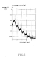
- FIG. 5 is a graph illustrating the spectrum of amplitude information Amp(t), which is expressed using 16-time sampling, with the transverse axis representing frequency [MHz] and the longitudinal axis representing magnitude [dB].
- phase information ⁇ 2(t) calculated by the phase detector 22 is input to an adder 24 and thus is phase-converted on the basis of phase data PD for frequency conversion according to the desired conversion frequency f1.
- the frequency conversion by the desired conversion frequency f1 is executed with respect to modulated signals MOD_I2(t) and MOD_Q2(t) of a sampling frequency 'Fs2' in such a manner that phase conversion is endowed (addition/subtraction) to the phase information ⁇ 2(t).
- the phase data (PD) for frequency conversion includes a phase change width obtained by quantifying the phase change of a signal according to the desired conversion frequency f1 for every single sampling data of the signal output from the digital frequency converter 2. That is, the phase data PD for frequency conversion is obtained by sampling each frequency '2 ⁇ f1' according to the desired conversion frequency f1 with a sampling frequency 'Fs3p' of the signal output from the digital frequency converter 2.
- the phase data (PD) for frequency conversion is expressed as a number being a power of 2.
- a signal frequency-converted by the desired conversion frequency f1 should have a high sampling frequency corresponding to the conversion frequency f1.
- a signal frequency-converted by the desired conversion frequency f2 may have a lower frequency than that of the signal frequency-converted by the conversion frequency f1. Executing the frequency conversion in two steps lowers the sampling frequency, thereby reducing circuit size and power consumption.
- the phase change for frequency conversion by the conversion frequency f2 is endowed.
- the sampling frequency Fs2 of a signal output from the adder 24 is '1/MP1' times as large as the sampling frequency Fs3p of a signal outputted from the digital frequency converter 2.
- phase data (PD) for frequency conversion of 'P' bits (P is a positive integer) according to the desired conversion frequency f1 are calculated on the basis of the sampling frequency Fs3p of a signal outputted from the digital frequency converter 2, a value obtained by multiplying phase data of lower 'Q' figures [bit] (Q is a positive integer) from among the phase data PD for frequency conversion by 'MP1' is determined to be a phase change width every one sampling for a signal outputted from the phase detector 22.
- phase data of lower 'Q' figures [bit] are separated from the phase data PD for frequency conversion in a data separation unit 25, and the phase data of lower 'Q' figures [bit] are multiplied by 'MP1' in a data amplification unit 26. Then, the phase data multiplied by 'MP1' is accumulated and added in an accumulator 27, which contains a register 27A and an adder 27B operating at a sampling frequency Fs2, so that it is possible to calculate phase change for frequency conversion by which a frequency can be set in the frequency step of conversion frequency 'fl/2 p ' (i.e., conversion of frequency f2 corresponding to lower 'Q' figures [bit] from among the phase data PD for frequency conversion).
- phase change calculated in the conversion of frequency f2 is added to the phase information ⁇ 2(t) output from the phase detector 22 for each sample data to generate phase information ⁇ 3(t).
- the phase information of a signal generated can be obtained as the phase information ⁇ 3(t) output from the adder 24 when the frequency of the modulated signals MOD_I2(t) and MOD_Q2(t) increases by the conversion frequency f2.
- the phase information of a signal to be generated in the case of decreasing the frequency of the modulated signals MOD_I2(t) and MOD_Q2(t) can be obtained by replacing the adder 24 with a subtractor and by subtracting phase change data output from the accumulator 27 from the phase information ⁇ 2(t) calculated in the phase detector 22.
- the resulting upsampled signal is then input to an adder 29.
- the adder 29 converts f3 as a function of the information received from the interpolator 28. That is, the phase data of upper 'P-Q' figures [bit] from among the phase data (PD) for frequency conversion of 'P' figures [bit] according to the desired conversion frequency f1 are determined to be a phase change of a width corresponds to each sampling for a signal outputted from the interpolator 28. The phase data of upper 'P-Q' figures [bit] are separated from the phase data PD for frequency conversion in the data separation unit 25.
- phase data separated by the data separation unit 25 is accumulated and added in an accumulator 30 which contains a register 30A and an adder 30B operating on a sampling frequency Fs3p.
- accumulator 30 which contains a register 30A and an adder 30B operating on a sampling frequency Fs3p.
- the phase change calculated in corresponding frequency f3 is added to the phase information ⁇ 4(t) output from the interpolator 28 for each sampling, thereby generating phase information ⁇ 5(t).
- the adding operation of the adder 29 is performed to add the phase change of 'P-Q' figures [bit] outputted by the accumulator 30 to a signal of upper 'P-Q' figures [bit] from among the phase information ⁇ 4(t) outputted from the interpolator 28.
- the phase information of a generated signal can be obtained by replacing the adder 24 with a subtractor and subtracting phase change data output by the accumulator 30 from the phase information ⁇ 4(t) calculated in the interpolator 28 when the frequency of the modulated signals MOD_I2(t) and MOD_Q2(t) decreases.
- FIG. 6 is a graph illustrating the spectrum of phase information ⁇ 3(t) obtained after the phase information ⁇ 1(t) shown in FIG. 4 undergoes frequency conversion for a normalized frequency of 0.402662489 with a sampling frequency of one.
- the transverse axis represents phase [ ⁇ ] and the longitudinal axis represents magnitude [dB].
- the spectrum shown in FIG. 6 shows a high peak around phase zero.
- a high peak shown in the spectrum increases the length of operation language required to perform sampling frequency conversion of the phase information ⁇ 3(t) in the interpolator 28, thereby increasing power consumption in the interpolator 28.
- the filter for limiting a signal of an unnecessary frequency band after upsampling should be capable of achieving a considerable amount attenuation of stop band.
- the filter should be a high-order filter which consumes increased power.
- the conversion frequency f2 it is necessary to limit the value of the conversion frequency f2 within a range where there is no increase of the spectrum peak caused by the phase processing for conversion of the frequency f2 by the adder 24 and the accumulator 27.
- the range of the conversion frequency f2 should also avoid large difference changes of operation language length and the filter order in the interpolator 28 between the time when phase is processed and when phase is not processed.
- a roll-off filter is installed at the following end of the interpolator 28 to perform waveform shaping for an input modulated signal and then phase information and amplitude information are detected in the phase detector 22 and the amplitude detector 23, respectively.
- FIG. 7 is a graph illustrating the spectrum of phase information of a QPSK signal expressed using 16-time sampling, with the transverse axis representing phase [ ⁇ ] and the longitudinal axis representing magnitude [dB].
- FIG. 8 is a graph illustrating the spectrum of amplitude information of a QPSK signal), which is expressed using 16-time sampling, with the transverse axis representing frequency [MHz] and the longitudinal axis representing magnitude [dB].
- phase conversion corresponding to frequency conversion by desired conversion frequency f1 may be achieved by only one of the two-side phase conversion.
- a sampling frequency of an inputmodulated signal is upsampled by the interpolator 21 and converted into phase information and amplitude information of a polar coordinate type by the phase detector 22 and the amplitude detector 23.
- the amplitude information becomes amplitude information output from the digital frequency converter.
- phase change output from the accumulator 27 is added to the phase information output from the phase detector 22 using the adder 24.
- phase change for frequency conversion by which a frequency can be set in the frequency step of conversion frequency 'fl/2 P' (i.e., frequency conversion of the conversion frequency f2 corresponding to lower 'Q' figures [bit] from among the phase data PD for frequency conversion), is added to phase information output from the phase detector 22.
- phase change for frequency conversion by which a frequency can be set in the frequency step of conversion frequency 'f1 /2 P-Q, (i.e., frequency conversion of the conversion frequency f3 corresponding to upper 'P-Q' figures [bit] from among the phase data PD for frequency conversion), is added to phase information outputfrom the interpolator 28.
- Phase information output from the adder 29 is converted into discontinuous phase information represented in angles of 0 to 2 ⁇ by means of the wrap circuit 31, and is input to the COS_ROM 32 and SIN_ROM 33 to generate phase-modulated signals Phase_I(t) and Phase_Q(t) of the orthogonal coordinate type.
- the phase-modulated signals Phase_I(t) and Phase_Q(t) become phase information output from the digital frequency converter.
- the phase information can be output as phase-modulated signals Phase_I(t) and Phase_Q(t) of the orthogonal coordinate type from the digital frequency converter.
- the phase information of a signal to be generated in the case of decreasing the frequency of an inputted modulated signal can be obtained by replacing the adders 24 and 29 with subtractors and by subtracting the phase change resulting from frequency conversion of conversion frequency f2 from the phase information or phase change resulting from frequency conversion of conversion frequency f3 from the phase information.
- a digital frequency converter can easily achieve frequency conversion for the phase information of an inputted modulated signal using only simple adders/subtractors, without using a multiplier.
- frequency conversion for a phase-modulated signal of the orthogonal coordinate type in the prior art requires four multipliers, one adder and one subtractor, where the present invention can easily achieve frequency conversion using only simple adders/subtractors.
- Such a construction lacking a multiplier reduces operational complexity, circuit size and power consumption.
- frequency conversion is executed through two divided steps at the front end and the rear end of the interpolator 28 which performs 'MP1'-time upsampling for a sampling frequency, so that it is possible to lower an operational frequency of a circuit in front of the interpolator 28 according to a sampling frequency.
- a sampling frequency is determined according to the signal. The sampling frequency is obtained after frequency conversion, so that the sampling frequency of a signal increases and thus the operational frequency of the digital frequency converter also increases.
- the adder 24 and the accumulator 27 can operate with a frequency of '1/MP1'.
- phase data PD for frequency conversion of 'P' bits where P is a positive integer according to the desired conversion frequency f1 are calculated on the basis of the sampling frequency Fs3p of a signal outputted from the digital frequency converter
- phase data of lower 'Q' bits are separated from the phase data PD for frequency conversion in the data separation unit 25, and the phase data of lower 'Q' bits are multiplied by 'MP1' in the data amplification unit 26, so that it is possible to reduce the length of operation language by one bit per two times in the accumulator 27.
- a digital frequency converter According to the present invention, sampling frequency of polar coordinate phase information is converted into a phase-modulated signal of the orthogonal coordinate type. Therefore, conversion of a sampling frequency can be easily achieved through at least one-half processing, as compared to the conversion of a sampling frequency for a phase-modulated signal of the orthogonal coordinate type.
- two filters for limiting an unnecessary frequency band are required, even when processing a baseband signal, to process a real-axis signal and an imaginary-axis signal.
- four filters are required for the processing of an IF signal.
- phase information of a real-axis signal needs to be processed. This is true not only for the processing of a baseband signal but also for the processing of an IF signal. In effect, only one filter is required that limits an unnecessary frequency band when converting the sampling frequency.
- the amount of operation for a filter according to an embodiment of the present invention using the polar coordinate type is reduced by three quarters in the case of processing an IF signal and by half in the case of processing a baseband signal.
- Such a reduction in operational complexity reduces the size of circuit for the digital frequency converter, and therefore reduces power consumption.
- an output signal of the accumulator 30 is added to a signal of upper 'P-Q' bits from among an output signal of the interpolator 28 in the adder 29, so that it is possible to reduce the length of operation language of the adder 29 for a signal obtained after conversion of a sampling frequency, which inevitably increases when frequency conversion and sampling frequency conversion are executed for the phase information of an inputted modulated signal.
- the size of the circuit for the digital frequency converter is reduced, thereby reducing power consumption.
- aliasing may be prevented in the polar coordinate phase and amplitude information, even though the polar coordinate phase and amplitude information converted by the phase detector 22 and the amplitude detector 23 have a wider frequency bandwidth than that of the inputted modulated signal.
- the digital frequency converter according to the present invention can produce output with reduced degradation in conversion error, noise, etc. while simultaneously providing a reduced circuit size and reduced power consumption.
Landscapes
- Digital Transmission Methods That Use Modulated Carrier Waves (AREA)
- Amplitude Modulation (AREA)
Applications Claiming Priority (4)
| Application Number | Priority Date | Filing Date | Title |
|---|---|---|---|
| JP2003398913A JP4445248B2 (ja) | 2003-11-28 | 2003-11-28 | ディジタル周波数コンバータ |
| JP2003398913 | 2003-11-28 | ||
| KR1020040085231A KR100594076B1 (ko) | 2003-11-28 | 2004-10-25 | 디지털 주파수 컨버터 |
| KR2004085231 | 2004-10-25 |
Publications (3)
| Publication Number | Publication Date |
|---|---|
| EP1536554A2 true EP1536554A2 (fr) | 2005-06-01 |
| EP1536554A3 EP1536554A3 (fr) | 2005-07-13 |
| EP1536554B1 EP1536554B1 (fr) | 2008-08-13 |
Family
ID=34467827
Family Applications (1)
| Application Number | Title | Priority Date | Filing Date |
|---|---|---|---|
| EP04028256A Expired - Lifetime EP1536554B1 (fr) | 2003-11-28 | 2004-11-29 | Convertisseur de fréquence numérique |
Country Status (3)
| Country | Link |
|---|---|
| US (1) | US7515647B2 (fr) |
| EP (1) | EP1536554B1 (fr) |
| CN (1) | CN100448163C (fr) |
Cited By (2)
| Publication number | Priority date | Publication date | Assignee | Title |
|---|---|---|---|---|
| WO2008001269A3 (fr) * | 2006-06-28 | 2008-05-15 | Nxp Bv | Conversion phase-fréquence améliorée pour émetteurs polaires |
| WO2007144806A3 (fr) * | 2006-06-12 | 2008-10-16 | Nxp Bv | Générateur de signal polaire |
Families Citing this family (3)
| Publication number | Priority date | Publication date | Assignee | Title |
|---|---|---|---|---|
| KR100841433B1 (ko) * | 2006-06-19 | 2008-06-25 | 삼성전자주식회사 | Dat가 장착된 bpsk 변조방식을 적용한 폴라 송신기 |
| US7545232B2 (en) * | 2007-06-22 | 2009-06-09 | Infineon Technologies Ag | Polar modulator arrangement and polar modulation method |
| CN103178783B (zh) * | 2011-12-21 | 2017-02-08 | 北京普源精电科技有限公司 | 求和调制信号发生器 |
Family Cites Families (12)
| Publication number | Priority date | Publication date | Assignee | Title |
|---|---|---|---|---|
| US4176319A (en) * | 1975-12-04 | 1979-11-27 | Kahn Leonard R | Double sideband transmission system |
| US4972440A (en) * | 1988-09-23 | 1990-11-20 | Hughes Aircraft Company | Transmitter circuit for efficiently transmitting communication traffic via phase modulated carrier signals |
| US5930301A (en) * | 1996-06-25 | 1999-07-27 | Harris Corporation | Up-conversion mechanism employing side lobe-selective pre-distortion filter and frequency replica-selecting bandpass filter respectively installed upstream and downstream of digital-to-analog converter |
| US5705959A (en) * | 1996-10-08 | 1998-01-06 | The United States Of America As Represented By The Secretary Of The Air Force | High efficiency low distortion amplification |
| US6043707A (en) * | 1999-01-07 | 2000-03-28 | Motorola, Inc. | Method and apparatus for operating a radio-frequency power amplifier as a variable-class linear amplifier |
| JP3323824B2 (ja) * | 1999-02-22 | 2002-09-09 | 松下電器産業株式会社 | クロック生成回路 |
| FR2791506B1 (fr) | 1999-03-23 | 2001-06-22 | France Telecom | Emetteur radiofrequence a fort degre d'integration et avec annulation d'image, eventuellement auto-calibree |
| FR2810473B1 (fr) | 2000-06-15 | 2002-10-25 | Sagem | Dispositif de production d'un signal radioelectrique module en phase et en amplitude et procede de production d'un tel signal |
| JP4429533B2 (ja) * | 2001-01-29 | 2010-03-10 | 三星電子株式会社 | 周波数変換器 |
| US7047264B2 (en) * | 2001-03-02 | 2006-05-16 | Samsung Electronics Co., Ltd. | Frequency converter |
| US6621366B1 (en) * | 2001-12-07 | 2003-09-16 | Analog Devices, Inc. | Parallel-process digital modulator structures and methods |
| KR100539929B1 (ko) * | 2001-12-15 | 2005-12-28 | 삼성전자주식회사 | 디지털 주파수 변조기 |
-
2004
- 2004-11-24 US US10/996,729 patent/US7515647B2/en not_active Expired - Fee Related
- 2004-11-29 CN CNB2004100973939A patent/CN100448163C/zh not_active Expired - Fee Related
- 2004-11-29 EP EP04028256A patent/EP1536554B1/fr not_active Expired - Lifetime
Cited By (4)
| Publication number | Priority date | Publication date | Assignee | Title |
|---|---|---|---|---|
| WO2007144806A3 (fr) * | 2006-06-12 | 2008-10-16 | Nxp Bv | Générateur de signal polaire |
| US8872596B2 (en) | 2006-06-12 | 2014-10-28 | Nxp, B.V. | Polar signal generator |
| WO2008001269A3 (fr) * | 2006-06-28 | 2008-05-15 | Nxp Bv | Conversion phase-fréquence améliorée pour émetteurs polaires |
| US8086189B2 (en) | 2006-06-28 | 2011-12-27 | Nxp B.V. | Phase-to-frequency conversion for polar transmitters |
Also Published As
| Publication number | Publication date |
|---|---|
| CN1622449A (zh) | 2005-06-01 |
| US7515647B2 (en) | 2009-04-07 |
| EP1536554B1 (fr) | 2008-08-13 |
| EP1536554A3 (fr) | 2005-07-13 |
| CN100448163C (zh) | 2008-12-31 |
| US20050117662A1 (en) | 2005-06-02 |
Similar Documents
| Publication | Publication Date | Title |
|---|---|---|
| CA2033301C (fr) | Dispositif de modulation modifiant le signal d'entree pour corriger les non-linearites d'amplification | |
| US6647073B2 (en) | Linearisation and modulation device | |
| US8626082B2 (en) | Polar feedback receiver for modulator | |
| US6097259A (en) | Modulator and modulation method for orthogonally modulating digital baseband signals | |
| JP3699602B2 (ja) | プリディストーション装置及びその方法 | |
| JP3317964B1 (ja) | 位相検出回路および受信機 | |
| US20040203542A1 (en) | Pre-distortion apparatus and method for recovering nonlinear distortion of high power amplifier | |
| JP4633902B2 (ja) | デジタルダウンコンバータ | |
| JP2010507965A (ja) | 無線周波数増幅器のスイッチ変調 | |
| US5629961A (en) | Transmitter apparatus for mobile satellite communication terminal having an envelope equalizer | |
| JP2009218770A (ja) | 歪み補償係数更新装置および歪み補償増幅器 | |
| EP1536554B1 (fr) | Convertisseur de fréquence numérique | |
| US20110051843A1 (en) | Transmission circuit | |
| US8655292B2 (en) | Amplifier circuit, transmitter, and method of controlling amplifier circuit | |
| KR100594076B1 (ko) | 디지털 주파수 컨버터 | |
| JP2008167289A (ja) | 送信装置 | |
| US7280610B2 (en) | Data converter, signal generator, transmitter and communication apparatus using the data converter or the signal generator, and data conversion method | |
| KR100251781B1 (ko) | 디지탈통신시스템의전력증폭기선형화장치및방법 | |
| KR100251385B1 (ko) | 전력증폭기의 선형화장치 및 방법 | |
| JP3842396B2 (ja) | デジタル変調装置 | |
| JP2001103104A (ja) | ディジタル無線装置 | |
| CN119448949A (zh) | 数字预失真电路以及用来在数字预失真电路中减少限幅噪声的方法 | |
| CN118508984A (zh) | 相位补偿电路、方法、发射机、接收机、终端设备和芯片 | |
| US20120243582A1 (en) | Transmitter and communication device | |
| JP3893197B2 (ja) | デジタル変調回路 |
Legal Events
| Date | Code | Title | Description |
|---|---|---|---|
| PUAI | Public reference made under article 153(3) epc to a published international application that has entered the european phase |
Free format text: ORIGINAL CODE: 0009012 |
|
| PUAL | Search report despatched |
Free format text: ORIGINAL CODE: 0009013 |
|
| 17P | Request for examination filed |
Effective date: 20041129 |
|
| AK | Designated contracting states |
Kind code of ref document: A2 Designated state(s): AT BE BG CH CY CZ DE DK EE ES FI FR GB GR HU IE IS IT LI LU MC NL PL PT RO SE SI SK TR |
|
| AX | Request for extension of the european patent |
Extension state: AL HR LT LV MK YU |
|
| AK | Designated contracting states |
Kind code of ref document: A3 Designated state(s): AT BE BG CH CY CZ DE DK EE ES FI FR GB GR HU IE IS IT LI LU MC NL PL PT RO SE SI SK TR |
|
| AX | Request for extension of the european patent |
Extension state: AL HR LT LV MK YU |
|
| AKX | Designation fees paid |
Designated state(s): DE FR GB |
|
| GRAP | Despatch of communication of intention to grant a patent |
Free format text: ORIGINAL CODE: EPIDOSNIGR1 |
|
| GRAS | Grant fee paid |
Free format text: ORIGINAL CODE: EPIDOSNIGR3 |
|
| GRAA | (expected) grant |
Free format text: ORIGINAL CODE: 0009210 |
|
| AK | Designated contracting states |
Kind code of ref document: B1 Designated state(s): DE FR GB |
|
| REG | Reference to a national code |
Ref country code: GB Ref legal event code: FG4D |
|
| REF | Corresponds to: |
Ref document number: 602004015708 Country of ref document: DE Date of ref document: 20080925 Kind code of ref document: P |
|
| PLBE | No opposition filed within time limit |
Free format text: ORIGINAL CODE: 0009261 |
|
| STAA | Information on the status of an ep patent application or granted ep patent |
Free format text: STATUS: NO OPPOSITION FILED WITHIN TIME LIMIT |
|
| 26N | No opposition filed |
Effective date: 20090514 |
|
| PGFP | Annual fee paid to national office [announced via postgrant information from national office to epo] |
Ref country code: FR Payment date: 20131115 Year of fee payment: 10 Ref country code: DE Payment date: 20131113 Year of fee payment: 10 Ref country code: GB Payment date: 20131112 Year of fee payment: 10 |
|
| REG | Reference to a national code |
Ref country code: DE Ref legal event code: R119 Ref document number: 602004015708 Country of ref document: DE |
|
| GBPC | Gb: european patent ceased through non-payment of renewal fee |
Effective date: 20141129 |
|
| REG | Reference to a national code |
Ref country code: FR Ref legal event code: ST Effective date: 20150731 |
|
| PG25 | Lapsed in a contracting state [announced via postgrant information from national office to epo] |
Ref country code: GB Free format text: LAPSE BECAUSE OF NON-PAYMENT OF DUE FEES Effective date: 20141129 Ref country code: DE Free format text: LAPSE BECAUSE OF NON-PAYMENT OF DUE FEES Effective date: 20150602 |
|
| PG25 | Lapsed in a contracting state [announced via postgrant information from national office to epo] |
Ref country code: FR Free format text: LAPSE BECAUSE OF NON-PAYMENT OF DUE FEES Effective date: 20141201 |