EP1536596B1 - Module de gestion et procédé pour configurer un module de gestion - Google Patents
Module de gestion et procédé pour configurer un module de gestion Download PDFInfo
- Publication number
- EP1536596B1 EP1536596B1 EP03027510A EP03027510A EP1536596B1 EP 1536596 B1 EP1536596 B1 EP 1536596B1 EP 03027510 A EP03027510 A EP 03027510A EP 03027510 A EP03027510 A EP 03027510A EP 1536596 B1 EP1536596 B1 EP 1536596B1
- Authority
- EP
- European Patent Office
- Prior art keywords
- driver module
- signal
- electrical devices
- signals
- accordance
- Prior art date
- Legal status (The legal status is an assumption and is not a legal conclusion. Google has not performed a legal analysis and makes no representation as to the accuracy of the status listed.)
- Expired - Lifetime
Links
- 238000000034 method Methods 0.000 title claims abstract description 26
- 230000004044 response Effects 0.000 claims abstract description 92
- 238000012360 testing method Methods 0.000 claims abstract description 44
- 230000006870 function Effects 0.000 claims description 21
- 238000005259 measurement Methods 0.000 claims description 7
- 230000036962 time dependent Effects 0.000 claims 7
- 230000005540 biological transmission Effects 0.000 claims 2
- 230000008054 signal transmission Effects 0.000 claims 1
- 230000001419 dependent effect Effects 0.000 abstract description 2
- 238000011156 evaluation Methods 0.000 description 10
- 238000001514 detection method Methods 0.000 description 9
- 238000004519 manufacturing process Methods 0.000 description 6
- 230000001939 inductive effect Effects 0.000 description 5
- 239000003990 capacitor Substances 0.000 description 3
- 238000011161 development Methods 0.000 description 2
- 230000018109 developmental process Effects 0.000 description 2
- 238000009434 installation Methods 0.000 description 2
- 230000008569 process Effects 0.000 description 2
- 230000008439 repair process Effects 0.000 description 2
- 238000003860 storage Methods 0.000 description 2
- 230000015572 biosynthetic process Effects 0.000 description 1
- 230000008859 change Effects 0.000 description 1
- 238000006243 chemical reaction Methods 0.000 description 1
- 238000004891 communication Methods 0.000 description 1
- 238000010276 construction Methods 0.000 description 1
- 230000002950 deficient Effects 0.000 description 1
- 230000004069 differentiation Effects 0.000 description 1
- 238000009826 distribution Methods 0.000 description 1
- 239000000463 material Substances 0.000 description 1
- 238000012545 processing Methods 0.000 description 1
- 230000002123 temporal effect Effects 0.000 description 1
- 230000001052 transient effect Effects 0.000 description 1
Images


Classifications
-
- H—ELECTRICITY
- H04—ELECTRIC COMMUNICATION TECHNIQUE
- H04L—TRANSMISSION OF DIGITAL INFORMATION, e.g. TELEGRAPHIC COMMUNICATION
- H04L12/00—Data switching networks
- H04L12/28—Data switching networks characterised by path configuration, e.g. LAN [Local Area Networks] or WAN [Wide Area Networks]
- H04L12/40—Bus networks
- H04L12/40006—Architecture of a communication node
- H04L12/40032—Details regarding a bus interface enhancer
-
- H—ELECTRICITY
- H04—ELECTRIC COMMUNICATION TECHNIQUE
- H04L—TRANSMISSION OF DIGITAL INFORMATION, e.g. TELEGRAPHIC COMMUNICATION
- H04L12/00—Data switching networks
- H04L12/28—Data switching networks characterised by path configuration, e.g. LAN [Local Area Networks] or WAN [Wide Area Networks]
- H04L12/40—Bus networks
- H04L2012/40267—Bus for use in transportation systems
- H04L2012/40273—Bus for use in transportation systems the transportation system being a vehicle
-
- H—ELECTRICITY
- H04—ELECTRIC COMMUNICATION TECHNIQUE
- H04L—TRANSMISSION OF DIGITAL INFORMATION, e.g. TELEGRAPHIC COMMUNICATION
- H04L43/00—Arrangements for monitoring or testing data switching networks
- H04L43/50—Testing arrangements
Definitions
- the present invention relates to a driver module for a motor vehicle electrical system and a method for configuring such a driver module.
- driver modules can serve with at least one driver which has an electrical or electronic load switch which opens or closes a load circuit containing the respective load or the respective load in response to a corresponding switching signal and thus the consumer or the load on or off. off.
- sensors or consumers also deliver signals that are to be supplied to corresponding devices.
- drivers are therefore also understood as devices which alternatively or additionally serve to transmit signals or data from electrical devices of the motor vehicle electrical system to other devices, for example a central control. These may be, for example, consumer diagnostic devices or even sensors.
- a special driver is provided in each case for a given electrical device of a motor vehicle electrical system in order to control it or to process its signals.
- Encodings are used to assign different lines of a wiring harness to an electrical device and a particular driver. For example, color-coded lines can be used. If a driver module with multiple drivers is used, in order to avoid reverse polarity, and thus a permutation of electrical equipment specific drivers, connectors with a coding in the form of guides or mechanical locking elements are used, the production of a connector in only one correct relative position make sure the contact elements of each connector to a harness to those of the driver module.
- the driver module includes a processor that controls the connected electrical devices.
- a method for the configuration of a motor vehicle electrical system with a control device for at least two connected electrical devices is known, are applied to the predetermined electrical test signals, response signals are detected, which reflect the responses of the electrical devices to the respective test signals, to determine predetermined types of connected electrical Devices are compared from the response signals data with corresponding predetermined reference data for possible given types of electrical equipment are compared, and are set in accordance with the comparison results of the determined types corresponding parameters for the connected electrical equipment.
- the US-6,356,826-B discloses an intelligent power distribution system for vehicles and a method of manufacturing the system.
- the power is distributed to the loads via intelligent connection terminals, the terminals being mounted at desired locations on a cable whose message communication bus is used to communicate control commands to electronic controllers which control the operation of the terminal.
- the present invention has for its object to enable the installation of a vehicle electrical system and in particular the connection of electrical equipment to these in a simple, but reliable manner.
- the object is achieved by a method for configuring a configurable driver module having the features of claim 1.
- a configurable driver module which comprises at least two drivers for electrical devices connected to inputs and / or outputs of the driver module, with respect to at least two electrical devices connected to the driver module via the inputs and / or outputs applied to the inputs and outputs predetermined electrical test signals detected response signals representing the responses of the electrical devices to the respective test signals, for determining predetermined types of connected electrical equipment from the response signals determined data with corresponding predetermined reference data for possible predetermined types of electrical devices, for which the driver module is provided, compared, and depending on the comparison results of the determined types corresponding parameters for the driver module and / or connected to the inputs and outputs a driver and / or the electrical equipment connected to it.
- the object is further achieved by a configurable driver module having the features of claim 13.
- the configurable driver module comprises at least two drivers for electrical devices, wherein the drivers are respectively connected to inputs and / or outputs of the driver module, a memory device in which reference data for identifying predetermined types of electrical devices are stored, a configuration device by means of which at least one test signal output device or the driver for the delivery of test signals to the input and / or Outputs are controlled, and at least one detecting means for detecting response signals representing the responses of the electrical devices to the respective test signals, wherein the configuration means is further adapted to detected values or the timings of the response signals with corresponding predetermined reference data for possible types of to compare the driver module connectable electrical equipment, and depending on the comparison results of the identified types corresponding parameters for the driver module and / or connected to the inputs and outputs drivers and / or the electrical equipment connected thereto.
- a driver module used with drivers is used in a motor vehicle electrical system.
- drivers are generally understood to mean any devices that can be used to operate electrical devices or devices, in particular those of a motor vehicle electrical system.
- the electrical devices may be, for example, sensors or loads or loads, such as electric motors or lamps.
- the drivers can be designed in particular for switching on and off of the loads or loads supplied to them switching signals out.
- the driver module is configurable. This means that it can be adapted to its use, for example, by setting parameters. In particular, it may, for example, be adaptable in terms of its properties to the electrical devices connected thereto, so that they are adapted according to their specifications by the drivers of the driver module can be controlled.
- the configuration can only refer to the driver module, whereby the drivers themselves are not configurable, but only their connections to inputs and outputs or signal channels. Preferably, however, the drivers provided in the driver module are themselves configurable.
- the configuration parameters may be, for example, maximum current or voltage values for load switches of the respective driver, which are given by the electrical device connected to these, or also the assignment of the driver to inputs or outputs.
- driver module is intended for use with electrical devices that can be divided into predetermined types that are recognized during configuration.
- the driver module In order to carry out an automatic configuration of the driver module as a function of the electrical devices connected thereto, it is initially provided that predetermined electrical test signals are applied to the inputs or outputs to which the electrical devices are connected. Since the normal inputs or outputs are used, therefore, according to the invention no additional connections between the electrical devices and the driver module are necessary to allow automatic configuration.
- the driver module according to the invention has the configuration device by means of which at least one test signal output device or the drivers for outputting test signals to the inputs or outputs can be controlled.
- the test signals can be delivered in parallel or else in a predetermined time sequence.
- Response signals are then detected which reflect the responses of the connected electrical devices to the respective test signals.
- Responses are understood to be, in particular, current values or courses or voltage values or courses at the inputs or outputs.
- the response signals can basically be given by these current or voltage values or characteristics. However, it is also possible to use other signals that only indirectly reflect these values or gradients.
- only extreme values of the responses or response signals for example peak values, can be used.
- only one value of a response and / or a response signal can be used; however, several values can also be processed.
- the driver module has the at least one detection device for detecting response signals.
- electrical devices are classified into types that are distinguishable from one another by the responses to the test signals.
- the temporal courses of current signals differ as answers for essentially resistive consumers from those for consumers having inductances, as is the case, for example, with electric motors.
- distinctions can be made about the values of, for example, the currents at predetermined voltages supplied to the electrical devices, so that, for example, ohmic consumers can be distinguished according to their resistance.
- the driver module In order to determine such predetermined types of the electrical devices connected to the driver module, data is determined from the response signals, which are then compared with reference data that are characteristic of the types of electrical devices.
- the driver module has the memory device in which the reference data for identifying predetermined types of electrical devices and parameters for the corresponding configuration of the driver module and / or the driver and / or the electrical devices connected thereto are stored as a function of the respective types.
- the configuration device is designed to compare the detected values or time profiles of the response signals with corresponding predetermined reference data. For this purpose, these values and / or courses can be used directly, but reference values of parameters can be derived on the basis of the values and / or courses, which then serve for comparison.
- the reference data may be predetermined by specifications for the given types of electrical equipment or may be obtained by measurements on corresponding electrical equipment defining the types.
- the reference data may in particular be stored in a table or in the manner of a database in data records which, in addition to the reference data, contain the type and optionally the parameters or parameter values used for the configuration.
- parameters determined for the driver module and / or the drivers connected to the inputs or outputs and / or the electrical devices connected thereto are then set for the determined types.
- the configuration is carried out by the configuration device which sets the corresponding parameters and can be connected to the drivers, for example.
- the invention thus makes it possible to use driver modules with drivers independently of the electrical devices that are actually connected to them, by automatically configuring the driver module, optionally including the drivers contained in it and / or the electrical devices connected to them, in dependence on the devices connected thereto becomes.
- the parameters set after the comparison may, in a preferred embodiment, be supplied or interrogated by an external device to which the determined types have been transmitted and which has corresponding data.
- the parameters for the corresponding configuration of the driver module and / or the driver and / or the electrical devices connected thereto are stored in the memory device.
- the parameters stored in the memory device for configuring the driver module and / or the driver and / or the electrical devices connected thereto can then in particular be used in the driver module according to the invention. For this purpose, after determining the type of a connected electrical device, in particular from the memory device from the corresponding data record with respect to the type, the corresponding parameters can be read out and set.
- driver module In principle, it is possible to keep the assignment of drivers and the inputs and outputs connected to them configurable, but preferably the drivers are permanently connected to the inputs or outputs, the configuration then being able to take place solely by configuring the drivers. This simplifies the construction of the driver module according to the invention.
- driver modules are often connected via corresponding signal channels with these devices and in particular the central control unit. It is then preferred for a driver module to be used with signal channels to be allocated to the electrical devices, via the signals for controlling the drivers connected to the electrical devices or for transmitting data or measurement signals from and to the electrical devices and / or the connected thereto Drivers are transferable, and that in the configuration at least one input or output or a driver of the driver module and thus the corresponding electrical device and a signal channel are assigned to each other.
- an interface for at least two signal channels is provided by an external device, and that the configuration device is designed to assign one of the signal channels to a driver.
- the signal channels may be channels in a bus, such as a CAN bus, so that the interface is also a corresponding bus interface.
- the external device may be, for example, a central control unit.
- the assignment of drivers to channels may preferably correspond to an assignment of electrical devices to signal channels.
- the configuration of the driver module may also include an association of the connected electrical devices to control or signal channels intended for or through the latter via which control or data signals are transferable from other devices to the drivers or in the reverse direction.
- the configuration device is designed to assign a signal channel and the type of electrical device connected to the corresponding driver to one another, and that a non-volatile memory is provided in which corresponding data can be stored.
- the signal channels can also be predetermined for specific electrical devices.
- the reference data for one type of electrical device include an identifier for the signal channel to be allocated.
- a pattern of the determined types is compared with predetermined possible stored reference patterns of types in which each electrical device is assigned a predetermined signal channel designated by an identifier.
- possible reference patterns of types of electrical devices and their respectively assigned sets of identifiers for signal channels are stored in a further memory device, and in that the configuration device is designed to compare a detected pattern of the types of the connected electrical devices with the reference patterns and to assign signal channels to the connected electrical devices in accordance with the result of the comparison.
- a pattern is understood to be at least an indication of which types were determined in which number. If the drivers are permanently connected to the inputs or outputs, the order of the types with regard to the inputs and outputs is also preferably taken into account.
- a driver module according to the invention can have differently constructed drivers. However, it is preferred that at least two of the drivers are substantially the same and configurable. This is preferably the case with all drivers of a driver module.
- any response signals representing the type of electrical equipment can be used.
- a current signal and / or a voltage signal is used as the response signal, which reproduces the current to or the voltage at the respective electrical device.
- a current signal and / or a voltage signal is used at the input or output connected to the respective electrical device.
- the electrical devices need not have any additional means specially designed, for example, for delivering responses or response signals. Rather, the very normal electrical properties of the electrical equipment can be used.
- At least one of the drivers has as a load switch a current-measuring MOSFET component which outputs a current signal corresponding to the load current, and in that a voltage signal generated by the current signal on a resistance element is used as the response signal.
- at least one of the drivers as a load switch to comprise a MOSFET component with a current measurement and an associated current signal output for outputting current signals corresponding to the magnitude of the current flowing between load current terminals of the MOSFET component the current signal output branch, through which the current signal flows, a resistance element is arranged, and that the detection means is adapted to detect voltage applied to the resistance element as response signals.
- MOSFET devices with a current measurement which is often referred to as a "current-sense" function, are available as finished components, which greatly facilitates the manufacture of the driver modules according to the invention.
- a resistance element is understood as meaning any component which has an electrical resistance, in particular a DC resistance, for example resistors or even diodes.
- the voltage signal is thus to be regarded as a response signal which represents the response given by the load current of an electrical device connected to the respective driver.
- individual values of a response signal can be used for comparison with reference data.
- the value of a response signal in a steady state may be used in which the corresponding test signal has a constant value accepts.
- a time profile of at least one response signal is detected after an initial time specified by the respective test signal, and on the basis of at least the time profile of the type electrical device is determined.
- the detection device it is preferable for the detection device to be designed to detect a time profile of at least one response signal, and for the configuration device to determine a type of a respective electrical device to be based on at least the detected time profile.
- electrical characteristics of the electrical devices can be used for identification by the use of a time profile, which substantially increases the number of possible distinguishable types.
- the relative development of time that is to say in a graphical illustration, the form of a corresponding signal curve, can be used for the time course.
- absolute values of the corresponding response waveform are used for identification, so that, for example, different inductive loads can be distinguished from each other.
- the comparison of the time profile of the response signals with corresponding reference data can be done in different ways.
- the configuration device of the driver module according to the invention can preferably have corresponding comparison means for comparing the individual values of the response signal with the corresponding values stored as reference data.
- the times are chosen equidistant. It is carried out as a kind of pointwise comparison of the progressions of the response signal and a corresponding reference signal for an electrical reference device defining the respective type.
- values of response signal parameters which at least partially reproduce the time profile of the response signal are determined from the detected time profile of the response signal, and that the comparison of the response signal waveforms with reference signal profiles for the respective type defining electrical reference devices by comparing the determined Values of the response signal parameters are carried out with corresponding reference values of the parameters determined for the reference signal profiles for the reference devices.
- values may be, for example, the values of maximum or minimum values of the response or reference signals in a predetermined time interval, rates of change of the response or reference signals at one or more predetermined times, or also curvatures of the course of the response or reference signal act.
- the compensation or interpolation functions which approximately represent the course given by the values can be determined by determining parameters or coefficients for such functions. For example, polynomials could be used as balancing functions.
- the configuration device of a driver module according to the invention can therefore in particular have corresponding parameter determination devices for determining values of response signal parameters and corresponding comparison means.
- jump signals are used as test signals.
- the response signals can then reproduce in particular the step response of an electrical device which may depend on its ohmic resistance, its capacitance and its inductance.
- test signal is generated by switching on or off a corresponding electrical device.
- the configuration device is designed to control one of the drivers for generating a test signal such that it closes or opens a load circuit. In this way, the effort for the formation and delivery of test signals can be minimized, so that there is a particularly simple structure of the driver module according to the invention.
- the configuration of the driver module can take place in accordance with a corresponding configuration signal fed thereto.
- the test signals are automatically output, the comparisons are carried out and the setting of the parameters is carried out.
- the configuration device is designed to output the test signals during the first startup of the driver module, to perform the comparisons and to carry out the setting of the parameters.
- the driver modules according to the invention can supply electrical devices with currents of very different magnitude, so that from this perspective it would be necessary to use cables with the same cable cross section corresponding to the maximum current. However, this would result in unnecessarily large material consumption and unnecessary weight of the cables. In addition, the drivers would have to be designed in terms of the maximum possible current.
- At least two drivers of the driver module according to the invention are configurable for parallel operation.
- a load is then connected to a very large power and thus power consumption via two lines with two drivers operated in parallel, which then drive together.
- a broad application of the driver module can take place.
- the driver connected thereto are configured for parallel operation for at least two corresponding inputs or outputs.
- the configuration device is designed to control only one driver so that one Test signal is output via only one input or one output that the detection device is designed for the simultaneous detection of response signals for all inputs and outputs, and that the configuration device is further configured to check for which inputs and outputs response signals detectable and, if the result of the check is positive, for at least two corresponding inputs and / or outputs the drivers connected for parallel operation are to be configured.
- the same signal channel can be assigned to both drivers. In this way, two drivers to be operated in parallel can easily be assigned to an electrical device which has a particularly high power consumption.
- an identifier of the electrical device is read into the driver module via a corresponding channel from a connected electrical device, which again specifies it more precisely via the parameters determined via the response signal, so that an even finer distinction of different types is made possible ,
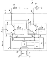
- a driver module 10 via a control and evaluation unit 12 and n identically configured, configurable driver circuits 14 1 to 14 n , via outputs 16 1 to 16 n , to the different from each other Driver module 10 to be operated electrical devices, ie here consumers or loads 18 1 to 18 n , are connected. Furthermore, it is connected via a bus interface 20 of the control and evaluation unit 12, for example, for a CAN bus, with signal channels 22 1 to 22 n of the bus 23, via the control signals for switching on and off of the loads 18 1 to 18 n the driver module 10 can be issued.
- n denotes a natural number, preferably greater than 1.
- the driver circuits 14 1 to 14 n are each formed the same, so that their structure is explained using the example of the driver circuit 14 1 .
- the driver circuit 14 1 includes as load switch an n-channel MOSFET device 24 in a so-called "high-side" arrangement, wherein its drain terminal 26 with a positive pole of a supply voltage source 28, in the example of a motor vehicle battery, and its source Terminal 30 is connected to the load 18 1 .
- the respective other terminal of the load 18 1 is grounded, with the negative terminal of the supply voltage source 28 is connected.
- the gate terminal 32 of the MOSFET component 24 is connected to a corresponding switching signal output of the control and evaluation device 20.
- the MOSFET device 24 further has a current measuring function ("current sense" function). Via a current signal output 34, a current signal is applied to a current signal branch 36 with a grounded resistor R arranged therein, the current intensity of which corresponds to the magnitude of the load current conducted through the MOSFET component 24 between the drain and source terminals 26 and 30 ,
- switching signal outputs 38 1 to 38 of the control and evaluation circuit 12 n can be as means of acting as a load switch MOSFET devices 24 of the drive circuits 14 1 to 14 n are turned off in each case connected to them loads 18 1 to 18 mono- n and become.
- the control and evaluation device 12 is powered by another voltage source 42 with voltage.
- a first memory device 44 in the form of an EEPROM
- a second memory device 46 with a nonvolatile memory a configuration device 48 and a detection device 50th
- the detection device 50 has one or more analog-to-digital converters, not shown in the figures, whose inputs are connected to the analog inputs 40 1 to 40 n in order to convert these voltage signals into digital values.
- the driver circuits 14 1 to 14 n are configurable, the signal channels 22 1 to 22 n according to the configuration switching signal outputs 38 1 to 38 n and thus driver circuits 14 1 to 14 n , outputs 16 1 to 16 n or Loads 18 1 to 18 n can be assigned.
- the switching signals and the signals at the analog inputs 40 1 to 40 n for example, it can be determined or checked how large the maximum permitted load current is or whether it has been exceeded, so that the control and evaluation device 12 then insofar as to be regarded as a configurable part of a driver with the respectively driven driver circuit.
- the control and evaluation device 12 is designed so that after the first commissioning of the driver module 10, this is automatically configured automatically in dependence on the loads 18 1 to 18 n connected thereto.
- the configuration of the driver module 10 is carried out according to the method described below according to a preferred embodiment of the invention.
- the configuration device 48 In a first connection of the driver module 10 with the supply voltage source 28 or voltage supply 42, the configuration device 48 outputs parallel or successive switching signals via the switching signal outputs 38 1 to 38 n to the driver circuits 14 1 to 14 n , in particular their gate terminals 32, by means of which the channels between the drain terminals 26 and the source terminals 30 are switched from a non-conductive to a conductive state.
- the switching signals are selected so that the voltages applied to the loads 18 1 to 18 n jump in the form of a jump function from zero to a predetermined voltage value.
- current signals are output via the corresponding current signal branches with currents corresponding to the load currents which lead to corresponding voltage signal waveforms Us1 to Usn at the analog inputs 40 1 to 40 n, which correspond to the current signal profiles and thus to the load current characteristics, and thus Represent response signals in the context of the invention.
- response signals are detected under analog-to-digital conversion in the detection device 50 and buffered.
- voltage values in equal time intervals t1 starting with the time at which the voltage at the outputs 16 1 to 16 n each jumps to the value given by the supply voltage source 28, are detected and buffered.
- the detected signal curves reproduce electrical properties of the loads 18 1 to 18 n , so that different types of the loads can be determined on the basis of the responses of the response signals.
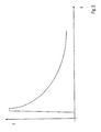
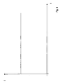
- FIGS. 2 to 4 show, by way of example, responses, ie curves of load currents I as a function of time t for various idealized electrical devices, whose properties are based on a jump in the voltage through corresponding characteristic curves for a substantially capacitive load, a constant ohmic resistance and an inductive load, such as a coil, are given.
- the response signals at the analog inputs 40 1 to 40 n would be substantially proportional to these traces.
- FIG. 2 shows the typical profile for a series connection of a resistor and a capacitor or a capacitor, wherein the characteristic curve is determined by the size of the resistor or the size of the capacitor.
- Fig. 3 shows the response of a load with purely ohmic resistance, in which virtually immediately a stationary, the size of the resistor corresponding current value is achieved without a transient process.
- Fig. 4 finally shows the response of an inductive load, such as a motor, at power-up and later power-off at time to.
- an inductive load such as a motor
- Another particular type of load is represented by light bulbs, where a very large current initially occurs because the filament has a relatively high conductivity when cold. However, the current then falls very quickly back to a lower value, since the filament heats up and thus receives a higher resistance. Thereafter, a constant current is achieved similar to an ohmic resistance. In this way, based on the course and the asymptotic value of the current not only light bulbs recognized, but also their parameters, such as the power consumption, are determined.
- references data are determined before the actual configuration, which reflect the characteristic curve or the course of the response signals of the loads, thus allowing a classification of the loads in types.
- the reference data are stored in a table in the first memory device 44 in connection with the corresponding types and the type-dependent parameters to be used for the configuration, including the identifiers of the signal channels 22 1 to 22 n .
- the signal characteristics of the corresponding reference devices themselves are not used as reference data. Rather, reference values of parameters of predefined compensation functions are determined based on constant values of analog signals for the given reference devices defining the type, which approximately reproduce the course of the analog signals for the reference devices. For example, splines can be used as compensation functions. Only the corresponding coefficients are then determined and stored as reference data for the types.
- the comparison of the response signals detected for the loads 18 1 to 18 n is now carried out in such a way that, starting from the analog signal values detected at constant time intervals, the predetermined compensation function is applied by these values whose functional form corresponds to the functional form of the compensation function used in the determination of the reference data , Values of the parameters or coefficients of the compensation function are determined so that they reproduce the detected response signals as well as possible.
- the obtained set of parameter values is compared with the corresponding reference values in the first memory device 44. With a sufficient agreement, which can be established, for example, if the amounts of the deviations of the corresponding parameters from each other each remain below a predetermined limit, a corresponding type for the load is determined. From the configuration means 48 corresponding to the type stored in the first memory means 44 parameters for the respective driver circuit 14 j are read from the first memory means and set, for example, the maximum possible current or the maximum size of a corresponding switching signal for this driver circuit and the type of Control, for example, by pulse width modulation or with a constant voltage, can affect.
- the loads 18 1 to 18 n are each assigned arbitrary predetermined signal channels 22 1 to 22 n , the assignment by specifying the outputs 16 1 to 16 n or driver circuits 14 1 to 14 n , respectively can be done to these types of connected loads and identifiers corresponding signal channels.
- These data are stored in the second memory device 46 for retrieval by a central control device.
- the data can be read out by the central control device so that it can control the respective loads by means of the driver module 10 in accordance with the types and signal channel identifications via control signals via the signal channels.
- a driver module In a second embodiment of a driver module according to the invention and a method according to the invention, only the manner of assigning signal channels is changed. For this purpose, as in the first embodiment, it is determined at which output 16 1 to 16 n which type of load is connected. This results in a pattern of types, which is given by the specification of the types determined in the order of the outputs 16 1 to 16 n .
- all possible reference patterns of types are stored in association with corresponding patterns of identifiers of signal channels.
- the configuration means compares the pattern determined with the stored patterns, and associates each load 18 j those signal channel 22 to k, which is predetermined at the same reference pattern for the type at this output 16 j.
Landscapes
- Engineering & Computer Science (AREA)
- Computer Networks & Wireless Communication (AREA)
- Signal Processing (AREA)
- Stored Programmes (AREA)
- Testing Electric Properties And Detecting Electric Faults (AREA)
- Air Bags (AREA)
- Tests Of Electronic Circuits (AREA)
Claims (22)
- Procédé pour configurer un module de gestion configurable, qui comporte au moins deux gestionnaires (141, ..., 14n) pour organes électriques (181, ..., 18n) reliés avec des entrées et/ou sorties (161, ..., 16n) du module de gestion, en ce qui concerne au moins deux organes électriques (181, ..., 18n) raccordés au module de gestion (10) par l'intermédiaire des entrées et / ou sorties (161, ..., 16n), dans lequeldes signaux électriques de test prédéfinis sont appliqués aux entrées ou sorties (161, ..., 16n),des signaux de réponse, qui restituent les réponses des organe électriques (181, ..., 18n) aux signaux de test respectifs, sont acquis,des données déterminées à partir des signaux de réponse sont comparées avec des données de référence prédéfinies correspondantes pour des types prédéfinis possibles d'organes électriques (181, ..., 18n) pour lesquels est prévu le module de gestion (10), en vue de la détermination de types prédéfinis d'organes électriques raccordés (181, ..., 18n),et des paramètres correspondant aux types déterminés pour le module de gestion (10) et/ ou les gestionnaires (141, ..., 14n) reliés avec les entrées ou sorties (161, ..., 16n) et/ou les organes électriques raccordés (181, ..., 18n) sont fixés en fonction des résultats de comparaison.
- Procédé selon la revendication 1,
caractérisé en ce
qu'un module de gestion (10) est utilisé avec des canaux de signalisation (221, ..., 22n) à affecter aux organes électriques (181, ..., 18n), par l'intermédiaire desquels des signaux destinés à l'activation des gestionnaires (141, ..., 14n) reliés avec les organes électriques (181, ..., 18n) ou destinés à la transmission de signaux de données ou de mesure peuvent être transmis depuis ou vers les organes électriques (181, ..., 18n) et/ou les gestionnaires (141, ..., 14n) reliés avec ces derniers, et
en ce que lors de la configuration, au moins une entrée ou sortie (161, ..., 16n) ou un gestionnaire (141, ..., 14n) du module de gestion (10) et ainsi l'équipement électrique correspondant (181, ..., 18n) et un canal de signalisation (221, ..., 22n) sont affectés les uns aux autres. - Procédé selon la revendication 2,
caractérisé en ce
que des canaux de signalisation (221, ..., 22n) et des types respectifs d'organes électriques (181, ..., 18n) sont affectés les uns aux autres et en ce que cette information est mise en mémoire. - Procédé selon l'une quelconque des revendications précédentes,
caractérisé en ce
qu'un signal de courant et/ou un signal de tension, qui restitue le courant ou la tension au niveau de l'organe électrique respectif (181, ..., 18n), est respectivement utilisé en tant que signal de réponse. - Procédé selon la revendication 4,
caractérisé en ce
qu'au moins un des gestionnaires (141, ..., 14n) présente un composant MOSFET (241, ..., 24n) avec mesure du courant en tant que commutateur de charge, ledit composant MOSFET délivrant un signal de courant correspondant au courant de charge et en ce qu'un signal de tension généré par le signal de courant au niveau d'un élément de résistance (R) est utilisé en tant que signal de réponse. - Procédé selon l'une quelconque des revendications précédentes,
caractérisé en ce
qu'une évolution dans le temps d'au moins un signal de réponse est acquise après un instant initial prédéfini par le signal de test respectif, et
en ce que le type d'organes électriques respectifs (181, ..., 18n) est déterminé sur la base au moins de l'évolution dans le temps. - Procédé selon la revendication 6,
caractérisé en ce
que des valeurs individuelles du signal de réponse sont acquises aux instants prédéfinis après l'instant initial, et
en ce que les valeurs individuelles acquises du signal de réponse sont comparées avec des valeurs correspondantes mémorisées en tant que données de référence pour un type donné d'organes électriques (181, ..., 18n). - Procédé selon la revendication 6 ou 7,
caractérisé en ce
que des valeurs de paramètres de signal de réponse, qui restituent au moins en partie l'évolution dans le temps du signal de réponse, sont déterminées à partir de l'évolution dans le temps acquise du signal de réponse et en ce que la comparaison des évolutions du signal de réponse avec des évolutions de signal de référence pour les organes électriques de référence définissant des types respectifs est effectuée via comparaison des valeurs déterminées des paramètres de signal de réponse avec des valeurs de référence correspondantes des paramètres déterminées pour les évolutions de signal de référence pour les organes de référence. - Procédé selon l'une quelconque des revendications précédentes,
caractérisé en ce
que des sauts de signaux sont utilisés en tant que signaux de test. - Procédé selon la revendication 9,
caractérisé en ce
que le signal de test est généré via mise sous tension ou hors tension d'un organe électrique correspondant (181, ..., 18n). - Procédé selon l'une quelconque des revendications précédentes,
caractérisé en ce
que lors de la première mise en service du module de gestion (10), les signaux de test sont automatiquement délivrés, les comparaisons sont exécutées et la fixation des paramètres est effectuée. - Procédé selon l'une quelconque des revendications précédentes,
caractérisé en ce
qu'un signal de test est délivré par un seul gestionnaire par l'intermédiaire d'une seule entrée ou une seule sortie,
en ce que pour toutes les autres entrées ou sorties, il est vérifié si des signaux de réponse appelés par le signal de test peuvent être acquis pour ces dernières, et
en ce qu'en cas de résultat positif du test pour au moins deux entrées ou sorties correspondantes, les gestionnaires ainsi reliés sont configurés pour fonctionner en parallèle via affectation du même canal de signalisation. - Module de gestion configurable avec
au moins deux gestionnaires (141, ..., 14n) pour des organes électriques (181, ..., 18n), les gestionnaires (141, ..., 14n) étant respectivement reliés avec des entrées et/ou sorties (161,..., 16n) du module de gestion (10),
avec un dispositif de stockage (44), dans lequel sont mémorisées des données de référence en vue de l'identification de types prédéfinis d'organes électriques (181, ..., 18n),
avec un dispositif de configuration (48), au moyen duquel au moins un dispositif de délivrance de signal de test ou les gestionnaires (141, ..., 14n) peuvent être activés en vue de la délivrance de signaux de test au niveau des entrées et/ou sorties (161, ..., 16n) et
avec au moins un dispositif d'acquisition (50) destiné à l'acquisition de signaux de réponse qui restituent les réponses d'organes électriques (181, ..., 18n) qui sont raccordés par l'intermédiaire des entrées et/ou sorties du module de gestion, aux signaux de test respectifs,
le dispositif de configuration (58) étant de plus conçu en vue de comparer des valeurs acquises et/ou les évolutions dans le temps des signaux de réponse avec des données de référence correspondantes prédéfinies pour des types possibles d'organes électriques (181, ..., 18n) raccordables au module de gestion (10), et en vue de déterminer les types des organes électriques raccordés en fonction des résultats de comparaison et de fixer des paramètres correspondant aux types déterminés pour le module de gestion (10) et/ou les gestionnaires (141, ..., 14n) reliés avec les entrées ou sorties (161, ..., 16n) et/ou les organes électriques raccordés (181, ..., 18n). - Module de gestion selon la revendication 13,
caractérisé en ce
que des paramètres sont mémorisés dans le dispositif de stockage (44) en vue de la configuration correspondante du module de gestion (10) et/ou des gestionnaires (141, ..., 14n) et/ou des organes électriques raccordés. - Module de gestion selon la revendication 13 ou 14,
caractérisé en ce
qu'une interface (20) est prévue pour au moins deux canaux de signalisation (221, ..., 22n) d'un dispositif externe et en ce que le dispositif de configuration (48) est conçu en vue d'assigner un des canaux de signalisation (221, ..., 22n) à un gestionnaire (141, ..., 14n). - Module de gestion selon l'une quelconque des revendications 13 à 15,
caractérisé en ce
que le dispositif de configuration (48) est conçu en vue d'affecter un canal de signalisation (221, ..., 22n) et le type de l'organe électrique (181, ..., 18n) raccordé au gestionnaire correspondant (141, ..., 14n) l'un à l'autre, et
en ce qu'une mémoire non volatile (46) est prévue, dans laquelle des données sont mémorisables en conséquence. - Module de gestion selon l'une quelconque des revendications 13 à 16,
caractérisé en ce
qu'au moins deux des gestionnaires (141, ..., 14n) sont conçus et configurables de manière identique. - Module de gestion selon l'une quelconque des revendications 13 à 17,
caractérisé en ce
qu'au moins un des gestionnaires (141, ..., 14n) comporte un composant MOSFET (241, ..., 24n) avec une mesure du courant en tant que commutateur de charge et une sortie du signal de courant (34) reliée avec, en vue de la délivrance de la grandeur du courant des signaux de courant correspondants circulant entre les connexions de courant de charge (26, 30) du composant MOSFET (221, ..., 22n), en ce qu'un élément de résistance (R) est disposé dans une branche du signal de courant (36) reliée avec la sortie du signal de courant (34), par laquelle passe le signal de courant, et
en ce que le dispositif d'acquisition (50) est conçu en vue d'acquérir des tensions appliquées au niveau de l'élément de résistance (R) en tant que signaux de réponse. - Module de gestion selon l'une quelconque des revendications 13 à 18,
caractérisé en ce
que le dispositif d'acquisition (50) est conçu en vue de l'acquisition d'une évolution dans le temps d'au moins un signal de réponse et en ce que le dispositif de configuration (48) est conçu en vue de la détermination d'un type d'un organe électrique respectif (181, ..., 18n) sur la base au moins de l'évolution dans le temps acquise. - Module de gestion selon l'une quelconque des revendications 13 à 19,
caractérisé en ce
que le dispositif de configuration (48) est conçu en vue d'activer un des gestionnaires (221, ..., 22n) en vue de la génération d'un signal de test, de telle manière que ledit gestionnaire ouvre ou ferme un circuit de courant de charge. - Module de gestion selon l'une quelconque des revendications 13 à 20,
caractérisé en ce
que le dispositif de configuration (48) est conçu en vue de délivrer les signaux de test lors de la première mise en service du module de gestion (10), de procéder aux comparaisons et d'effectuer la fixation des paramètres. - Module de gestion selon l'une quelconque des revendications 13 à 21,
caractérisé en ce
que le dispositif de configuration est conçu en vue d'activer un seul gestionnaire, de telle manière qu'un signal de test est délivré par l'intermédiaire d'une seule entrée ou d'une seule sortie,
en ce que le dispositif d'acquisition est conçu en vue de l'acquisition simultanée de signaux de réponse pour toutes les entrées et sorties,
et en ce que le dispositif de configuration est de plus conçu en vue de vérifier pour quelles entrées ou sorties des signaux de réponse peuvent être acquis et, en cas de résultat positif du test pour au moins deux entrées ou sorties correspondantes, afin de configurer les gestionnaires ainsi reliés via affectation du même canal de signalisation en vue du fonctionnement en parallèle.
Priority Applications (3)
| Application Number | Priority Date | Filing Date | Title |
|---|---|---|---|
| DE50307625T DE50307625D1 (de) | 2003-11-28 | 2003-11-28 | Treibermodul und Verfahren zur Konfiguration eines Treibermoduls |
| AT03027510T ATE366493T1 (de) | 2003-11-28 | 2003-11-28 | Treibermodul und verfahren zur konfiguration eines treibermoduls |
| EP03027510A EP1536596B1 (fr) | 2003-11-28 | 2003-11-28 | Module de gestion et procédé pour configurer un module de gestion |
Applications Claiming Priority (1)
| Application Number | Priority Date | Filing Date | Title |
|---|---|---|---|
| EP03027510A EP1536596B1 (fr) | 2003-11-28 | 2003-11-28 | Module de gestion et procédé pour configurer un module de gestion |
Publications (2)
| Publication Number | Publication Date |
|---|---|
| EP1536596A1 EP1536596A1 (fr) | 2005-06-01 |
| EP1536596B1 true EP1536596B1 (fr) | 2007-07-04 |
Family
ID=34442916
Family Applications (1)
| Application Number | Title | Priority Date | Filing Date |
|---|---|---|---|
| EP03027510A Expired - Lifetime EP1536596B1 (fr) | 2003-11-28 | 2003-11-28 | Module de gestion et procédé pour configurer un module de gestion |
Country Status (3)
| Country | Link |
|---|---|
| EP (1) | EP1536596B1 (fr) |
| AT (1) | ATE366493T1 (fr) |
| DE (1) | DE50307625D1 (fr) |
Families Citing this family (3)
| Publication number | Priority date | Publication date | Assignee | Title |
|---|---|---|---|---|
| DE102005060607A1 (de) * | 2005-12-17 | 2007-06-21 | Conti Temic Microelectronic Gmbh | Vorrichtung und Verfahren zur Erfassung und Verarbeitung von Messwerten |
| CN111930595B (zh) * | 2020-07-30 | 2022-03-15 | 长沙景嘉微电子股份有限公司 | 显卡驱动校验方法、装置、终端和介质 |
| CN114337453B (zh) * | 2021-12-29 | 2023-11-21 | 深圳市汇川技术股份有限公司 | 驱动器机型自动识别方法、装置及驱动器 |
Family Cites Families (4)
| Publication number | Priority date | Publication date | Assignee | Title |
|---|---|---|---|---|
| AU1260697A (en) * | 1996-02-21 | 1997-08-28 | Consolidated Technologies International | Multiplexed electrical system having a central controller and programmable control nodes |
| WO1999025586A2 (fr) * | 1997-11-14 | 1999-05-27 | Iws International, Inc. | Systeme de distribution de courant intelligent pour vehicules et son procede de fabrication |
| US6249060B1 (en) * | 1999-06-18 | 2001-06-19 | Jonathan P. Osha | Multiplexed cabling system for a vehicle |
| DE10203341A1 (de) * | 2002-01-29 | 2003-07-31 | Bayerische Motoren Werke Ag | Elektronisches Steuergerät für ein Kraftfahrzeug oder ein Fahrzeug-Antriebsaggregat |
-
2003
- 2003-11-28 EP EP03027510A patent/EP1536596B1/fr not_active Expired - Lifetime
- 2003-11-28 DE DE50307625T patent/DE50307625D1/de not_active Expired - Fee Related
- 2003-11-28 AT AT03027510T patent/ATE366493T1/de not_active IP Right Cessation
Non-Patent Citations (1)
| Title |
|---|
| None * |
Also Published As
| Publication number | Publication date |
|---|---|
| EP1536596A1 (fr) | 2005-06-01 |
| DE50307625D1 (de) | 2007-08-16 |
| ATE366493T1 (de) | 2007-07-15 |
Similar Documents
| Publication | Publication Date | Title |
|---|---|---|
| DE69231446T2 (de) | Intelligente lampe oder intelligenter kontakt für eine lampe | |
| EP1455278B1 (fr) | Méthode pour l'identification d'un dispositif électronique | |
| EP1039357B1 (fr) | Dispositif d'ajustage des paramètres opératoires pour plusieurs circuits intégrés programmables | |
| EP0870646B1 (fr) | Clignoteur électronique | |
| DE4240447C1 (de) | Elektronische Kennung und Erkennung einer fahrzeugspezifischen Kombination optionaler elektronischer Steuergeräte | |
| EP0393233B1 (fr) | Système de transmission de signaux | |
| DE4338462B4 (de) | Kontrollsystem für elektrische Verbraucher in Kraftfahrzeugen | |
| DE102006053959B4 (de) | Kommunikationssystem | |
| EP3973745B1 (fr) | Procédé et dispositifs pour réguler la tension de sortie d'un régulateur de tension | |
| EP1536596B1 (fr) | Module de gestion et procédé pour configurer un module de gestion | |
| WO2023170198A1 (fr) | Dispositif comprenant un appareil de communication pour le transfert de données par l'intermédiaire d'un bus de transfert de données, et système de transfert de données comprenant des dispositifs de ce type | |
| EP2240677A1 (fr) | Procédé pour contrôler au moins une bougie-crayon de préchauffage d'un moteur à combustion interne et dispositif correspondant | |
| EP2943845B1 (fr) | Dispositif et procédé de commande d'une installation de chauffage et/ou de réfrigération | |
| EP1203933B1 (fr) | Dispositif capteur pour la mesure d'au moins une grandeur | |
| DE10250169B4 (de) | Eine Abtrennung einer elektrischen Last detektierendes Gerät | |
| DE102015215783A1 (de) | Verfahren und Vorrichtung zum Konfigurieren einer Steuervorrichtung in einem Kraftfahrzeug | |
| DE102021119956A1 (de) | Testen von Stromversorgungspfaden und Verbrauchern eines Fahrzeugs | |
| EP2733818A2 (fr) | Appareil de fonctionnement multifonctions destiné à l'alimentation d'un consommateur tel qu'un module LED et son procédé de fonctionnement | |
| EP1536595B1 (fr) | Procédé pour implanter un module de gestion dans l'électronique automobile | |
| EP1702808A2 (fr) | Dispositif d'alimentation de tension pour des consommateurs dans une réseau de bord d' un véhicule utilisant plusieurs générateurs | |
| DE60302434T2 (de) | Erkennung von Anhängeranwesenheit und -typ durch Stromdetektion | |
| EP0736419A2 (fr) | Dispositif pour la commande d'au moins un appareil monté dans un véhicule | |
| DE102019213835A1 (de) | Verfahren und Vorrichtung zum Erkennen eines zusätzlichen Verbrauchers in einem Energienetz | |
| EP1011190A2 (fr) | Méthode et circuit pour surveiller une charge en régime de fontionnement | |
| EP3626973B1 (fr) | Système à vide et procédé d'identification de modules électroniques dans un tel système à vide |
Legal Events
| Date | Code | Title | Description |
|---|---|---|---|
| PUAI | Public reference made under article 153(3) epc to a published international application that has entered the european phase |
Free format text: ORIGINAL CODE: 0009012 |
|
| AK | Designated contracting states |
Kind code of ref document: A1 Designated state(s): AT BE BG CH CY CZ DE DK EE ES FI FR GB GR HU IE IT LI LU MC NL PT RO SE SI SK TR |
|
| AX | Request for extension of the european patent |
Extension state: AL LT LV MK |
|
| 17P | Request for examination filed |
Effective date: 20050628 |
|
| AKX | Designation fees paid |
Designated state(s): AT BE BG CH CY CZ DE DK EE ES FI FR GB GR HU IE IT LI LU MC NL PT RO SE SI SK TR |
|
| GRAP | Despatch of communication of intention to grant a patent |
Free format text: ORIGINAL CODE: EPIDOSNIGR1 |
|
| GRAS | Grant fee paid |
Free format text: ORIGINAL CODE: EPIDOSNIGR3 |
|
| GRAA | (expected) grant |
Free format text: ORIGINAL CODE: 0009210 |
|
| AK | Designated contracting states |
Kind code of ref document: B1 Designated state(s): AT BE BG CH CY CZ DE DK EE ES FI FR GB GR HU IE IT LI LU MC NL PT RO SE SI SK TR |
|
| REG | Reference to a national code |
Ref country code: GB Ref legal event code: FG4D Free format text: NOT ENGLISH |
|
| REG | Reference to a national code |
Ref country code: CH Ref legal event code: EP |
|
| REG | Reference to a national code |
Ref country code: IE Ref legal event code: FG4D Free format text: LANGUAGE OF EP DOCUMENT: GERMAN |
|
| REF | Corresponds to: |
Ref document number: 50307625 Country of ref document: DE Date of ref document: 20070816 Kind code of ref document: P |
|
| ET | Fr: translation filed | ||
| NLV1 | Nl: lapsed or annulled due to failure to fulfill the requirements of art. 29p and 29m of the patents act | ||
| GBV | Gb: ep patent (uk) treated as always having been void in accordance with gb section 77(7)/1977 [no translation filed] |
Effective date: 20070704 |
|
| PG25 | Lapsed in a contracting state [announced via postgrant information from national office to epo] |
Ref country code: SI Free format text: LAPSE BECAUSE OF FAILURE TO SUBMIT A TRANSLATION OF THE DESCRIPTION OR TO PAY THE FEE WITHIN THE PRESCRIBED TIME-LIMIT Effective date: 20070704 Ref country code: PT Free format text: LAPSE BECAUSE OF FAILURE TO SUBMIT A TRANSLATION OF THE DESCRIPTION OR TO PAY THE FEE WITHIN THE PRESCRIBED TIME-LIMIT Effective date: 20071204 Ref country code: FI Free format text: LAPSE BECAUSE OF FAILURE TO SUBMIT A TRANSLATION OF THE DESCRIPTION OR TO PAY THE FEE WITHIN THE PRESCRIBED TIME-LIMIT Effective date: 20070704 Ref country code: NL Free format text: LAPSE BECAUSE OF FAILURE TO SUBMIT A TRANSLATION OF THE DESCRIPTION OR TO PAY THE FEE WITHIN THE PRESCRIBED TIME-LIMIT Effective date: 20070704 Ref country code: BG Free format text: LAPSE BECAUSE OF FAILURE TO SUBMIT A TRANSLATION OF THE DESCRIPTION OR TO PAY THE FEE WITHIN THE PRESCRIBED TIME-LIMIT Effective date: 20071004 Ref country code: ES Free format text: LAPSE BECAUSE OF FAILURE TO SUBMIT A TRANSLATION OF THE DESCRIPTION OR TO PAY THE FEE WITHIN THE PRESCRIBED TIME-LIMIT Effective date: 20071015 |
|
| REG | Reference to a national code |
Ref country code: IE Ref legal event code: FD4D |
|
| PG25 | Lapsed in a contracting state [announced via postgrant information from national office to epo] |
Ref country code: DK Free format text: LAPSE BECAUSE OF FAILURE TO SUBMIT A TRANSLATION OF THE DESCRIPTION OR TO PAY THE FEE WITHIN THE PRESCRIBED TIME-LIMIT Effective date: 20070704 Ref country code: GR Free format text: LAPSE BECAUSE OF FAILURE TO SUBMIT A TRANSLATION OF THE DESCRIPTION OR TO PAY THE FEE WITHIN THE PRESCRIBED TIME-LIMIT Effective date: 20071005 |
|
| PLBE | No opposition filed within time limit |
Free format text: ORIGINAL CODE: 0009261 |
|
| STAA | Information on the status of an ep patent application or granted ep patent |
Free format text: STATUS: NO OPPOSITION FILED WITHIN TIME LIMIT |
|
| PG25 | Lapsed in a contracting state [announced via postgrant information from national office to epo] |
Ref country code: IE Free format text: LAPSE BECAUSE OF FAILURE TO SUBMIT A TRANSLATION OF THE DESCRIPTION OR TO PAY THE FEE WITHIN THE PRESCRIBED TIME-LIMIT Effective date: 20070704 Ref country code: GB Free format text: LAPSE BECAUSE OF FAILURE TO SUBMIT A TRANSLATION OF THE DESCRIPTION OR TO PAY THE FEE WITHIN THE PRESCRIBED TIME-LIMIT Effective date: 20070704 Ref country code: SK Free format text: LAPSE BECAUSE OF FAILURE TO SUBMIT A TRANSLATION OF THE DESCRIPTION OR TO PAY THE FEE WITHIN THE PRESCRIBED TIME-LIMIT Effective date: 20070704 Ref country code: CZ Free format text: LAPSE BECAUSE OF FAILURE TO SUBMIT A TRANSLATION OF THE DESCRIPTION OR TO PAY THE FEE WITHIN THE PRESCRIBED TIME-LIMIT Effective date: 20070704 |
|
| BERE | Be: lapsed |
Owner name: DELPHI TECHNOLOGIES, INC. Effective date: 20071130 |
|
| 26N | No opposition filed |
Effective date: 20080407 |
|
| PG25 | Lapsed in a contracting state [announced via postgrant information from national office to epo] |
Ref country code: SE Free format text: LAPSE BECAUSE OF FAILURE TO SUBMIT A TRANSLATION OF THE DESCRIPTION OR TO PAY THE FEE WITHIN THE PRESCRIBED TIME-LIMIT Effective date: 20071004 Ref country code: RO Free format text: LAPSE BECAUSE OF FAILURE TO SUBMIT A TRANSLATION OF THE DESCRIPTION OR TO PAY THE FEE WITHIN THE PRESCRIBED TIME-LIMIT Effective date: 20070704 Ref country code: MC Free format text: LAPSE BECAUSE OF NON-PAYMENT OF DUE FEES Effective date: 20071130 |
|
| PG25 | Lapsed in a contracting state [announced via postgrant information from national office to epo] |
Ref country code: LI Free format text: LAPSE BECAUSE OF NON-PAYMENT OF DUE FEES Effective date: 20071130 Ref country code: CH Free format text: LAPSE BECAUSE OF NON-PAYMENT OF DUE FEES Effective date: 20071130 |
|
| REG | Reference to a national code |
Ref country code: CH Ref legal event code: PL |
|
| PG25 | Lapsed in a contracting state [announced via postgrant information from national office to epo] |
Ref country code: BE Free format text: LAPSE BECAUSE OF NON-PAYMENT OF DUE FEES Effective date: 20071130 |
|
| PG25 | Lapsed in a contracting state [announced via postgrant information from national office to epo] |
Ref country code: EE Free format text: LAPSE BECAUSE OF FAILURE TO SUBMIT A TRANSLATION OF THE DESCRIPTION OR TO PAY THE FEE WITHIN THE PRESCRIBED TIME-LIMIT Effective date: 20070704 |
|
| PGFP | Annual fee paid to national office [announced via postgrant information from national office to epo] |
Ref country code: DE Payment date: 20081120 Year of fee payment: 6 |
|
| PG25 | Lapsed in a contracting state [announced via postgrant information from national office to epo] |
Ref country code: AT Free format text: LAPSE BECAUSE OF NON-PAYMENT OF DUE FEES Effective date: 20071128 |
|
| PGFP | Annual fee paid to national office [announced via postgrant information from national office to epo] |
Ref country code: IT Payment date: 20081127 Year of fee payment: 6 |
|
| PGFP | Annual fee paid to national office [announced via postgrant information from national office to epo] |
Ref country code: FR Payment date: 20081112 Year of fee payment: 6 |
|
| PG25 | Lapsed in a contracting state [announced via postgrant information from national office to epo] |
Ref country code: CY Free format text: LAPSE BECAUSE OF FAILURE TO SUBMIT A TRANSLATION OF THE DESCRIPTION OR TO PAY THE FEE WITHIN THE PRESCRIBED TIME-LIMIT Effective date: 20070704 |
|
| PG25 | Lapsed in a contracting state [announced via postgrant information from national office to epo] |
Ref country code: LU Free format text: LAPSE BECAUSE OF NON-PAYMENT OF DUE FEES Effective date: 20071128 |
|
| PG25 | Lapsed in a contracting state [announced via postgrant information from national office to epo] |
Ref country code: HU Free format text: LAPSE BECAUSE OF FAILURE TO SUBMIT A TRANSLATION OF THE DESCRIPTION OR TO PAY THE FEE WITHIN THE PRESCRIBED TIME-LIMIT Effective date: 20080105 Ref country code: TR Free format text: LAPSE BECAUSE OF FAILURE TO SUBMIT A TRANSLATION OF THE DESCRIPTION OR TO PAY THE FEE WITHIN THE PRESCRIBED TIME-LIMIT Effective date: 20070704 |
|
| REG | Reference to a national code |
Ref country code: FR Ref legal event code: ST Effective date: 20100730 |
|
| PG25 | Lapsed in a contracting state [announced via postgrant information from national office to epo] |
Ref country code: FR Free format text: LAPSE BECAUSE OF NON-PAYMENT OF DUE FEES Effective date: 20091130 |
|
| PG25 | Lapsed in a contracting state [announced via postgrant information from national office to epo] |
Ref country code: DE Free format text: LAPSE BECAUSE OF NON-PAYMENT OF DUE FEES Effective date: 20100601 |
|
| PG25 | Lapsed in a contracting state [announced via postgrant information from national office to epo] |
Ref country code: IT Free format text: LAPSE BECAUSE OF NON-PAYMENT OF DUE FEES Effective date: 20091128 |