EP1538641A2 - Composant électrique et agencement de circuit - Google Patents
Composant électrique et agencement de circuit Download PDFInfo
- Publication number
- EP1538641A2 EP1538641A2 EP04028710A EP04028710A EP1538641A2 EP 1538641 A2 EP1538641 A2 EP 1538641A2 EP 04028710 A EP04028710 A EP 04028710A EP 04028710 A EP04028710 A EP 04028710A EP 1538641 A2 EP1538641 A2 EP 1538641A2
- Authority
- EP
- European Patent Office
- Prior art keywords
- electrode
- electrode stack
- component according
- interconnection
- internal electrodes
- Prior art date
- Legal status (The legal status is an assumption and is not a legal conclusion. Google has not performed a legal analysis and makes no representation as to the accuracy of the status listed.)
- Granted
Links
Images


Classifications
-
- H—ELECTRICITY
- H01—ELECTRIC ELEMENTS
- H01G—CAPACITORS; CAPACITORS, RECTIFIERS, DETECTORS, SWITCHING DEVICES, LIGHT-SENSITIVE OR TEMPERATURE-SENSITIVE DEVICES OF THE ELECTROLYTIC TYPE
- H01G4/00—Fixed capacitors; Processes of their manufacture
- H01G4/40—Structural combinations of fixed capacitors with other electric elements, the structure mainly consisting of a capacitor, e.g. RC combinations
-
- H—ELECTRICITY
- H01—ELECTRIC ELEMENTS
- H01C—RESISTORS
- H01C1/00—Details
- H01C1/14—Terminals or tapping points specially adapted for resistors; Arrangements of terminals or tapping points on resistors
- H01C1/148—Terminals or tapping points specially adapted for resistors; Arrangements of terminals or tapping points on resistors the terminals embracing or surrounding the resistive element
-
- H—ELECTRICITY
- H01—ELECTRIC ELEMENTS
- H01C—RESISTORS
- H01C13/00—Resistors not provided for elsewhere
- H01C13/02—Structural combinations of resistors
-
- H—ELECTRICITY
- H01—ELECTRIC ELEMENTS
- H01C—RESISTORS
- H01C7/00—Non-adjustable resistors formed as one or more layers or coatings; Non-adjustable resistors made from powdered conducting material or powdered semi-conducting material with or without insulating material
- H01C7/18—Non-adjustable resistors formed as one or more layers or coatings; Non-adjustable resistors made from powdered conducting material or powdered semi-conducting material with or without insulating material comprising a plurality of layers stacked between terminals
-
- H—ELECTRICITY
- H01—ELECTRIC ELEMENTS
- H01G—CAPACITORS; CAPACITORS, RECTIFIERS, DETECTORS, SWITCHING DEVICES, LIGHT-SENSITIVE OR TEMPERATURE-SENSITIVE DEVICES OF THE ELECTROLYTIC TYPE
- H01G4/00—Fixed capacitors; Processes of their manufacture
- H01G4/38—Multiple capacitors, i.e. structural combinations of fixed capacitors
- H01G4/385—Single unit multiple capacitors, e.g. dual capacitor in one coil
-
- H—ELECTRICITY
- H03—ELECTRONIC CIRCUITRY
- H03H—IMPEDANCE NETWORKS, e.g. RESONANT CIRCUITS; RESONATORS
- H03H7/00—Multiple-port networks comprising only passive electrical elements as network components
- H03H7/01—Frequency selective two-port networks
-
- H—ELECTRICITY
- H05—ELECTRIC TECHNIQUES NOT OTHERWISE PROVIDED FOR
- H05K—PRINTED CIRCUITS; CASINGS OR CONSTRUCTIONAL DETAILS OF ELECTRIC APPARATUS; MANUFACTURE OF ASSEMBLAGES OF ELECTRICAL COMPONENTS
- H05K1/00—Printed circuits
- H05K1/18—Printed circuits structurally associated with non-printed electric components
- H05K1/181—Printed circuits structurally associated with non-printed electric components associated with surface mounted components
-
- H—ELECTRICITY
- H05—ELECTRIC TECHNIQUES NOT OTHERWISE PROVIDED FOR
- H05K—PRINTED CIRCUITS; CASINGS OR CONSTRUCTIONAL DETAILS OF ELECTRIC APPARATUS; MANUFACTURE OF ASSEMBLAGES OF ELECTRICAL COMPONENTS
- H05K2201/00—Indexing scheme relating to printed circuits covered by H05K1/00
- H05K2201/09—Shape and layout
- H05K2201/09818—Shape or layout details not covered by a single group of H05K2201/09009 - H05K2201/09809
- H05K2201/09954—More mounting possibilities, e.g. on same place of PCB, or by using different sets of edge pads
-
- H—ELECTRICITY
- H05—ELECTRIC TECHNIQUES NOT OTHERWISE PROVIDED FOR
- H05K—PRINTED CIRCUITS; CASINGS OR CONSTRUCTIONAL DETAILS OF ELECTRIC APPARATUS; MANUFACTURE OF ASSEMBLAGES OF ELECTRICAL COMPONENTS
- H05K2201/00—Indexing scheme relating to printed circuits covered by H05K1/00
- H05K2201/10—Details of components or other objects attached to or integrated in a printed circuit board
- H05K2201/10007—Types of components
- H05K2201/1006—Non-printed filter
-
- H—ELECTRICITY
- H05—ELECTRIC TECHNIQUES NOT OTHERWISE PROVIDED FOR
- H05K—PRINTED CIRCUITS; CASINGS OR CONSTRUCTIONAL DETAILS OF ELECTRIC APPARATUS; MANUFACTURE OF ASSEMBLAGES OF ELECTRICAL COMPONENTS
- H05K3/00—Apparatus or processes for manufacturing printed circuits
- H05K3/30—Assembling printed circuits with electric components, e.g. with resistors
- H05K3/32—Assembling printed circuits with electric components, e.g. with resistors electrically connecting electric components or wires to printed circuits
- H05K3/34—Assembling printed circuits with electric components, e.g. with resistors electrically connecting electric components or wires to printed circuits by soldering
- H05K3/341—Surface mounted components
- H05K3/3431—Leadless components
- H05K3/3442—Leadless components having edge contacts, e.g. leadless chip capacitors, chip carriers
-
- Y—GENERAL TAGGING OF NEW TECHNOLOGICAL DEVELOPMENTS; GENERAL TAGGING OF CROSS-SECTIONAL TECHNOLOGIES SPANNING OVER SEVERAL SECTIONS OF THE IPC; TECHNICAL SUBJECTS COVERED BY FORMER USPC CROSS-REFERENCE ART COLLECTIONS [XRACs] AND DIGESTS
- Y02—TECHNOLOGIES OR APPLICATIONS FOR MITIGATION OR ADAPTATION AGAINST CLIMATE CHANGE
- Y02P—CLIMATE CHANGE MITIGATION TECHNOLOGIES IN THE PRODUCTION OR PROCESSING OF GOODS
- Y02P70/00—Climate change mitigation technologies in the production process for final industrial or consumer products
- Y02P70/50—Manufacturing or production processes characterised by the final manufactured product
Definitions
- the invention relates to an electrical component with a Basic body, which is a succession of stacked ceramic Includes layers and several between the ceramic Layers arranged inner electrodes contains.
- the aim of the present invention is therefore an electric Specify component, which compared to the above Disadvantage is improved.
- Such a device according to the invention is due to particularly high symmetry the influence of positioning of the component on the electrical properties in an external circuit environment, e.g. on a circuit board, opposite reduced conventional components.
- a inventive electrical component overlaps in a inventive electrical component at least one inner electrode with the internal electrodes of at least two others Electrode stacks.
- Such an embodiment has the advantage that on very small volume many together overlapping electrode stacks can be formed so that a high integration density of electrical structures in the Component results.
- the at least one inner electrode which overlaps with at least two further electrode stacks, For example, you can have one on the surface of the body arranged contact surface are contacted and as Ground connection serve for two electrode stacks, so that two Multilayer capacitors with a common ground connection result (see for example Figure 1G).
- the least an internal electrode can also be used with more than two electrode stacks overlap.
- the at least one inner electrode can but also part of an electrode stack, with the result that then an electrode stack with at least two others Electrode stacks overlap.
- the at least one interconnection structure is formed as a structured layer on the ceramic layers.
- Such an embodiment has the advantage that the interconnection structures can be produced particularly easily on the ceramic layers, for example by means of screen printing.
- the interconnection structures can be generated from conductive pastes.
- the interconnection structures can contain silver, palladium, platinum, copper, nickel or an alloy of silver and palladium or of silver and platinum, similar to the internal electrodes. Interconnection structures produced from such metals or metal alloys enable low-resistance interconnections.
- the interconnection structures to contain RuO 2 , Bi 2 Ru 2 O 7 , C, Ti 2 N or LaB 6 .
- the at least one interconnection structure can be used inside the body between different Pairs of ceramic layers arranged be.
- Such an embodiment is e.g. shown in Figure 1G. But it is also possible that in the case of two interconnection structures these on opposite surfaces of the main body are arranged, e.g. in FIG. 5 shown.
- interconnection structures in the case of at least two interconnection structures these are arranged in or on the base body, in that the internal electrodes of those electrode stacks which are interconnected by the interconnection structures arranged the two interconnection structures in the main body are.
- Such an arrangement of interconnection structures and internal electrodes for example, in Figures 1G and 5 shown.
- they are advantageously shielded above or below the internal electrodes arranged interconnection structures the internal electrodes opposite a circuit board, on which the component is mounted, particularly good, so again reducing the influence of positioning of the device results in the electrical properties.
- the component according to the invention is a first interconnection structure between two in the upper Area of the body and a second interconnection structure between two located in the lower part of the body arranged ceramic layers, said first and second interconnection structure two in the main body opposite Connect electrode stack together.
- the two Electrode stacks overlap with a third electrode stack, wherein the internal electrodes of the two electrode stacks, which are connected by the interconnection structures, between the first and second interconnection structure in Basic body are arranged.
- Such a relative arrangement the interconnection structures and internal electrodes allowed a particularly high integration density of electrical Structures in the electrical component according to the invention, wherein at the same time a particularly low dependence of electrical properties of the device of its location can be achieved on the board.
- the interconnection structures are like this formed that they from above or from below on the Basic body viewed from stacked layers at least cover the area where the two electrode stacks overlap with the third electrode stack.
- a view of such a configured interconnection structure is shown for example in FIG.
- a component according to the invention overlap a first and a second electrode stack with a third electrode stack, wherein the internal electrodes of the first and second electrode stacks between two internal electrodes of the third electrode stack in the main body are arranged.
- the internal electrodes of the first and second electrode stacks between two internal electrodes of the third electrode stack in the main body are arranged.
- the main body of an electrical component according to the invention can be along a longitudinal direction extending side surfaces and at least one end face, in which case through two overlapping electrode stacks a multilayer capacitor is formed and the contact surface of a overlapping electrode stack of the multilayer capacitor on one side surface and the contact surface of the other overlapping electrode stack of the multilayer capacitor is arranged on the end face of the base body.
- a Such arrangement of contact surfaces for the Electrode stack on the surface of the body is particularly advantageous and allows a particularly high Density of contact surfaces on the body, in which case also particularly easy a high integration density of electrode stacks in the main body of components according to the invention can be realized.
- the at least two interconnection structures connect two electrode stacks with each other, their contact surfaces are arranged on opposite side surfaces and at least one more electrode stack with the two Electrode stacks overlap, with its contact surface on an end face of the base body is arranged.
- the arrangement of electrode stacks to each other as they are shown for example in the figure 2 in the plan is, it is particularly easy, in the smallest space accommodate two multilayer capacitors, the one have common contact surface.
- ⁇ -filters For example, shown in Figure 3, where between the the inner electrodes arranged ceramic layers a Varistor ceramic, e.g. based on ZnO-Bi and / or ZnO-Pr contain. But it would also be possible that the ceramic Layers only contain a capacitor ceramic, so that a Circuit arrangement would result similar to Figure 3, at however, no varistor effect would be present.
- Varistor ceramic e.g. based on ZnO-Bi and / or ZnO-Pr contain.
- the ceramic Layers only contain a capacitor ceramic, so that a Circuit arrangement would result similar to Figure 3, at however, no varistor effect would be present.
- a device according to the invention advantageously so oriented on a substrate that at least a wiring structure between the substrate and the inner electrodes of the electrode stack is arranged, the connected by the interconnection structures.
- FIG. 7 Such Arrangement of an electrical component according to the invention and a substrate is shown in FIG. 7, for example.
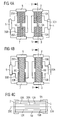
- FIGS. 1A to 1F show various views in plan view Layers of a device according to the invention, in which interconnection structures or internal electrodes are arranged. These figures each show the interconnection structure or internal electrodes disposed in the respective layer are and additionally for the sake of clarity and around the relative arrangement of the various electrical Clarify structures in the component, including the internal electrodes, each arranged in underlying layers are. Between layers in which internal electrodes or interconnection structures are arranged, respectively Any number of ceramic layers may be arranged, in which No internal electrodes or interconnection structures available are.
- FIGS. 1A to 1F show a sequence of FIGS Layers from top to bottom in the main body of the device, beginning with FIG. 1A and ending with FIG. 1F. this It can be seen from FIGS.
- an inner electrode 30, the electrically conductive with two outer contact layers. 5 and 4 is connected, overlapped with four electrode stacks, namely the electrode stack 10, consisting of the internal electrodes 10A and 10B connected to the outer contact layer 2, the electrode stack 15, consisting of the internal electrodes 15A and 15B in contact with the outer contact layer 3, the Electrode stack 20 of the inner electrodes 20A and 20B with the outer contact surface 7 and the electrode stack 25, the from the electrode layers 25A, 25B and the contact layer 6 consists.
- the electrode stacks 10 and 15 are electrically conductive via two meander-shaped interconnection structures 5A and 5B connected.
- the other two electrode stacks 25 and 20 are also over two meandering interconnection structures 5C and 5D interconnected.
- the meandering Interconnection structures have a particularly high inductance on. But are also possible differently shaped Interconnection structures, e.g. in the form of stripes.
- This Component according to the invention has two planes of symmetry on, a plane of symmetry 300 perpendicular to the ceramic Layers, which are drawn in all supervisory figures 1A to 1 F. is and one parallel to a ceramic layer extending symmetry plane 200, which is shown in Figure 1G is. These two planes of symmetry each form the interconnection structures and the internal electrodes from each other.
- FIG. 1G shows a cross section through which A in FIG. 1A designated section. It can be seen that the electrode stack 10 and 15 between the two the electrode stacks connecting meander-shaped interconnection structures 5A and 5B are arranged and the plane of symmetry 200 z. B. the interconnect structure 5A to the interconnection structure 5B and the inner electrode 15A images on the inner electrode 15B.
- FIG. 2 shows another embodiment in plan view a device according to the invention, in which, in contrast to in FIG. 1A to 1G, the electrode 30 in FIG two electrodes 30A and 30B is divided, each only overlap with two electrode stacks so that another internal Interconnection results. Only the two are top interconnect structures 5A and 5C, but not the respectively analogous interconnection structures in the lower area of the device.
- FIG. 3 shows an equivalent circuit diagram of the electrical component shown in FIG. 2 in plan view.
- the ⁇ filters shown in FIG. 3 can be realized. This results in each case a parallel connection of a capacitor effect 35 and a varistor effect 40, wherein additionally due to the two interconnection structures 5A, 5B and 5C, 5D, the parallel circuit of the capacitor and varistor effect is interconnected, wherein additionally a parallel connection of the resistors 5C and 5D or 5A and 5B result.
- the resistors are realized particularly advantageously by the meander-shaped interconnection structures shown, for example, in FIGS. 1A and 1F. It is also possible, however, to provide other forms for the interconnection structures, for example strips, and to form these from a material which has a high electrical resistance, for example RuO 2 .
- FIGS. 4A and 4B show plan views of further variants a component according to the invention, in which the Electrode stacks 10 and 15 of two differently shaped Wiring structures 5A and 5B electrically conductive get connected.
- the Interconnection structures as strips with straight course formed, wherein the interconnection structure 5A a has smaller width than the interconnect structure 5B.
- Figure 4C shows a cross-section through that with V in the figure 4A designated section. It can be seen that the strip-shaped interconnection structures 5 A and 5 B and z. B. the internal electrodes 15A, 15B by means of a plane of symmetry 200 can be imaged on each other.
- FIG. 5 shows another embodiment of a device according to the invention electrical component in cross section, the two Interconnection structures 5A and 5B as layer areas formed opposite surfaces of the body are.
- FIG. 6 shows another advantageous variant of a device according to the invention Component in the supervision of the interconnection structures 5A and 5C. It can be seen that this Interconnection structures 5A and 5C each that area cover in which the electrode 30A with the electrodes 15A and 10A and the electrode 30B with the electrodes 25A and 20A, respectively overlaps. If at least one or better still two Interconnection structures in this form two Connect electrode stacks together, these can be Electrode stack particularly advantageous over a Shield the board on which the component is mounted can. This has the consequence that the influence of the component position strong on the electrical properties of the device is reduced.
- Figure 7 shows an advantageous arrangement of a variant an electrical component according to the invention on a Substrate 100. It can be seen that the interconnection structure 5B between the substrate, the circuit board 100 and the Internal electrode stacks 10 and 15 is arranged. Through this special arrangement comes a particularly good shielding Internal electrode stacks 10 and 15 with respect to the substrate 100 conditions.
- the device 1 according to the invention can order 180 ° are rotated about the plane of symmetry 200, in which case the Interconnection structure 5A between the board 100 and the internal electrode stacks 10 and 15 would be arranged. Also at one Such rotated by 180 ° positioning can at similar to an electrical component according to the invention electrical properties are expected as in the in FIG 7 arrangement shown.
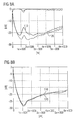
- Figure 8A shows the influence of the position of a conventional component with only one interconnect structure and no symmetry levels in the main body relative to a circuit board on the Damping behavior of the component.
- the component is as ⁇ filter executed.
- the two labeled 110 and 120 respectively Lines show the different damping behavior of the component when it is rotated 180 ° about its longitudinal axis and mounted on a circuit board. It can be seen that the different by 180 ° orientations of the component a great influence on the damping behavior of the conventional Have ⁇ filters.
- FIG. 8B shows the damping behavior of a device according to the invention ⁇ filters, in which two interconnection structures two electrode stacks Interconnect internally and in addition the two planes of symmetry are present, e.g. in Fig. 1A to 1G.
- the lines labeled 110 and 120, respectively respectively In doing so, the damping behavior is reversed by 180 ° for two the longitudinal axis rotated positions of the component on the board at. It can be clearly seen that the two different Positions in components according to the invention only show a small influence on the damping behavior.
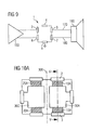
- Figure 9 shows a circuit in which an inventive electrical component 1 between an amplifier 150 and a noise sensitive device 160, such as a Speaker is switched.
- the amplifier 150 and the interference-sensitive Device 160 are via leads 170, 180th connected, wherein between the leads, the inventive Component 1 is connected.
- the outer contact layers 2, 3, 4, 5, 6 and 7 of the electrical component according to the invention refer to those in Figures 2 and 3 shown outer contact layers.
- the outer contact layer 5 is connected to the earth.
- Both high-frequency interference as for example in mobile devices over the Carrier frequency of some 100 to 10,000 MHz occur as also electrostatic discharges, which short-term pulses can generate high voltages through the device 1 safely before the device 160 are discharged to earth, wherein the useful signals, in the example of Figure 9 speech signals with a few kHz unhindered from the amplifier 150 to the device 160 can go through.
- the invention is possible with respect to the number of interconnection structures with each other connected electrode stack possible.
- Such a device has due to the shield of the Internal electrodes of the first and second electrode stack by two internal electrodes of the third electrode stack also a reduced influence of the positioning of the Component on the electrical properties in an outer Circuit environment (see, e.g., Figures 10A to 10C).
- the device is symmetrical with respect to the at least one interconnection structure and internal electrodes formed to a first level and a second level, the first plane being parallel and the second plane being vertical extends to a ceramic layer.
- the at least one interconnection structure is formed as a structured layer on the ceramic layers.
- Such an embodiment has the advantage that the interconnection structures can be produced particularly easily on the ceramic layers, for example by means of screen printing.
- the interconnection structures can be generated from conductive pastes.
- the interconnection structures can contain silver, palladium, platinum, copper, nickel or an alloy of silver and palladium or of silver and platinum, similar to the internal electrodes. Interconnection structures produced from such metals or metal alloys enable low-resistance interconnections.
- the interconnection structures to contain RuO 2 , Bi 2 Ru 2 O 7 , C, Ti 2 N or LaB 6 .
- At least two interconnection structures be present, the two electrode stacks with each other connect, so that an internal interconnection results.
- a first and second interconnect structure be present, which are formed so that they from above or At the bottom, at least the area in which the two electrode stacks overlap with the third electrode stack, covering.
- a result is particularly advantageous double shielding of the inner electrodes of the first and second Electrode stack through the inner electrodes of the third Electrode stack and wiring structures.
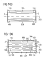
- 10A to 10C show a device according to the invention in Cross section and in the supervision.
- Fig. 10A shows in plan view two internal electrodes 30A, 30C of two third electrode stacks, each with the internal electrodes 10A, 15A and 20A, 25A of first and second, respectively Overlap electrode stacks.
- Figs. 10B and 10C respectively show Cross sections through two different variants of the Component through the designated V in Fig. 10A section. Both variants have the plan view shown in FIG. 10A and differ in the number of interconnection structures 5A, 5B, and the number of internal electrodes each Electrode stack can be seen as in the cross sections. It It can be seen that in Fig. 10B, two internal electrodes 30A, 30B a third electrode stack are arranged so that the Internal electrodes 15A, 15B and 10A, 10B disposed between them are.
- Fig. 10C shows a larger number of Inner selector electrodes per electrode stack, where additionally two Interconnection structures 5A, 5B are present and the interconnection structures and the internal electrodes of the electrode stack 10, 10A, 10B, 10C and the internal electrodes of the Electrode stack 15, 15A, 15B, 15C between the two outermost Internal electrodes 30A, 30F of the third electrode stack are arranged.
- both variants have the planes of symmetry 200 and 300 on.
Landscapes
- Engineering & Computer Science (AREA)
- Power Engineering (AREA)
- Microelectronics & Electronic Packaging (AREA)
- Manufacturing & Machinery (AREA)
- Physics & Mathematics (AREA)
- Electromagnetism (AREA)
- Fixed Capacitors And Capacitor Manufacturing Machines (AREA)
- Ceramic Capacitors (AREA)
- Connection Of Batteries Or Terminals (AREA)
- Coils Or Transformers For Communication (AREA)
- Thermistors And Varistors (AREA)
Priority Applications (1)
| Application Number | Priority Date | Filing Date | Title |
|---|---|---|---|
| EP10173301.2A EP2246866B1 (fr) | 2003-12-03 | 2004-12-03 | Composant électrique et agencement de circuit |
Applications Claiming Priority (2)
| Application Number | Priority Date | Filing Date | Title |
|---|---|---|---|
| DE10356498 | 2003-12-03 | ||
| DE10356498A DE10356498A1 (de) | 2003-12-03 | 2003-12-03 | Elektrisches Bauelement und Schaltungsanordnung |
Related Child Applications (2)
| Application Number | Title | Priority Date | Filing Date |
|---|---|---|---|
| EP10173301.2A Division EP2246866B1 (fr) | 2003-12-03 | 2004-12-03 | Composant électrique et agencement de circuit |
| EP10173301.2 Division-Into | 2010-08-18 |
Publications (3)
| Publication Number | Publication Date |
|---|---|
| EP1538641A2 true EP1538641A2 (fr) | 2005-06-08 |
| EP1538641A3 EP1538641A3 (fr) | 2007-06-06 |
| EP1538641B1 EP1538641B1 (fr) | 2011-05-18 |
Family
ID=34442423
Family Applications (2)
| Application Number | Title | Priority Date | Filing Date |
|---|---|---|---|
| EP04028710A Expired - Lifetime EP1538641B1 (fr) | 2003-12-03 | 2004-12-03 | Composant électrique et agencement de circuit |
| EP10173301.2A Expired - Lifetime EP2246866B1 (fr) | 2003-12-03 | 2004-12-03 | Composant électrique et agencement de circuit |
Family Applications After (1)
| Application Number | Title | Priority Date | Filing Date |
|---|---|---|---|
| EP10173301.2A Expired - Lifetime EP2246866B1 (fr) | 2003-12-03 | 2004-12-03 | Composant électrique et agencement de circuit |
Country Status (4)
| Country | Link |
|---|---|
| EP (2) | EP1538641B1 (fr) |
| AT (1) | ATE510289T1 (fr) |
| DE (1) | DE10356498A1 (fr) |
| ES (1) | ES2366782T3 (fr) |
Cited By (3)
| Publication number | Priority date | Publication date | Assignee | Title |
|---|---|---|---|---|
| WO2008135466A1 (fr) * | 2007-05-03 | 2008-11-13 | Epcos Ag | Composant électrique à plusieurs couches avec structure de blindage sans contact électrique |
| US8730645B2 (en) | 2007-07-06 | 2014-05-20 | Epcos Ag | Multilayer electrical component |
| EP2833372A1 (fr) * | 2013-07-31 | 2015-02-04 | Forschungszentrum Jülich GmbH | Résistance ayant une capacité parasitaire réduite |
Families Citing this family (1)
| Publication number | Priority date | Publication date | Assignee | Title |
|---|---|---|---|---|
| DE102009049077A1 (de) | 2009-10-12 | 2011-04-14 | Epcos Ag | Elektrisches Vielschichtbauelement und Schaltungsanordnung |
Citations (2)
| Publication number | Priority date | Publication date | Assignee | Title |
|---|---|---|---|---|
| JPH1097954A (ja) | 1996-09-24 | 1998-04-14 | Taiyo Yuden Co Ltd | 積層チップ形のcrフィルタおよびcrフィルタアレイ |
| DE10144364A1 (de) | 2001-09-10 | 2003-04-03 | Epcos Ag | Elektrisches Vielschichtbauelement |
Family Cites Families (6)
| Publication number | Priority date | Publication date | Assignee | Title |
|---|---|---|---|---|
| JPH08124800A (ja) * | 1994-10-27 | 1996-05-17 | Tdk Corp | コンデンサアレイ |
| US5815367A (en) * | 1996-03-11 | 1998-09-29 | Murata Manufacturing Co., Ltd. | Layered capacitors having an internal inductor element |
| JP2000058382A (ja) * | 1998-08-14 | 2000-02-25 | Sumitomo Metal Ind Ltd | チップ型cr部品 |
| JP2000124068A (ja) * | 1998-10-16 | 2000-04-28 | Matsushita Electric Ind Co Ltd | 積層型ノイズフィルタ |
| DE10064447C2 (de) * | 2000-12-22 | 2003-01-02 | Epcos Ag | Elektrisches Vielschichtbauelement und Entstörschaltung mit dem Bauelement |
| DE10224565A1 (de) * | 2002-06-03 | 2003-12-18 | Epcos Ag | Elektrisches Vielschichtbauelement und Schaltungsanordnung |
-
2003
- 2003-12-03 DE DE10356498A patent/DE10356498A1/de not_active Ceased
-
2004
- 2004-12-03 EP EP04028710A patent/EP1538641B1/fr not_active Expired - Lifetime
- 2004-12-03 AT AT04028710T patent/ATE510289T1/de active
- 2004-12-03 EP EP10173301.2A patent/EP2246866B1/fr not_active Expired - Lifetime
- 2004-12-03 ES ES04028710T patent/ES2366782T3/es not_active Expired - Lifetime
Patent Citations (2)
| Publication number | Priority date | Publication date | Assignee | Title |
|---|---|---|---|---|
| JPH1097954A (ja) | 1996-09-24 | 1998-04-14 | Taiyo Yuden Co Ltd | 積層チップ形のcrフィルタおよびcrフィルタアレイ |
| DE10144364A1 (de) | 2001-09-10 | 2003-04-03 | Epcos Ag | Elektrisches Vielschichtbauelement |
Cited By (4)
| Publication number | Priority date | Publication date | Assignee | Title |
|---|---|---|---|---|
| WO2008135466A1 (fr) * | 2007-05-03 | 2008-11-13 | Epcos Ag | Composant électrique à plusieurs couches avec structure de blindage sans contact électrique |
| US8179210B2 (en) | 2007-05-03 | 2012-05-15 | Epcos Ag | Electrical multilayer component with shielding and resistance structures |
| US8730645B2 (en) | 2007-07-06 | 2014-05-20 | Epcos Ag | Multilayer electrical component |
| EP2833372A1 (fr) * | 2013-07-31 | 2015-02-04 | Forschungszentrum Jülich GmbH | Résistance ayant une capacité parasitaire réduite |
Also Published As
| Publication number | Publication date |
|---|---|
| DE10356498A1 (de) | 2005-07-07 |
| ATE510289T1 (de) | 2011-06-15 |
| EP1538641A3 (fr) | 2007-06-06 |
| EP1538641B1 (fr) | 2011-05-18 |
| EP2246866A1 (fr) | 2010-11-03 |
| EP2246866B1 (fr) | 2017-10-25 |
| ES2366782T3 (es) | 2011-10-25 |
Similar Documents
| Publication | Publication Date | Title |
|---|---|---|
| DE69830885T2 (de) | Vielschichtkondensator | |
| EP2143117B1 (fr) | Composant électrique multicouche comportant une structure de blindage sans contact électrique | |
| DE19628890B4 (de) | LC-Filter | |
| DE69805391T2 (de) | Mehrschichtiger Hochfrequenzbauteil | |
| DE4008507C2 (de) | Laminiertes LC-Filter | |
| EP1606831B1 (fr) | Composant multicouche electrique | |
| DE10019229A1 (de) | Mehrschichtkondensator | |
| DE10046910A1 (de) | Halbleitervorrichtung | |
| EP1369880B1 (fr) | Composant électrique multicouche et circuit | |
| DE19716896A1 (de) | LC-Filter | |
| DE69823637T2 (de) | Laminat-Varistor | |
| EP1369881B1 (fr) | Composant électrique multicouche | |
| DE102004010001A1 (de) | Elektrisches Bauelement und schaltungsanordnung mit dem Bauelement | |
| DE4342818C2 (de) | Zusammengesetztes elektronisches Bauteil | |
| DE102005028498B4 (de) | Elektrisches Vielschichtbauelement | |
| EP2246866B1 (fr) | Composant électrique et agencement de circuit | |
| EP1880399B1 (fr) | Element de traversee electrique | |
| EP1391898B1 (fr) | Composant électrique multicouche | |
| DE102004016146A1 (de) | Elektrische Funktionseinheit | |
| DE102004058410B4 (de) | Vielschichtbauelement mit ESD-Schutzelementen | |
| DE60036238T2 (de) | Vielschicht-Keramikkondensator für dreidimensionale Montage | |
| DE19958484A1 (de) | Mehrfach-Filter | |
| EP1560235A2 (fr) | Composant multicouche électrique | |
| DE102007021950A1 (de) | Filterschaltung und Filterelement | |
| DE10037000C2 (de) | Elektronische Schaltung mit Tiefpasscharakteristik und Verfahren zu ihrer Herstellung |
Legal Events
| Date | Code | Title | Description |
|---|---|---|---|
| PUAI | Public reference made under article 153(3) epc to a published international application that has entered the european phase |
Free format text: ORIGINAL CODE: 0009012 |
|
| AK | Designated contracting states |
Kind code of ref document: A2 Designated state(s): AT BE BG CH CY CZ DE DK EE ES FI FR GB GR HU IE IS IT LI LT LU MC NL PL PT RO SE SI SK TR |
|
| AX | Request for extension of the european patent |
Extension state: AL BA HR LV MK YU |
|
| PUAL | Search report despatched |
Free format text: ORIGINAL CODE: 0009013 |
|
| AK | Designated contracting states |
Kind code of ref document: A3 Designated state(s): AT BE BG CH CY CZ DE DK EE ES FI FR GB GR HU IE IS IT LI LT LU MC NL PL PT RO SE SI SK TR |
|
| AX | Request for extension of the european patent |
Extension state: AL BA HR LV MK YU |
|
| RIC1 | Information provided on ipc code assigned before grant |
Ipc: H03H 7/01 20060101ALN20070503BHEP Ipc: H01G 4/40 20060101AFI20050310BHEP Ipc: H01C 13/02 20060101ALI20070503BHEP |
|
| 17P | Request for examination filed |
Effective date: 20071106 |
|
| AKX | Designation fees paid |
Designated state(s): AT BE BG CH CY CZ DE DK EE ES FI FR GB GR HU IE IS IT LI LT LU MC NL PL PT RO SE SI SK TR |
|
| 17Q | First examination report despatched |
Effective date: 20100301 |
|
| GRAP | Despatch of communication of intention to grant a patent |
Free format text: ORIGINAL CODE: EPIDOSNIGR1 |
|
| GRAS | Grant fee paid |
Free format text: ORIGINAL CODE: EPIDOSNIGR3 |
|
| GRAA | (expected) grant |
Free format text: ORIGINAL CODE: 0009210 |
|
| AK | Designated contracting states |
Kind code of ref document: B1 Designated state(s): AT BE BG CH CY CZ DE DK EE ES FI FR GB GR HU IE IS IT LI LT LU MC NL PL PT RO SE SI SK TR |
|
| REG | Reference to a national code |
Ref country code: GB Ref legal event code: FG4D Free format text: NOT ENGLISH |
|
| REG | Reference to a national code |
Ref country code: CH Ref legal event code: EP |
|
| REG | Reference to a national code |
Ref country code: IE Ref legal event code: FG4D Free format text: LANGUAGE OF EP DOCUMENT: GERMAN |
|
| REG | Reference to a national code |
Ref country code: DE Ref legal event code: R096 Ref document number: 502004012518 Country of ref document: DE Effective date: 20110630 |
|
| REG | Reference to a national code |
Ref country code: NL Ref legal event code: VDEP Effective date: 20110518 |
|
| REG | Reference to a national code |
Ref country code: ES Ref legal event code: FG2A Ref document number: 2366782 Country of ref document: ES Kind code of ref document: T3 Effective date: 20111025 |
|
| PG25 | Lapsed in a contracting state [announced via postgrant information from national office to epo] |
Ref country code: PT Free format text: LAPSE BECAUSE OF FAILURE TO SUBMIT A TRANSLATION OF THE DESCRIPTION OR TO PAY THE FEE WITHIN THE PRESCRIBED TIME-LIMIT Effective date: 20110919 Ref country code: SE Free format text: LAPSE BECAUSE OF FAILURE TO SUBMIT A TRANSLATION OF THE DESCRIPTION OR TO PAY THE FEE WITHIN THE PRESCRIBED TIME-LIMIT Effective date: 20110518 Ref country code: LT Free format text: LAPSE BECAUSE OF FAILURE TO SUBMIT A TRANSLATION OF THE DESCRIPTION OR TO PAY THE FEE WITHIN THE PRESCRIBED TIME-LIMIT Effective date: 20110518 |
|
| PG25 | Lapsed in a contracting state [announced via postgrant information from national office to epo] |
Ref country code: GR Free format text: LAPSE BECAUSE OF FAILURE TO SUBMIT A TRANSLATION OF THE DESCRIPTION OR TO PAY THE FEE WITHIN THE PRESCRIBED TIME-LIMIT Effective date: 20110819 Ref country code: IS Free format text: LAPSE BECAUSE OF FAILURE TO SUBMIT A TRANSLATION OF THE DESCRIPTION OR TO PAY THE FEE WITHIN THE PRESCRIBED TIME-LIMIT Effective date: 20110918 Ref country code: CY Free format text: LAPSE BECAUSE OF FAILURE TO SUBMIT A TRANSLATION OF THE DESCRIPTION OR TO PAY THE FEE WITHIN THE PRESCRIBED TIME-LIMIT Effective date: 20110518 Ref country code: SI Free format text: LAPSE BECAUSE OF FAILURE TO SUBMIT A TRANSLATION OF THE DESCRIPTION OR TO PAY THE FEE WITHIN THE PRESCRIBED TIME-LIMIT Effective date: 20110518 Ref country code: FI Free format text: LAPSE BECAUSE OF FAILURE TO SUBMIT A TRANSLATION OF THE DESCRIPTION OR TO PAY THE FEE WITHIN THE PRESCRIBED TIME-LIMIT Effective date: 20110518 |
|
| REG | Reference to a national code |
Ref country code: IE Ref legal event code: FD4D |
|
| PG25 | Lapsed in a contracting state [announced via postgrant information from national office to epo] |
Ref country code: NL Free format text: LAPSE BECAUSE OF FAILURE TO SUBMIT A TRANSLATION OF THE DESCRIPTION OR TO PAY THE FEE WITHIN THE PRESCRIBED TIME-LIMIT Effective date: 20110518 |
|
| PG25 | Lapsed in a contracting state [announced via postgrant information from national office to epo] |
Ref country code: IE Free format text: LAPSE BECAUSE OF FAILURE TO SUBMIT A TRANSLATION OF THE DESCRIPTION OR TO PAY THE FEE WITHIN THE PRESCRIBED TIME-LIMIT Effective date: 20110518 Ref country code: EE Free format text: LAPSE BECAUSE OF FAILURE TO SUBMIT A TRANSLATION OF THE DESCRIPTION OR TO PAY THE FEE WITHIN THE PRESCRIBED TIME-LIMIT Effective date: 20110518 Ref country code: CZ Free format text: LAPSE BECAUSE OF FAILURE TO SUBMIT A TRANSLATION OF THE DESCRIPTION OR TO PAY THE FEE WITHIN THE PRESCRIBED TIME-LIMIT Effective date: 20110518 |
|
| PG25 | Lapsed in a contracting state [announced via postgrant information from national office to epo] |
Ref country code: PL Free format text: LAPSE BECAUSE OF FAILURE TO SUBMIT A TRANSLATION OF THE DESCRIPTION OR TO PAY THE FEE WITHIN THE PRESCRIBED TIME-LIMIT Effective date: 20110518 Ref country code: RO Free format text: LAPSE BECAUSE OF FAILURE TO SUBMIT A TRANSLATION OF THE DESCRIPTION OR TO PAY THE FEE WITHIN THE PRESCRIBED TIME-LIMIT Effective date: 20110518 Ref country code: SK Free format text: LAPSE BECAUSE OF FAILURE TO SUBMIT A TRANSLATION OF THE DESCRIPTION OR TO PAY THE FEE WITHIN THE PRESCRIBED TIME-LIMIT Effective date: 20110518 Ref country code: DK Free format text: LAPSE BECAUSE OF FAILURE TO SUBMIT A TRANSLATION OF THE DESCRIPTION OR TO PAY THE FEE WITHIN THE PRESCRIBED TIME-LIMIT Effective date: 20110518 |
|
| PLBE | No opposition filed within time limit |
Free format text: ORIGINAL CODE: 0009261 |
|
| STAA | Information on the status of an ep patent application or granted ep patent |
Free format text: STATUS: NO OPPOSITION FILED WITHIN TIME LIMIT |
|
| 26N | No opposition filed |
Effective date: 20120221 |
|
| REG | Reference to a national code |
Ref country code: DE Ref legal event code: R097 Ref document number: 502004012518 Country of ref document: DE Effective date: 20120221 |
|
| BERE | Be: lapsed |
Owner name: EPCOS A.G. Effective date: 20111231 |
|
| PG25 | Lapsed in a contracting state [announced via postgrant information from national office to epo] |
Ref country code: MC Free format text: LAPSE BECAUSE OF NON-PAYMENT OF DUE FEES Effective date: 20111231 |
|
| REG | Reference to a national code |
Ref country code: CH Ref legal event code: PL |
|
| PG25 | Lapsed in a contracting state [announced via postgrant information from national office to epo] |
Ref country code: LI Free format text: LAPSE BECAUSE OF NON-PAYMENT OF DUE FEES Effective date: 20111231 Ref country code: BE Free format text: LAPSE BECAUSE OF NON-PAYMENT OF DUE FEES Effective date: 20111231 Ref country code: CH Free format text: LAPSE BECAUSE OF NON-PAYMENT OF DUE FEES Effective date: 20111231 |
|
| REG | Reference to a national code |
Ref country code: AT Ref legal event code: MM01 Ref document number: 510289 Country of ref document: AT Kind code of ref document: T Effective date: 20111203 |
|
| PG25 | Lapsed in a contracting state [announced via postgrant information from national office to epo] |
Ref country code: LU Free format text: LAPSE BECAUSE OF NON-PAYMENT OF DUE FEES Effective date: 20111203 |
|
| PG25 | Lapsed in a contracting state [announced via postgrant information from national office to epo] |
Ref country code: BG Free format text: LAPSE BECAUSE OF FAILURE TO SUBMIT A TRANSLATION OF THE DESCRIPTION OR TO PAY THE FEE WITHIN THE PRESCRIBED TIME-LIMIT Effective date: 20110818 Ref country code: AT Free format text: LAPSE BECAUSE OF NON-PAYMENT OF DUE FEES Effective date: 20111203 |
|
| PG25 | Lapsed in a contracting state [announced via postgrant information from national office to epo] |
Ref country code: TR Free format text: LAPSE BECAUSE OF FAILURE TO SUBMIT A TRANSLATION OF THE DESCRIPTION OR TO PAY THE FEE WITHIN THE PRESCRIBED TIME-LIMIT Effective date: 20110518 |
|
| PG25 | Lapsed in a contracting state [announced via postgrant information from national office to epo] |
Ref country code: HU Free format text: LAPSE BECAUSE OF FAILURE TO SUBMIT A TRANSLATION OF THE DESCRIPTION OR TO PAY THE FEE WITHIN THE PRESCRIBED TIME-LIMIT Effective date: 20110518 |
|
| PGFP | Annual fee paid to national office [announced via postgrant information from national office to epo] |
Ref country code: GB Payment date: 20131217 Year of fee payment: 10 |
|
| PGFP | Annual fee paid to national office [announced via postgrant information from national office to epo] |
Ref country code: ES Payment date: 20131216 Year of fee payment: 10 Ref country code: IT Payment date: 20131217 Year of fee payment: 10 |
|
| GBPC | Gb: european patent ceased through non-payment of renewal fee |
Effective date: 20141203 |
|
| PG25 | Lapsed in a contracting state [announced via postgrant information from national office to epo] |
Ref country code: GB Free format text: LAPSE BECAUSE OF NON-PAYMENT OF DUE FEES Effective date: 20141203 |
|
| REG | Reference to a national code |
Ref country code: FR Ref legal event code: PLFP Year of fee payment: 12 |
|
| PG25 | Lapsed in a contracting state [announced via postgrant information from national office to epo] |
Ref country code: IT Free format text: LAPSE BECAUSE OF NON-PAYMENT OF DUE FEES Effective date: 20141203 |
|
| REG | Reference to a national code |
Ref country code: ES Ref legal event code: FD2A Effective date: 20160127 |
|
| PG25 | Lapsed in a contracting state [announced via postgrant information from national office to epo] |
Ref country code: ES Free format text: LAPSE BECAUSE OF NON-PAYMENT OF DUE FEES Effective date: 20141204 |
|
| REG | Reference to a national code |
Ref country code: FR Ref legal event code: PLFP Year of fee payment: 13 |
|
| REG | Reference to a national code |
Ref country code: FR Ref legal event code: PLFP Year of fee payment: 14 |
|
| REG | Reference to a national code |
Ref country code: DE Ref legal event code: R082 Ref document number: 502004012518 Country of ref document: DE Representative=s name: EPPING HERMANN FISCHER PATENTANWALTSGESELLSCHA, DE Ref country code: DE Ref legal event code: R081 Ref document number: 502004012518 Country of ref document: DE Owner name: TDK ELECTRONICS AG, DE Free format text: FORMER OWNER: EPCOS AG, 81669 MUENCHEN, DE |
|
| PGFP | Annual fee paid to national office [announced via postgrant information from national office to epo] |
Ref country code: FR Payment date: 20191218 Year of fee payment: 16 |
|
| PG25 | Lapsed in a contracting state [announced via postgrant information from national office to epo] |
Ref country code: FR Free format text: LAPSE BECAUSE OF NON-PAYMENT OF DUE FEES Effective date: 20201231 |
|
| P01 | Opt-out of the competence of the unified patent court (upc) registered |
Effective date: 20230521 |
|
| PGFP | Annual fee paid to national office [announced via postgrant information from national office to epo] |
Ref country code: DE Payment date: 20231218 Year of fee payment: 20 |
|
| REG | Reference to a national code |
Ref country code: DE Ref legal event code: R071 Ref document number: 502004012518 Country of ref document: DE |