EP1548802B1 - Dispositif conducteur de lumiere - Google Patents
Dispositif conducteur de lumiere Download PDFInfo
- Publication number
- EP1548802B1 EP1548802B1 EP03741212A EP03741212A EP1548802B1 EP 1548802 B1 EP1548802 B1 EP 1548802B1 EP 03741212 A EP03741212 A EP 03741212A EP 03741212 A EP03741212 A EP 03741212A EP 1548802 B1 EP1548802 B1 EP 1548802B1
- Authority
- EP
- European Patent Office
- Prior art keywords
- light
- face
- light emitting
- optical fiber
- glass rod
- Prior art date
- Legal status (The legal status is an assumption and is not a legal conclusion. Google has not performed a legal analysis and makes no representation as to the accuracy of the status listed.)
- Expired - Lifetime
Links
Images


Classifications
-
- G—PHYSICS
- G03—PHOTOGRAPHY; CINEMATOGRAPHY; ANALOGOUS TECHNIQUES USING WAVES OTHER THAN OPTICAL WAVES; ELECTROGRAPHY; HOLOGRAPHY
- G03F—PHOTOMECHANICAL PRODUCTION OF TEXTURED OR PATTERNED SURFACES, e.g. FOR PRINTING, FOR PROCESSING OF SEMICONDUCTOR DEVICES; MATERIALS THEREFOR; ORIGINALS THEREFOR; APPARATUS SPECIALLY ADAPTED THEREFOR
- G03F7/00—Photomechanical, e.g. photolithographic, production of textured or patterned surfaces, e.g. printing surfaces; Materials therefor, e.g. comprising photoresists; Apparatus specially adapted therefor
- G03F7/70—Microphotolithographic exposure; Apparatus therefor
- G03F7/70008—Production of exposure light, i.e. light sources
-
- G—PHYSICS
- G02—OPTICS
- G02B—OPTICAL ELEMENTS, SYSTEMS OR APPARATUS
- G02B6/00—Light guides; Structural details of arrangements comprising light guides and other optical elements, e.g. couplings
- G02B6/04—Light guides; Structural details of arrangements comprising light guides and other optical elements, e.g. couplings formed by bundles of fibres
-
- G—PHYSICS
- G02—OPTICS
- G02B—OPTICAL ELEMENTS, SYSTEMS OR APPARATUS
- G02B6/00—Light guides; Structural details of arrangements comprising light guides and other optical elements, e.g. couplings
- G02B6/10—Light guides; Structural details of arrangements comprising light guides and other optical elements, e.g. couplings of the optical waveguide type
-
- G—PHYSICS
- G02—OPTICS
- G02B—OPTICAL ELEMENTS, SYSTEMS OR APPARATUS
- G02B6/00—Light guides; Structural details of arrangements comprising light guides and other optical elements, e.g. couplings
- G02B6/24—Coupling light guides
- G02B6/42—Coupling light guides with opto-electronic elements
- G02B6/4298—Coupling light guides with opto-electronic elements coupling with non-coherent light sources and/or radiation detectors, e.g. lamps, incandescent bulbs, scintillation chambers
-
- G—PHYSICS
- G02—OPTICS
- G02B—OPTICAL ELEMENTS, SYSTEMS OR APPARATUS
- G02B6/00—Light guides; Structural details of arrangements comprising light guides and other optical elements, e.g. couplings
- G02B6/24—Coupling light guides
- G02B6/42—Coupling light guides with opto-electronic elements
- G02B6/4201—Packages, e.g. shape, construction, internal or external details
- G02B6/4204—Packages, e.g. shape, construction, internal or external details the coupling comprising intermediate optical elements, e.g. lenses, holograms
- G02B6/4206—Optical features
Definitions
- the present invention concerns a light guiding device that is used to perform exposure for removal of unnecessary resist on peripheral parts of a semiconductor wafer.
- the light emitting from the light guiding device be shaped to have a cross section of rectangular shape and that the illuminance be made uniform across the entire cross section of the emitting light.
- US 5,229,811 discloses a light guiding device for exposure of peripheral parts of a semiconductor wafer, comprising an optical fibre bundle.
- EP 0 788 032 discloses a light guiding device used for edge bead removal comprising an optical fibre bundle and an exit optical system comprising lenses.
- the present invention has been made to resolve the above issue, and an object thereof is to provide a light guiding device, which shapes the cross section of light, emitting from a light guide fiber, to a rectangular shape and makes uniform the illuminance across the entire cross section of the emitting light without decreasing the light amount of the emitting light.
- this invention provides in a light guiding device used for exposure of peripheral parts of a semiconductor wafer, a light guiding device, comprising: an optical fiber bundle, formed by bundling together a plurality of optical fibers and having a first light incidence end face and a first light emitting end face; a glass rod, having a second light incidence end face and a second light emitting end face and making uniform the cross section of light emitting from the second light emitting end face by taking in, from the second light incidence end face, the light emitting from the first light emitting end face of the optical fiber bundle and guiding this light to the second light emitting end face; and a glass rod holding member, which fixes the glass rod to a light emitting end face side front end part of the optical fiber bundle so that the second light incidence end face of the glass rod opposes the first light emitting end face of the optical fiber bundle; the second light emitting end face of the glass rod having a rectangular shape.
- the glass rod takes in the light emitting from the optical fiber bundle and makes the illuminance uniform across the entire cross section of the emitting light. Also, since the second light emitting end face of the glass rod has a rectangular shape, the emitting light from the glass rod is shaped to be rectangular in cross section. The light thus does not have to be shaped by applying an aperture member and blocking the outer rim of the cross section of the emitting light. Consequently, the light that is guided by the optical fiber bundle can be illuminated onto peripheral parts of a semiconductor wafer without decrease of the light amount.
- the glass rod preferably satisfies the relationships expressed by the following formulae (A) and (B).
- L ⁇ d 2 ⁇ 1 tan ⁇ n ⁇ sin ⁇ n ⁇ ⁇ sin ⁇ L[mm]: length of the glass rod d[mm]: length of the diagonal of the second light emitting end face of the glass rod n: refractive index of air n': refractive index of the glass rod ⁇ : maximum angle of emit from the optical fiber into air ⁇ ' : angle of refraction of light, which has emited from the optical fiber at the maximum emit angle, upon incidence onto the second light incidence end face
- the maximum emitted angle component among the emitting light from the optical fiber that enters the glass rod via the central axis, is totally reflected at least once at the boundary surface (interface between the glass rod and a cladding or ambient air) of the glass rod.
- a sleeve member which covers the light emitting end face side front end part of the optical fiber bundle, to be equipped and for the glass rod holding member to be detachably mounted to the sleeve member.
- the glass rod holding member can then be removed from the sleeve member, exchange and washing of the glass rod are facilitated.
- the plurality of optical fibers prefferably be adhered to each other by an adhesive agent at the light emitting end face side front end part of the optical fiber bundle.
- the shape of the light emitting end face side front end part can be maintained regardless of the shape of the optical fiber bundle. Also, the density of the core end faces at the first light emitting end face of the optical fiber bundle is made high and dark parts (parts besides the core end faces) are lessened. The light amount density at the first light emitting end face is thereby increased.
- the first light emitting end face of the optical fiber bundle it is preferable for the first light emitting end face of the optical fiber bundle to oppose the second light incidence end face of the glass rod across a gap.
- this invention's light guiding device is preferably equipped with a sleeve member, covering the light emitting end face side front end part of the optical fiber bundle, and a curving part holding member, which, by being fixed to the vicinity of the light emitting end face side front end part of the optical fiber bundle and to the sleeve member, maintains a state wherein the optical fiber bundle is curved in the vicinity of the front end part.
- the space occupied by the optical fiber bundle in the vicinity of the light emitting end face side front end part can be made small.
- Fig. 1 is a diagram showing the outer appearance of a light guiding device 1.
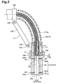
- Fig. 2 is a partial sectional view showing a region X in Fig. 1 of light guiding device 1 in enlarged manner.
- Fig. 3 is a diagram showing a light emitting end face of a light guide cable 10.
- Fig. 4 is a diagram showing a light emitting end face of an illumination head 4.
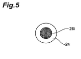
- Fig. 5 is a diagram showing the end face of a first light incidence part.
- Fig. 6 is a diagram showing the manner in which a light emitting end face side front end part of an optical fiber bundle 16 is fitted into a sleeve member 13.
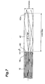
- Fig. 7 is a diagram, showing the manner in which light is totally reflected and propagated in a cross section along the length direction (cross section containing the diagonal of a light emitting end face 40o) of a glass rod 40.
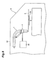
- Fig. 8 is a schematic diagram of a semiconductor wafer periphery exposure device 5 to which light guiding device 1 is applied.
- Fig. 1 is a diagram showing the outer appearance of light guiding device 1.
- Fig. 2 is a partial sectional view showing a region X in Fig. 1 of light guiding device 1 in enlarged manner.
- Light guiding device 1 is equipped, at a light emitting end face side, with a light guide cable 10, which is arranged by an optical fiber bundle 16, formed by bundling together a plurality of optical fiber cores (UV transmitting quartz fiber cores), being covered by a PVC cladding 17.
- the light guide cable 10 is branched at a light incidence end face side into a light guide cable 20 and light guide cable 30.
- Light guide cable 20 and light guide cable 30 are substantially equal in the number of cores, and by bundling together the optical fiber cores that make up these cables at the branching part, optical fiber bundle 16 of light guide cable 10 is formed.
- the branching part of this optical fiber cable is covered by a branching part outer cover 11.
- FIG. 3 is a diagram showing the light emitting end face of light guide cable 10.
- Fig. 6 is a diagram showing the manner in which the light emitting end face side front end part of optical fiber bundle 16 is fitted into sleeve member 13.
- Optical fiber bundle 16 is fixed in shape at the light emitting end face side front end part (part corresponding to a region Y shown in Fig.
- the cross-sectional shape of the light emitting end face side front end part is formed to a rectangular shape, which is 8.0mm in the lateral direction and 4.0mm in the longitudinal direction, as shown in Fig. 3 .
- the alignment of the optical fiber cores at the light emitting end face side front end part is preferably as random as possible with respect to the alignment of the optical fiber cores at the other parts. The making of the alignment of the optical fiber cores at the light emitting end face side front end part random contributes to the making uniform of the scattering of the light amounts of the light emitting from the respective optical fiber cores.
- sleeve member 13 is a cylindrical member, the overall shape of which is an elliptical column.
- the hollow part of sleeve member 13 has a rectangular cross section, which is 8.0mm in the lateral direction and 4.0mm in the longitudinal direction, and at the opening at one side, a step 13a is formed by the slight protruding of a side wall.
- the thickness of step 13a is adjusted to be of a predetermined length g.
- Optical fiber bundle 16 the light emitting end face side front end part of which is fixed by the adhesive agent, is inserted into the hollow part and thereby fitted into sleeve member 13.
- step 13a Upon fitting, step 13a latches onto a light emit end face 16o of optical fiber bundle 16 and a gap of interval g is formed between the bottom face of sleeve member 13 and light emitting end face 16o.
- optical fiber bundle 16 thus being fitted into sleeve member 13, the shape of the light emitting end face side front end part is maintained regardless of variations of the shape of optical fiber bundle 16.
- the light emitting end face side front end part being fixed by the adhesive agent, the shape is fixed even more strongly, the density of core end faces at light emitting end face 16o is made high, and dark parts (parts besides the core end faces) are lessened. The light amount density at light emitting end face 16o is thus made high.
- Sleeve member 13 is a cylindrical member, the overall shape of which is an elliptical column, and an emitting part outer cover 14, having a hollow part of elliptical columnar shape, is mounted so that the bottom face of sleeve member 13 and the bottom face of emitting part outer cover 14 are positioned on the same plane.
- the light emitting end face side front end part of optical fiber bundle 16 is covered by emitting part outer cover 14 and PVC cladding 17.
- an illumination head 4 is detachably mounted to the light emitting end face side front end part of optical fiber bundle 16.
- Illumination head 4 comprises a glass rod holding member 42, a glass rod 40, which is housed in glass rod holding member 42, and a positioning pin 44, which fixes glass rod 40, and glass rod 40 is set to oppose light emitting end face 16o of optical fiber bundle 16.
- Fig. 4 is a diagram showing a light emitting end face of illumination head 4.
- Glass rod 40 has basal faces with a rectangular shape that is 8.0mm in the lateral direction and 4.0 in the longitudinal direction and has a quadratic prism shape with a length (height) of 40.0mm.
- the basal face at one side of glass rod 40 becomes a light incidence end face 40i and the other basal face becomes a light emitting end face 40o.
- glass rod holding member 42 has a cylindrical shape and the inner periphery and outer periphery of the cross section at the front end part (glass rod housing part) are both elliptical in shape. Though the inner periphery and outer periphery of the cross section at the terminal end part (emitting part outer cover mounting part) are also elliptical, the inner peripheral diameters of the emitting part outer cover mounting part are greater than the inner peripheral diameters of the glass rod housing part.
- the major diameter of the inner periphery of the cross section is set to be longer than 8.0mm (the length of the lateral side of light emitting end face 40o of glass rod 40) and the minor diameter is set to be longer than 4.0mm (the length of the longitudinal side of light emitting end face 40o of glass rod 40).
- the length of the hollow part is set to 40.0mm (the length of glass rod 40).
- four positioning pin insertion holes 42a are formed at each of the front end part side and the terminal end part side. Glass rod 40 is housed with a degree of freedom when it is inserted into the glass rod housing part and the position of glass rod 40 is fixed by positioning pins 44 that are inserted into positioning pin insertion holes 42a. Threaded grooves may be formed at the side faces of positioning pin insertion holes 42a and positioning screws may be screwed into positioning pin insertion holes 42a in place of positioning pins 44.
- the shape and size of the inner periphery of the cross section at the emitting part outer cover mounting part are the same as those of the outer periphery of emitting part outer cover 14, and emitting part outer cover 14 is set to be fitted in the hollow part of the emitting part outer cover mounting part.
- illumination head 4 is mounted detachably to emitting part outer cover 14.
- Illumination head 4 is thus detachably mounted via illumination part outer cover 14 to sleeve member 13. Since illumination head 4 is thus made detachable, exchange and washing of glass rod 40 are facilitated.
- a step 42b is formed at the boundary part of these parts.
- this step 42b latches onto the bottom face of emitting part outer cover 14.
- glass rod 40 is inserted into the glass rod housing part, glass rod 40 is fixed so that light incidence end face 40i is positioned on the same plane as step 42b (the bottom faces of emitting part outer cover 14 and sleeve member 13).
- glass rod 40 is fixed so as to oppose light emitting end face 16o of optical fiber bundle 16 across a gap of interval g. Furthermore, by shifting the positions of positioning pins 44, the orientation of glass rod 40 is adjusted so that light incidence end face 40i can pick up the emitting light from light emitting end face 16o without leakage.
- light guide cable 10 is curved at a right angle near the front end part and this shape is held by a curving part holding member 12.
- Curving member holding part 12 is equipped and arranged with a ring 122, a ring 124, a fixing plate 126, and screws 128.
- Ring 122 is fixed at a location near the front end part of light guide cable 10.
- Ring 124 is fixed onto the outer peripheral surface of emitting part outer cover 14. That is, ring 124 is fixed to sleeve member 13 via emitting part outer cover 14.
- the respective end parts of fixing plate 126 are mounted to ring 122 and ring 124 and, after being fastened by screws 128, are fixed by an epoxy adhesive agent.
- the optical fiber cores of optical fiber bundle 16 are twisted together to provide a bend-resistant structure. For example, approximately 200 optical fiber cores are twisted together to form a sub-bundle and seven such sub-bundles are twisted together to form the optical fiber bundle.
- light guide cable 10 is thus curved at a right angle near its front end part and this shape is held by curving part holding member 12, good maintenance of the vertical illumination state of the emitting light, prevention of damage of optical fiber bundle 16 due to repeated curving, and prevention of damage due to the contacting of the front end part of light guide cable 10 with inner peripheral parts of the exposure device resulting from the front end part being in a floating state in the process of mounting the device are enabled.
- Fig. 5 is a diagram showing the end face of the first light incidence part.
- the front end face (light incidence end face 26i) of the optical fiber bundle that makes up light guide cable 20 is exposed from incidence part outer cover 24.
- Light incidence end face 26i has a circular shape.
- Light guide cable 20 is curved near the front end part and this curved state is maintained by a curving part holding member 22.
- light guide cable 30 is equipped with a second light incidence part at its front end part and is maintained in a curved state by a curving part holding member 32.
- a light source is connected to the first light incidence part and light for exposing peripheral parts of a semiconductor wafer is taken into the optical fiber bundle from light incidence end face 26i of the first light incidence part. If an even greater amount of light is required, another light source is connected to the second light incidence part as well.
- Light from the light source is optically guided by the optical fiber bundle and emits from light emit end face 16o.
- the emitting light from light emitting end face 16o is made incident on light incidence end face 40i of glass rod 40.
- the light that is made incident on light incidence end face 40i propagates through glass rod 40 and emits from light emitting end face 40o, and in this process, the illuminance of the cross section of the emitting light is made uniform and the cross-sectional shape of the emitting light is shaped.
- Fig. 7 is a diagram, showing the manner in which light is totally reflected and propagated in the cross section along the length direction (the cross section containing the diagonal of light emitting end face 40o) of glass rod 40.
- the maximum emit angle ⁇ (maximum angle formed by the optical axis of the optical fiber cores and the emitting light) into air of the optical fiber cores that make up optical fiber bundle 16 is 11.5°.
- the length of glass rod 40 of the present embodiment is 40.0mm and satisfies the above condition. Since the emitting light from the respective optical fiber cores thus become totally reflected at the boundary of glass rod 40 and air and thereby become mixed, the non-uniformity of the illuminance at light emit end face 16o of optical fiber bundle 16 is made uniform. That is, non-uniformity of illuminance occurs at light emitting end face 16o due to such causes as the bend loss of guided light differing according to each optical fiber core, there being a clad region, in which light is not propagated, on light emitting end face 16o, etc. However, by applying glass rod 40 of the present embodiment and mixing the emitting light from the respective optical fiber cores, the non-uniformity of illuminance can be made uniform.
- light emitting end face 40o of glass rod 40 is rectangular, the cross section of the light emitting from light emitting end face 40o is shaped to a rectangular shape. There is thus no need to apply an aperture member to block the outer rim of the cross section of the emitting light to shape the light. Consequently, the light guided by the optical fiber bundle can be illuminated onto peripheral parts of a semiconductor wafer without decrease of the light amount.
- the shapes of the light emitting end face of the optical fiber bundle and the light incidence end face of the glass rod do not have to be rectangular. Even if these are not rectangular, as long as the light emitting end face of the glass rod is rectangular, the cross section of the light that emits from the light emitting end face of the glass rod will be shaped to a rectangular shape.
- Fig. 8 is a schematic diagram of a semiconductor wafer periphery exposure device 5 to which light guiding device 1 is applied.
- Semiconductor wafer periphery exposure device 5 is equipped with a casing 52, and peripheral parts (resist-removal portions) of a semiconductor wafer 6 are exposed to light inside casing 52.
- Semiconductor wafer 6 is set on a rotating supporting plate 54.
- An illumination head moving device 56 supports illumination head 4 and controls the position of illumination head 4.
- Illumination head 4 illuminates a single point of a peripheral part (resist-removal portion) of semiconductor wafer 6, and by the rotation of semiconductor wafer 6 by rotating supporting plate 54 and the movement of the illumination spot of illumination head 4 by illumination head moving device 56, peripheral parts (resist-removal portions) of semiconductor wafer 6 are exposed evenly.
- optical axis of light guide cable 10 is directed in the vertical direction at the front end part at the light emitting end face side, since the optical axis of light guide cable 10 is curved near this front end part so as to be directed in the horizontal direction, casing 52 can be made compact in size in the vertical direction. Also, the housing space at the housing position to which illumination head 4 is moved can be made small.
- a light guiding device which shapes the cross section of light, emitting from a light guide fiber, to a rectangular shape and makes uniform the illuminance across the entire cross section of the emitting light without decreasing the light amount of the emitting light, can be provided.
- the present invention can be applied, for example, to the manufacture of a semiconductor integrated circuit.
Landscapes
- Physics & Mathematics (AREA)
- General Physics & Mathematics (AREA)
- Optics & Photonics (AREA)
- Exposure Of Semiconductors, Excluding Electron Or Ion Beam Exposure (AREA)
- Optical Fibers, Optical Fiber Cores, And Optical Fiber Bundles (AREA)
- Exposure And Positioning Against Photoresist Photosensitive Materials (AREA)
- Optical Couplings Of Light Guides (AREA)
Claims (6)
- Dispositif de guidage de lumière destiné à exposer les parties périphériques d'une tranche de semiconducteur, comprenant :un faisceau de fibres optiques (16), formé par regroupement en faisceau d'une pluralité de fibres optiques et ayant une première face d'extrémité d'incidence de lumière et une première face d'extrémité d'émission de lumière (160); caracterisé en ce qu'il comprend en outre :une tige de verre (40), ayant une seconde face d'extrémité d'incidence de lumière (40i) et une seconde face d'extrémité d'émission de lumière (400) et rendant uniforme la section transversale d'émission de lumière depuis ladite seconde face d'extrémité d'émission de lumière (40o) en prenant, au niveau de ladite seconde face d'extrémité d'incidence de lumière (40i), la lumière ayant été émise par ladite première face d'extrémité d'émission de lumière (16o) du faisceau de fibres optiques et en guidant cette lumière vers ladite seconde face d'extrémité d'émission de lumière (40o) ; etun élément de retenue de tige de verre (42), fixant ladite tige de verre (40) sur une partie d'extrémité avant latérale de la face d'extrémité d'émission de lumière dudit faisceau de fibres optiques (16), de telle sorte que ladite seconde face d'extrémité d'incidence de lumière (40i) de la tige de verre fait face à ladite première face d'extrémité d'émission de lumière (160) du faisceau de fibres optiques,ladite seconde face d'extrémité d'émission de lumière (40o) de la tige de verre ayant une forme rectangulaire.
- Dispositif de guidage de lumière selon la revendication 1, dans lequel ladite tige de verre satisfait les relations exprimées par les formules (A) et (B) suivantes :


où :L[mm] : longueur de ladite tige de verred[mm] : longueur de la diagonale de ladite seconde face d'extrémité d'émission de lumière de la tige de verren : indice de réfraction de l'airn' : indice de réfraction de ladite tige de verreθ : angle d'émission maximal de ladite fibre optique dans l'airθ' : angle de réfraction de la lumière qui a été émise par ladite fibre optique selon l'angle d'émission maximal lors de l'incidence sur ladite seconde face d'extrémité d'incidence de lumière. - Dispositif de guidage de lumière selon la revendication 1 ou 2, comprenant un élément formant manchon (13), qui recouvre la partie d'extrémité avant latérale de la face d'extrémité d'émission de lumière dudit faisceau de fibres optiques, et dans lequel ledit élément de retenue de tige de verre (42) est monté de manière amovible sur ledit élément formant manchon (13).
- Dispositif de guidage de lumière selon l'une quelconque des revendications 1 à 3, dans lequel
ladite pluralité de fibres optiques adhèrent l'une à l'autre au moyen d'un agent adhésif au niveau de la partie d'extrémité avant latérale de la face d'extrémité d'émission de lumière dudit faisceau de fibres optiques. - Dispositif de guidage de lumière selon l'une quelconque des revendications 1 à 4, dans lequel
ladite première face d'extrémité d'émission de lumière dudit faisceau de fibres optiques fait face à ladite seconde face d'extrémité d'incidence de lumière (40i) de la tige de verre via un vide. - Dispositif de guidage de lumière selon l'une quelconque des revendications 1 à 5, comprenant :un élément formant manchon (13) couvrant la partie d'extrémité avant latérale de la face d'extrémité d'émission de lumière dudit faisceau de fibres optiques ; etun élément de retenue de pièce d'incurvation (12) qui, en étant fixé sur une partie dudit faisceau de fibres optiques au voisinage de la partie d'extrémité avant latérale de la face d'extrémité d'émission de lumière (16o) et sur ledit élément formant manchon (13), maintient un état dans lequel ledit faisceau de fibres optiques est incurvé au voisinage de ladite partie d'extrémité avant.
Applications Claiming Priority (3)
| Application Number | Priority Date | Filing Date | Title |
|---|---|---|---|
| JP2002217184A JP4302373B2 (ja) | 2002-07-25 | 2002-07-25 | 導光装置 |
| JP2002217184 | 2002-07-25 | ||
| PCT/JP2003/008560 WO2004012244A1 (fr) | 2002-07-25 | 2003-07-04 | Dispositif conducteur de lumiere |
Publications (3)
| Publication Number | Publication Date |
|---|---|
| EP1548802A1 EP1548802A1 (fr) | 2005-06-29 |
| EP1548802A4 EP1548802A4 (fr) | 2007-12-19 |
| EP1548802B1 true EP1548802B1 (fr) | 2008-07-30 |
Family
ID=31184599
Family Applications (1)
| Application Number | Title | Priority Date | Filing Date |
|---|---|---|---|
| EP03741212A Expired - Lifetime EP1548802B1 (fr) | 2002-07-25 | 2003-07-04 | Dispositif conducteur de lumiere |
Country Status (9)
| Country | Link |
|---|---|
| US (1) | US7360953B2 (fr) |
| EP (1) | EP1548802B1 (fr) |
| JP (1) | JP4302373B2 (fr) |
| KR (1) | KR100936591B1 (fr) |
| CN (1) | CN1672242B (fr) |
| AU (1) | AU2003281709A1 (fr) |
| DE (1) | DE60322557D1 (fr) |
| TW (1) | TWI278719B (fr) |
| WO (1) | WO2004012244A1 (fr) |
Families Citing this family (6)
| Publication number | Priority date | Publication date | Assignee | Title |
|---|---|---|---|---|
| JP2010014815A (ja) * | 2008-07-01 | 2010-01-21 | Mitsubishi Electric Corp | 投写型表示装置 |
| JP2010170835A (ja) * | 2009-01-22 | 2010-08-05 | Sanyo Electric Co Ltd | 照明装置および投写型映像表示装置 |
| JP6061571B2 (ja) * | 2012-09-04 | 2017-01-18 | キヤノン株式会社 | 被検体情報取得装置 |
| JP6082721B2 (ja) * | 2014-10-01 | 2017-02-15 | Hoya Candeo Optronics株式会社 | 周辺露光装置用の光照射装置 |
| JP6002261B2 (ja) * | 2015-03-11 | 2016-10-05 | Hoya Candeo Optronics株式会社 | 光照射装置 |
| CN106842828B (zh) * | 2017-04-05 | 2019-09-03 | 无锡影速半导体科技有限公司 | 一种匀光棒固定装置 |
Family Cites Families (10)
| Publication number | Priority date | Publication date | Assignee | Title |
|---|---|---|---|---|
| US4964692A (en) * | 1982-07-21 | 1990-10-23 | Smith & Nephew Dyonics, Inc. | Fiber bundle illumination system |
| US4662714A (en) | 1983-10-28 | 1987-05-05 | Kei Mori | Integrated construction of a large number of optical conductor cables |
| US5229811A (en) * | 1990-06-15 | 1993-07-20 | Nikon Corporation | Apparatus for exposing peripheral portion of substrate |
| JP3219925B2 (ja) | 1993-12-27 | 2001-10-15 | 東京エレクトロン株式会社 | 周辺露光装置及び周辺露光方法 |
| JP3237522B2 (ja) | 1996-02-05 | 2001-12-10 | ウシオ電機株式会社 | ウエハ周辺露光方法および装置 |
| JP3223826B2 (ja) | 1996-06-26 | 2001-10-29 | ウシオ電機株式会社 | 基板上の不要レジスト露光装置 |
| JPH10233354A (ja) | 1997-02-20 | 1998-09-02 | Ushio Inc | 紫外線照射装置 |
| JP3356047B2 (ja) | 1997-11-26 | 2002-12-09 | ウシオ電機株式会社 | ウエハ周辺露光装置 |
| JP2001195901A (ja) * | 2000-01-14 | 2001-07-19 | Nippon Sheet Glass Co Ltd | 照明装置 |
| JP4090273B2 (ja) * | 2002-05-23 | 2008-05-28 | 株式会社Sokudo | エッジ露光装置 |
-
2002
- 2002-07-25 JP JP2002217184A patent/JP4302373B2/ja not_active Expired - Fee Related
-
2003
- 2003-07-04 WO PCT/JP2003/008560 patent/WO2004012244A1/fr not_active Ceased
- 2003-07-04 DE DE60322557T patent/DE60322557D1/de not_active Expired - Lifetime
- 2003-07-04 KR KR1020047019510A patent/KR100936591B1/ko not_active Expired - Fee Related
- 2003-07-04 EP EP03741212A patent/EP1548802B1/fr not_active Expired - Lifetime
- 2003-07-04 CN CN038178184A patent/CN1672242B/zh not_active Expired - Fee Related
- 2003-07-04 AU AU2003281709A patent/AU2003281709A1/en not_active Abandoned
- 2003-07-04 US US10/522,180 patent/US7360953B2/en not_active Expired - Fee Related
- 2003-07-24 TW TW092120212A patent/TWI278719B/zh active
Also Published As
| Publication number | Publication date |
|---|---|
| WO2004012244A1 (fr) | 2004-02-05 |
| US7360953B2 (en) | 2008-04-22 |
| US20060099754A1 (en) | 2006-05-11 |
| AU2003281709A1 (en) | 2004-02-16 |
| TW200405123A (en) | 2004-04-01 |
| KR100936591B1 (ko) | 2010-01-13 |
| JP2004063597A (ja) | 2004-02-26 |
| CN1672242A (zh) | 2005-09-21 |
| DE60322557D1 (de) | 2008-09-11 |
| EP1548802A4 (fr) | 2007-12-19 |
| KR20050020818A (ko) | 2005-03-04 |
| TWI278719B (en) | 2007-04-11 |
| CN1672242B (zh) | 2010-04-21 |
| EP1548802A1 (fr) | 2005-06-29 |
| JP4302373B2 (ja) | 2009-07-22 |
Similar Documents
| Publication | Publication Date | Title |
|---|---|---|
| US10684419B2 (en) | Waveguide connector elements and optical assemblies incorporating the same | |
| CA2245974C (fr) | Module de faisceau de fibres optiques enduit de metal | |
| EP0777138B1 (fr) | Guide d'onde optique courbé et son procédé de fabrication | |
| EP0798579A1 (fr) | Circuit optique intégré ayant fibres alignées passivement | |
| EP0631160B1 (fr) | Module optique à guide d'ondes | |
| US8485738B2 (en) | Optical fiber connector | |
| EP1780564B1 (fr) | Fibre optique avec capuchon fluorescent pour la pointe et procédés de fabrication | |
| KR102860546B1 (ko) | 광 커넥터 모듈 및 광 도파로 기판의 제조방법 | |
| KR20090050959A (ko) | 터치 패널용 광도파로 디바이스와 이를 사용한 터치 패널 | |
| CN102597835A (zh) | 用于光纤与光学元件对准的基材与夹持器及相关方法 | |
| EP1548802B1 (fr) | Dispositif conducteur de lumiere | |
| TWI619979B (zh) | 低反射光纖連接器 | |
| US20210116650A1 (en) | Optical-path-bending connector and optical-path-bending connector assembly | |
| JP3622800B2 (ja) | 光記録装置 | |
| KR100616549B1 (ko) | 광신호검출용 광케이블과, 이를 제조하는 방법 | |
| EP2031427B1 (fr) | Terminal optique | |
| KR100437063B1 (ko) | 광섬유를 이용한 평면광원 및 제작방법 | |
| JP4711176B2 (ja) | 光モニタアレイの製造方法 | |
| JP4565076B2 (ja) | 光路変換デバイス及び光伝送デバイスの製造方法並びにそれらの製造具 | |
| JP5686015B2 (ja) | 光コネクタ及び光コネクタの製造方法 | |
| JP2016212414A (ja) | 導波路用結合回路 | |
| JPH10208022A (ja) | ファイバ光学プレート | |
| EP4502682A1 (fr) | Fibre optique à âmes multiples | |
| JP2005115020A (ja) | 光ファイバ端末構造及び端末加工方法 | |
| JPH08248273A (ja) | 光ファイバテープ心線対照器 |
Legal Events
| Date | Code | Title | Description |
|---|---|---|---|
| PUAI | Public reference made under article 153(3) epc to a published international application that has entered the european phase |
Free format text: ORIGINAL CODE: 0009012 |
|
| 17P | Request for examination filed |
Effective date: 20050216 |
|
| AK | Designated contracting states |
Kind code of ref document: A1 Designated state(s): AT BE BG CH CY CZ DE DK EE ES FI FR GB GR HU IE IT LI LU MC NL PT RO SE SI SK TR |
|
| AX | Request for extension of the european patent |
Extension state: AL LT LV MK |
|
| DAX | Request for extension of the european patent (deleted) | ||
| RBV | Designated contracting states (corrected) |
Designated state(s): DE FR GB IT |
|
| A4 | Supplementary search report drawn up and despatched |
Effective date: 20071120 |
|
| GRAP | Despatch of communication of intention to grant a patent |
Free format text: ORIGINAL CODE: EPIDOSNIGR1 |
|
| GRAS | Grant fee paid |
Free format text: ORIGINAL CODE: EPIDOSNIGR3 |
|
| GRAA | (expected) grant |
Free format text: ORIGINAL CODE: 0009210 |
|
| AK | Designated contracting states |
Kind code of ref document: B1 Designated state(s): DE FR GB IT |
|
| REG | Reference to a national code |
Ref country code: GB Ref legal event code: FG4D |
|
| REF | Corresponds to: |
Ref document number: 60322557 Country of ref document: DE Date of ref document: 20080911 Kind code of ref document: P |
|
| PLBE | No opposition filed within time limit |
Free format text: ORIGINAL CODE: 0009261 |
|
| STAA | Information on the status of an ep patent application or granted ep patent |
Free format text: STATUS: NO OPPOSITION FILED WITHIN TIME LIMIT |
|
| 26N | No opposition filed |
Effective date: 20090506 |
|
| PGFP | Annual fee paid to national office [announced via postgrant information from national office to epo] |
Ref country code: GB Payment date: 20120704 Year of fee payment: 10 |
|
| PGFP | Annual fee paid to national office [announced via postgrant information from national office to epo] |
Ref country code: DE Payment date: 20130626 Year of fee payment: 11 |
|
| PGFP | Annual fee paid to national office [announced via postgrant information from national office to epo] |
Ref country code: FR Payment date: 20130724 Year of fee payment: 11 |
|
| PGFP | Annual fee paid to national office [announced via postgrant information from national office to epo] |
Ref country code: IT Payment date: 20130712 Year of fee payment: 11 |
|
| GBPC | Gb: european patent ceased through non-payment of renewal fee |
Effective date: 20130704 |
|
| PG25 | Lapsed in a contracting state [announced via postgrant information from national office to epo] |
Ref country code: GB Free format text: LAPSE BECAUSE OF NON-PAYMENT OF DUE FEES Effective date: 20130704 |
|
| REG | Reference to a national code |
Ref country code: DE Ref legal event code: R119 Ref document number: 60322557 Country of ref document: DE |
|
| REG | Reference to a national code |
Ref country code: FR Ref legal event code: ST Effective date: 20150331 |
|
| PG25 | Lapsed in a contracting state [announced via postgrant information from national office to epo] |
Ref country code: DE Free format text: LAPSE BECAUSE OF NON-PAYMENT OF DUE FEES Effective date: 20150203 Ref country code: IT Free format text: LAPSE BECAUSE OF NON-PAYMENT OF DUE FEES Effective date: 20140704 |
|
| REG | Reference to a national code |
Ref country code: DE Ref legal event code: R119 Ref document number: 60322557 Country of ref document: DE Effective date: 20150203 |
|
| PG25 | Lapsed in a contracting state [announced via postgrant information from national office to epo] |
Ref country code: FR Free format text: LAPSE BECAUSE OF NON-PAYMENT OF DUE FEES Effective date: 20140731 |