EP1550000B1 - Verfahren zur beseitigung von punktuellen defekten bei einer elektrochemischen einrichtung - Google Patents
Verfahren zur beseitigung von punktuellen defekten bei einer elektrochemischen einrichtung Download PDFInfo
- Publication number
- EP1550000B1 EP1550000B1 EP03807862.2A EP03807862A EP1550000B1 EP 1550000 B1 EP1550000 B1 EP 1550000B1 EP 03807862 A EP03807862 A EP 03807862A EP 1550000 B1 EP1550000 B1 EP 1550000B1
- Authority
- EP
- European Patent Office
- Prior art keywords
- defect
- substrate
- phase
- ablation
- laser beam
- Prior art date
- Legal status (The legal status is an assumption and is not a legal conclusion. Google has not performed a legal analysis and makes no representation as to the accuracy of the status listed.)
- Expired - Lifetime
Links
Images

Classifications
-
- G—PHYSICS
- G02—OPTICS
- G02F—OPTICAL DEVICES OR ARRANGEMENTS FOR THE CONTROL OF LIGHT BY MODIFICATION OF THE OPTICAL PROPERTIES OF THE MEDIA OF THE ELEMENTS INVOLVED THEREIN; NON-LINEAR OPTICS; FREQUENCY-CHANGING OF LIGHT; OPTICAL LOGIC ELEMENTS; OPTICAL ANALOGUE/DIGITAL CONVERTERS
- G02F1/00—Devices or arrangements for the control of the intensity, colour, phase, polarisation or direction of light arriving from an independent light source, e.g. switching, gating or modulating; Non-linear optics
- G02F1/01—Devices or arrangements for the control of the intensity, colour, phase, polarisation or direction of light arriving from an independent light source, e.g. switching, gating or modulating; Non-linear optics for the control of the intensity, phase, polarisation or colour
- G02F1/15—Devices or arrangements for the control of the intensity, colour, phase, polarisation or direction of light arriving from an independent light source, e.g. switching, gating or modulating; Non-linear optics for the control of the intensity, phase, polarisation or colour based on an electrochromic effect
- G02F1/153—Constructional details
- G02F1/1533—Constructional details structural features not otherwise provided for
-
- H—ELECTRICITY
- H10—SEMICONDUCTOR DEVICES; ELECTRIC SOLID-STATE DEVICES NOT OTHERWISE PROVIDED FOR
- H10P—GENERIC PROCESSES OR APPARATUS FOR THE MANUFACTURE OR TREATMENT OF DEVICES COVERED BY CLASS H10
- H10P95/00—Generic processes or apparatus for manufacture or treatments not covered by the other groups of this subclass
-
- B—PERFORMING OPERATIONS; TRANSPORTING
- B32—LAYERED PRODUCTS
- B32B—LAYERED PRODUCTS, i.e. PRODUCTS BUILT-UP OF STRATA OF FLAT OR NON-FLAT, e.g. CELLULAR OR HONEYCOMB, FORM
- B32B17/00—Layered products essentially comprising sheet glass, or glass, slag, or like fibres
- B32B17/06—Layered products essentially comprising sheet glass, or glass, slag, or like fibres comprising glass as the main or only constituent of a layer, next to another layer of a specific material
- B32B17/10—Layered products essentially comprising sheet glass, or glass, slag, or like fibres comprising glass as the main or only constituent of a layer, next to another layer of a specific material of synthetic resin
- B32B17/10005—Layered products essentially comprising sheet glass, or glass, slag, or like fibres comprising glass as the main or only constituent of a layer, next to another layer of a specific material of synthetic resin laminated safety glass or glazing
- B32B17/10165—Functional features of the laminated safety glass or glazing
- B32B17/10174—Coatings of a metallic or dielectric material on a constituent layer of glass or polymer
-
- B—PERFORMING OPERATIONS; TRANSPORTING
- B32—LAYERED PRODUCTS
- B32B—LAYERED PRODUCTS, i.e. PRODUCTS BUILT-UP OF STRATA OF FLAT OR NON-FLAT, e.g. CELLULAR OR HONEYCOMB, FORM
- B32B17/00—Layered products essentially comprising sheet glass, or glass, slag, or like fibres
- B32B17/06—Layered products essentially comprising sheet glass, or glass, slag, or like fibres comprising glass as the main or only constituent of a layer, next to another layer of a specific material
- B32B17/10—Layered products essentially comprising sheet glass, or glass, slag, or like fibres comprising glass as the main or only constituent of a layer, next to another layer of a specific material of synthetic resin
- B32B17/10005—Layered products essentially comprising sheet glass, or glass, slag, or like fibres comprising glass as the main or only constituent of a layer, next to another layer of a specific material of synthetic resin laminated safety glass or glazing
- B32B17/1055—Layered products essentially comprising sheet glass, or glass, slag, or like fibres comprising glass as the main or only constituent of a layer, next to another layer of a specific material of synthetic resin laminated safety glass or glazing characterized by the resin layer, i.e. interlayer
- B32B17/10761—Layered products essentially comprising sheet glass, or glass, slag, or like fibres comprising glass as the main or only constituent of a layer, next to another layer of a specific material of synthetic resin laminated safety glass or glazing characterized by the resin layer, i.e. interlayer containing vinyl acetal
-
- B—PERFORMING OPERATIONS; TRANSPORTING
- B32—LAYERED PRODUCTS
- B32B—LAYERED PRODUCTS, i.e. PRODUCTS BUILT-UP OF STRATA OF FLAT OR NON-FLAT, e.g. CELLULAR OR HONEYCOMB, FORM
- B32B17/00—Layered products essentially comprising sheet glass, or glass, slag, or like fibres
- B32B17/06—Layered products essentially comprising sheet glass, or glass, slag, or like fibres comprising glass as the main or only constituent of a layer, next to another layer of a specific material
- B32B17/10—Layered products essentially comprising sheet glass, or glass, slag, or like fibres comprising glass as the main or only constituent of a layer, next to another layer of a specific material of synthetic resin
- B32B17/10005—Layered products essentially comprising sheet glass, or glass, slag, or like fibres comprising glass as the main or only constituent of a layer, next to another layer of a specific material of synthetic resin laminated safety glass or glazing
- B32B17/1055—Layered products essentially comprising sheet glass, or glass, slag, or like fibres comprising glass as the main or only constituent of a layer, next to another layer of a specific material of synthetic resin laminated safety glass or glazing characterized by the resin layer, i.e. interlayer
- B32B17/1077—Layered products essentially comprising sheet glass, or glass, slag, or like fibres comprising glass as the main or only constituent of a layer, next to another layer of a specific material of synthetic resin laminated safety glass or glazing characterized by the resin layer, i.e. interlayer containing polyurethane
Definitions
- the subject of the present invention is a method for eliminating point defects that may be present within an electrochemical device, in particular an electrically controllable system of the glazing type and with variable optical and / or energy properties, a photovoltaic device or within an electroluminescent device.
- pinholes surface defects commonly called “pinholes” appear. These "pinholes” have multiple origins. It may be environmental dusts that have not been retained and / or eliminated by the filtration elements of the atmosphere of the treatment chambers or residues from the devices intended to ensure the deposition of the various layers conforming the active systems (electrochromic, photovoltaic, electroluminescent ...), especially at the target level, or even poor quality of the substrate. These defects are unacceptable because they can generate by contacting the electrodes permanent deterioration of the functionality of these windows.
- a first technique for eliminating surface defects consists, after having visually detect the defect which is in the form of a halo, to proceed to the ablation of the material constituting the layer. at the level of the halo, using a scraping device of the cutter type or equivalent.
- This first technique makes it possible to effectively remove the defects but ablation thereof can only be performed when the layers of the active system are still accessible, that is to say for a laminated windshield before the step of placement of the foliage interlayer and the assembly of the substrates, which reduces the scope of this technique accordingly (it is inoperative when the substrate and the active system are completely assembled, the layers of the active system being inaccessible ).
- a second layer ablation technique of an active system using laser radiation is known.
- This second technique is conventional in the field of the margination of the layers and allows, thanks to the laser radiation, to eliminate at the periphery of a glass substrate, for example, layers with silver to prevent corrosion phenomena of the whole active system, or to limit leakage current phenomena for an active system of the electrochromic or photovoltaic type.
- This second technique is very effective to remove some or all layers forming an active system (the layer material being totally or partially destroyed by the laser).
- the margination technique is a method limited to the ablation of the layers only located at the periphery of the substrate, that is to say in a place where the evacuation of the destroyed material is facilitated. It is easily understood that it is not possible to operate through a laminated substrate, it is indeed necessary that the material destroyed by the laser radiation does not remain trapped between the two substrates forming the laminate.
- the inventors have quite unexpectedly discovered that by adapting the conditions of use of the laser radiation, it is possible to use this type of radiation to destroy layers of an active system, even when these are not not located on the periphery of a laminated substrate.
- the method which is the subject of the invention is particularly intended for so-called "smart" glazings which are able to adapt to the needs of the users.
- glazing it may be the control solar input through glazing mounted outdoors in buildings or vehicles of the car, train or airplane type. The goal is to be able to limit excessive heating inside the interiors / premises, but only in case of strong sunshine.
- glazing can also be the control of the degree of vision through glazing, especially in order to obscure them, to make them diffuse or even to prevent any vision when it is desirable.
- This may concern glazing mounted in interior partitions in premises, trains, planes or mounted in automotive side windows. This also applies to mirrors used as mirrors, to punctually avoid the driver to be dazzled, or signs, so that messages appear when necessary, or intermittently to better attract attention. Glazing that can be rendered at will scattering can be used when desired as projection screens.
- electrochromic systems To modulate the light transmission and / or the thermal transmission of the glazings, there are also so-called electrochromic systems. These, in known manner, generally comprise two layers of electrochromic material separated by an electrolyte layer and framed by two electroconductive layers. Each of the layers of electrochromic material can reversibly insert cations and electrons, the modification of their degree of oxidation following these insertions / phasesinsertions leading to a change in its optical and / or thermal properties.
- optical valves There are also systems called “optical valves”. They are films comprising a generally crosslinked polymer matrix in which are dispersed micro-droplets containing particles which are capable of being placed in a preferred direction under the action of a magnetic or electric field. It is thus known from WO93 / 09460 an optical valve comprising a polyorganosilane matrix and polyiodide particles which intercept much less light when the film is put under pressure.
- electroluminescent systems which, in known manner, generally comprise at least one thin layer of an organic or inorganic electroluminescent material sandwiched between two appropriate electrodes.
- electroluminescent systems in several categories according to whether they are of organic type, commonly called OLEDs system for “Organic Light Emitting Diode”, or PLEDs for “polymer light emitting diode” or inorganic type and in this case. a case commonly referred to as TFEL for "Thin Film Electroluminescent".
- the invention can also find its application for "smart" systems belonging to the family of photovoltaic systems (which convert light energy into electrical energy).
- An example of a stack of photovoltaic functional layers is of the type for example Mo / CIS: Ga / CdS / ZnO, or of the Al / a-Si / ZnO: Al type.
- the purpose of the invention is therefore to propose a method of suppressing, with the aid of a beam of laser radiation, appearance defects located within a laminated device formed of at least a first substrate and at least one second substrate, said laminate incorporating between said first and second substrates at least one "intelligent" active system as previously defined.
- the invention firstly relates to a method as defined in claim 1.
- the carrier substrates are generally rigid and transparent, of the glass or polymer type such as polycarbonate or polymethylmethacrylate (PMMA).
- PMMA polymethylmethacrylate
- the invention however includes substrates that are flexible or semi-flexible, based on polymer.
- thermoplastic polymer sheets of the EVA (ethylenevinylacetate), PVB (polyvinyl butyral), PU (polyurethane) type are juxtaposed so as to form a laminated device using one or more thermoplastic polymer sheets of the EVA (ethylenevinylacetate), PVB (polyvinyl butyral), PU (polyurethane) type, and the lamination interlayer comprising at least one first substrate to at least a second substrate.
- EVA ethylenevinylacetate
- PVB polyvinyl butyral
- PU polyurethane
- thermoplastic interlayer sheet with a double-sided adhesive sheet, self-supported or not, which is commercially available and which has the advantage of to be very fine.
- At least one "intelligent" active system as previously defined is interposed as well as electroconductive layers which conform to anodes, cathodes, and more generally electrodes, these electroconductive layers being adapted to be connected by means of electrodes.
- intermediate of current leads, to a source of current and / or voltage so as to activate / deactivate the active system.
- active stack or “electro-active stack” means the active layer or layers of the system, that is to say all the layers of the system except the layers belonging to the electrodes.
- active stack or “electro-active stack” means the active layer or layers of the system, that is to say all the layers of the system except the layers belonging to the electrodes.
- electrochromic system it essentially consists of a layer of anodic electrochromic material, an electrolyte layer and a layer of cathodic electrochromic material, each of these layers being able to consist of a monolayer or a plurality of superimposed layers contributing to the same function.
- each electrode contains an electroconductive layer or several superimposed electroconductive layers, which will be considered later as a single layer.
- two current leads are generally required, arranged along two opposite edges of the layer when it has the contours of a rectangle, a square or a geometrical shape. similar type parallelogram.
- an electroconductive layer is a layer based on a doped metal oxide, in particular tin-doped indium oxide called ITO or tin-doped tin oxide SnO 2 : F, optionally deposited on a precoat of the oxide, oxycarbide or silicon oxynitride type.
- ITO tin-doped indium oxide
- SnO 2 : F tin-doped tin oxide
- an optical function and / or an alkaline barrier function layer may be included when the substrate is glass.
- the current leads of the electrodes can be in the form of a conductive wire (or several assembled conductor wires).
- These wires may be copper, tungsten or tungsten graphite. They may have a diameter ranging from 10 to 600 ⁇ m. This type of son is indeed enough to supply electrically satisfactorily the electrodes, and are remarkably discreet: it may become unnecessary to hide them during assembly of the device.
- the configuration of the current leads is very adaptable.
- Substantially rectangular active systems have been described, but they may have quantities of different geometrical shapes, in particular following the geometric shape of their supporting substrate: circle, square, semicircle, oval, any polygon, rhombus, trapezium, square, all Parallelogram ...
- the current leads are not necessarily for each electrode to supply "pairs" of current supply facing each other. It can thus be, for example, current leads all around the conductive layer (or at least that runs along a good part of its periphery), this being feasible when the current supply is a simple thread. It may even be point current leads, especially when the device is small.
- the device according to the invention can use one or more tinted glass substrates (s) in the mass.
- the glass tinted in the mass is the glass intended to be turned towards the interior of the room or the cabin, the outer glass being clear.
- the tinted glass makes it possible to regulate the level of light transmission of the glazing. Placed on the inside, it limits its heating by absorption.
- the glass (s) can (can) also be curved (s), this is the case in applications as electrochromic automotive roof including.
- the glazing according to the invention may comprise additional functionalities: it may for example comprise a coating that reflects infrared, as described in the patent EP-825 478 . It can also comprise a hydrophilic coating, anti-reflective, hydrophobic, a photocatalytic coating with antifouling properties comprising titanium oxide in anatase form, as described in the patent WO 00/03290 .
- Such a laminated substrate is likely, despite the great care taken in its manufacture, to have some defects ("pinholes") that the process object of the invention proposes to delete.
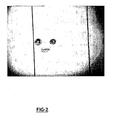
- FIG 1 These aspect defects are illustrated in figure 1 , and are in the form of a visual halo of discoloration whose characteristic dimensions can be in the range of 0.2 mm to 10 cm approximately.
- This visual halo of fading is characteristic of the defects of "smart" active systems of the electrochromic type.
- This discolored area does not represent the actual size of the defect itself, it is only the physical consequence of the presence of the defect.
- This visual defect is concretized by the presence of a leakage current that can be measured.
- the defect or "pinhole” has a real size of the order of 20 to 50 ⁇ m, but its presence in the active system creates phenomena of potential wells around the latter, the effects of which result in discoloration. substantially centered around the latter, over a much larger area that can reach the 2 to 100 mm previously mentioned.
- the laminated substrate is positioned facing a laser.
- the wavelength of the laser beam is adapted so as to be able to pass through without being absorbed the substrate and secondly to be absorbed by the materials forming the layers of the stack of the active system.
- the active system is of the electrochromic type and the wavelength chosen is approximately 1.06 ⁇ m and the laser used is of the pulsed YAG type.
- the fault is then calibrated using a laser-reduced pulse train and the offset between the target and the fault is recorded. When the fault is removed, the measurement of this offset will be incorporated.
- Ablation itself consists of substantially describing a circle around the defect so as to electrically isolate the effective area of the defect and thus minimize the visual impact of this ablation.
- the destruction of the layers forming the stack of the active system takes place by pointing the laser beam at the defect (taking care of the value of the offset), by describing a circle around the latter while pulsing the beam.
- the parameters of the laser beam are as follows (30% of the maximum power, 50 kHz, 0.5 mm radius circle, 80 ⁇ m beam width, 5 m / s beam movement speed).
- the operating conditions of the laser will be adapted.
Landscapes
- Physics & Mathematics (AREA)
- Nonlinear Science (AREA)
- General Physics & Mathematics (AREA)
- Optics & Photonics (AREA)
- Electrochromic Elements, Electrophoresis, Or Variable Reflection Or Absorption Elements (AREA)
- Joining Of Glass To Other Materials (AREA)
- Photovoltaic Devices (AREA)
- Electroluminescent Light Sources (AREA)
- Laser Beam Processing (AREA)
Claims (7)
- Verfahren zur Beseitigung der Defekte innerhalb einer Mehrlagenvorrichtung, die von wenigstens einem ersten Substrat und von wenigstens einem zweiten Substrat gebildet ist, mit Hilfe eines Laserstrahlenbündels, wobei der Mehrlagenaufbau zwischen dem ersten und dem zweiten Substrat wenigstens ein elektrisch steuerbares aktives System einschließt, bestehend in:- einer Phase zum Orten wenigstens eines innerhalb des aktiven Systems befindlichen Defekts,- einer Phase zum Abtragen des Defekts, die darin besteht, letzteren mit Hilfe des Laserstrahls zu umgrenzen, wobei das Abtragen des Defekts in einem elektrischen Isolieren des Umfangsbereichs des Defekts gegenüber dem den Defekt einschließenden aktiven System besteht, wobei der Defekt mit Hilfe einer Vielzahl von Laserimpulsen umgrenzt wird,
dadurch gekennzeichnet, dass eine Phase zum Anpeilen des Defekts mit Hilfe wenigstens eines ersten Laserstrahlimpulses durchgeführt wird, wobei die Anpeilungsphase eine Zwischenphase zur Neueinstellung des Laserstrahls in Abhängigkeit von der zwischen einem der ersten Impulse und dem Defekt festgestellten Abweichung einschließt. - Verfahren nach Anspruch 1, wobei die Phase der Ortung des Defekts auf optischem Weg entweder manuell, menschliches Eingreifen, oder automatisch mit Hilfe einer Bildverarbeitungssoftware durchgeführt wird.
- Verfahren nach Anspruch 1 oder 2, wobei die Anpeilungsphase unter Verwendung einer verminderten Leistung des Laserstrahls durchgeführt wird.
- Verfahren nach einem der vorstehenden Ansprüche, wobei das Abtragen des Defekts in einem Bewegen des Laserstrahls unter Folgen im Wesentlichen des Umfangs des Defekts besteht.
- Verfahren nach einem der vorstehenden Ansprüche, wobei die Wellenlänge des Laserstrahls derart eingestellt ist, dass der Strahl einerseits durch die das aktive System bildenden Lagen aufgenommen wird und andererseits durch das Substrat hindurch geleitet wird.
- Verfahren nach einem der vorstehenden Ansprüche, wobei das Abtragen des Defekts durch das erste Substrat hindurch vollzogen wird.
- Verfahren nach einem der Ansprüche 1 bis 5, wobei das Abtragen des Defekts durch das zweite Substrat hindurch vollzogen wird.
Applications Claiming Priority (3)
| Application Number | Priority Date | Filing Date | Title |
|---|---|---|---|
| FR0212520 | 2002-10-09 | ||
| FR0212520A FR2845684B1 (fr) | 2002-10-09 | 2002-10-09 | Procede de suppression des defauts ponctuels inclus au sein d'un dispositif electrochimique |
| PCT/FR2003/002871 WO2004034138A1 (fr) | 2002-10-09 | 2003-10-01 | Procede de suppression des defauts ponctuels inclus au sein d'un dispositif electrochimique |
Publications (2)
| Publication Number | Publication Date |
|---|---|
| EP1550000A1 EP1550000A1 (de) | 2005-07-06 |
| EP1550000B1 true EP1550000B1 (de) | 2014-06-11 |
Family
ID=32039564
Family Applications (1)
| Application Number | Title | Priority Date | Filing Date |
|---|---|---|---|
| EP03807862.2A Expired - Lifetime EP1550000B1 (de) | 2002-10-09 | 2003-10-01 | Verfahren zur beseitigung von punktuellen defekten bei einer elektrochemischen einrichtung |
Country Status (10)
| Country | Link |
|---|---|
| US (1) | US7531101B2 (de) |
| EP (1) | EP1550000B1 (de) |
| JP (1) | JP2006502545A (de) |
| KR (1) | KR101122635B1 (de) |
| CN (1) | CN100444014C (de) |
| AU (1) | AU2003299440A1 (de) |
| ES (1) | ES2498736T3 (de) |
| FR (1) | FR2845684B1 (de) |
| PL (1) | PL219027B1 (de) |
| WO (1) | WO2004034138A1 (de) |
Families Citing this family (58)
| Publication number | Priority date | Publication date | Assignee | Title |
|---|---|---|---|---|
| US20090189151A1 (en) * | 2006-05-22 | 2009-07-30 | Koninklijke Philips Electronics N.V. | Method for separating a non-emission region from a light emission region within an organic light emitting diode (oled) |
| JP2009064607A (ja) * | 2007-09-05 | 2009-03-26 | Sony Corp | 有機発光表示装置のリペア方法 |
| JP2009266917A (ja) * | 2008-04-23 | 2009-11-12 | Rohm Co Ltd | 有機発光素子および有機発光素子のリペア装置 |
| US9782949B2 (en) | 2008-05-30 | 2017-10-10 | Corning Incorporated | Glass laminated articles and layered articles |
| US8514476B2 (en) | 2008-06-25 | 2013-08-20 | View, Inc. | Multi-pane dynamic window and method for making same |
| KR100932989B1 (ko) | 2008-08-20 | 2009-12-21 | 삼성모바일디스플레이주식회사 | 유기 발광 표시 장치 및 그 제조 방법 |
| US10261381B2 (en) | 2009-03-31 | 2019-04-16 | View, Inc. | Fabrication of low defectivity electrochromic devices |
| US8300298B2 (en) | 2010-04-30 | 2012-10-30 | Soladigm, Inc. | Electrochromic devices |
| US11187954B2 (en) | 2009-03-31 | 2021-11-30 | View, Inc. | Electrochromic cathode materials |
| US12043890B2 (en) | 2009-03-31 | 2024-07-23 | View, Inc. | Electrochromic devices |
| US8764951B2 (en) | 2010-04-30 | 2014-07-01 | View, Inc. | Electrochromic devices |
| US10591795B2 (en) | 2009-03-31 | 2020-03-17 | View, Inc. | Counter electrode for electrochromic devices |
| US9664974B2 (en) | 2009-03-31 | 2017-05-30 | View, Inc. | Fabrication of low defectivity electrochromic devices |
| US10156762B2 (en) | 2009-03-31 | 2018-12-18 | View, Inc. | Counter electrode for electrochromic devices |
| US10852613B2 (en) | 2009-03-31 | 2020-12-01 | View, Inc. | Counter electrode material for electrochromic devices |
| US8582193B2 (en) | 2010-04-30 | 2013-11-12 | View, Inc. | Electrochromic devices |
| US8764950B2 (en) | 2010-04-30 | 2014-07-01 | View, Inc. | Electrochromic devices |
| US9261751B2 (en) | 2010-04-30 | 2016-02-16 | View, Inc. | Electrochromic devices |
| US10303035B2 (en) | 2009-12-22 | 2019-05-28 | View, Inc. | Self-contained EC IGU |
| US12353109B2 (en) | 2009-12-22 | 2025-07-08 | View Operating Corporation | Electrochromic cathode materials |
| US11314139B2 (en) | 2009-12-22 | 2022-04-26 | View, Inc. | Self-contained EC IGU |
| US9759975B2 (en) | 2010-04-30 | 2017-09-12 | View, Inc. | Electrochromic devices |
| US8270059B2 (en) | 2010-08-05 | 2012-09-18 | Soladigm, Inc. | Multi-pane electrochromic windows |
| US9958750B2 (en) | 2010-11-08 | 2018-05-01 | View, Inc. | Electrochromic window fabrication methods |
| US8164818B2 (en) | 2010-11-08 | 2012-04-24 | Soladigm, Inc. | Electrochromic window fabrication methods |
| US10180606B2 (en) | 2010-12-08 | 2019-01-15 | View, Inc. | Connectors for smart windows |
| US8643933B2 (en) | 2011-12-14 | 2014-02-04 | View, Inc. | Connectors for smart windows |
| CN112731720A (zh) | 2010-12-08 | 2021-04-30 | 唯景公司 | 绝缘玻璃装置的改良隔板 |
| US9442339B2 (en) | 2010-12-08 | 2016-09-13 | View, Inc. | Spacers and connectors for insulated glass units |
| US10175549B2 (en) | 2011-03-16 | 2019-01-08 | View, Inc. | Connectors for smart windows |
| US10429712B2 (en) | 2012-04-20 | 2019-10-01 | View, Inc. | Angled bus bar |
| US9454055B2 (en) | 2011-03-16 | 2016-09-27 | View, Inc. | Multipurpose controller for multistate windows |
| US8430707B2 (en) | 2011-05-27 | 2013-04-30 | Sage Electrochromics, Inc. | Apparatus and method for repair of defects in an electronic energy control or display device |
| JP5687339B2 (ja) * | 2011-06-08 | 2015-03-18 | パナソニック株式会社 | 有機el素子及び有機el素子の製造方法 |
| US9885934B2 (en) | 2011-09-14 | 2018-02-06 | View, Inc. | Portable defect mitigators for electrochromic windows |
| HK1200212A1 (en) | 2011-09-14 | 2015-07-31 | View, Inc. | Portable defect mitigator for electrochromic windows |
| US10606142B2 (en) | 2011-12-12 | 2020-03-31 | View, Inc. | Thin-film devices and fabrication |
| CA2859023C (en) | 2011-12-12 | 2023-08-22 | View, Inc. | Thin-film devices and fabrication |
| US12321075B2 (en) | 2011-12-12 | 2025-06-03 | View Operating Corporation | Electrochromic laminates |
| US10739658B2 (en) | 2011-12-12 | 2020-08-11 | View, Inc. | Electrochromic laminates |
| US11048137B2 (en) | 2011-12-12 | 2021-06-29 | View, Inc. | Thin-film devices and fabrication |
| US11719039B2 (en) | 2011-12-14 | 2023-08-08 | View, Inc. | Connectors for smart windows |
| US12153320B2 (en) | 2012-03-13 | 2024-11-26 | View, Inc. | Multi-zone EC windows |
| EP4134733A1 (de) | 2012-03-13 | 2023-02-15 | View, Inc. | Stiftlochabschwächung für optische vorrichtungen |
| US12578609B2 (en) | 2012-03-13 | 2026-03-17 | View Operating Corporation | Methods of controlling multi-zone tintable windows |
| US11635666B2 (en) | 2012-03-13 | 2023-04-25 | View, Inc | Methods of controlling multi-zone tintable windows |
| US9341912B2 (en) | 2012-03-13 | 2016-05-17 | View, Inc. | Multi-zone EC windows |
| WO2013173591A1 (en) * | 2012-05-18 | 2013-11-21 | View, Inc. | Circumscribing defects in optical devices |
| US20230068903A1 (en) * | 2012-05-18 | 2023-03-02 | View, Inc. | Mitigating defects using polygon ablation pattern |
| US11255120B2 (en) | 2012-05-25 | 2022-02-22 | View, Inc. | Tester and electrical connectors for insulated glass units |
| EP2888427B1 (de) | 2012-08-23 | 2021-02-17 | View, Inc. | Photonisch betriebene elektrochrome (ec) vorrichtungen |
| EP3011387A4 (de) | 2013-06-18 | 2016-11-30 | View Inc | Elektrochrome vorrichtungen mit nicht rechteckigen formen |
| US11891327B2 (en) | 2014-05-02 | 2024-02-06 | View, Inc. | Fabrication of low defectivity electrochromic devices |
| US10345671B2 (en) | 2014-09-05 | 2019-07-09 | View, Inc. | Counter electrode for electrochromic devices |
| CN116789175A (zh) | 2014-11-26 | 2023-09-22 | 唯景公司 | 用于电致变色装置的对电极 |
| WO2016100075A1 (en) | 2014-12-15 | 2016-06-23 | View, Inc. | Seals for electrochromic windows |
| WO2018152249A1 (en) | 2017-02-16 | 2018-08-23 | View, Inc. | Solar power dynamic glass for heating and cooling buildings |
| WO2020068813A1 (en) * | 2018-09-26 | 2020-04-02 | Sage Electrochromics, Inc. | Electroactive device and methods |
Family Cites Families (16)
| Publication number | Priority date | Publication date | Assignee | Title |
|---|---|---|---|---|
| JPS62287596A (ja) * | 1986-06-04 | 1987-12-14 | コ−ア株式会社 | エレクトロルミネツセンスパネルの製造方法 |
| JPH02186684A (ja) * | 1989-01-12 | 1990-07-20 | Seiko Epson Corp | 固体記憶膜の形成法 |
| JPH0581878A (ja) * | 1991-09-24 | 1993-04-02 | Nobuyoshi Koshida | 記録された光情報の読み出し方法及び装置 |
| JPH05340905A (ja) * | 1992-06-08 | 1993-12-24 | Idemitsu Kosan Co Ltd | 液晶表示素子の導通点検査方法と導通点修復方法及び導通点検査修復装置 |
| JPH0728099A (ja) * | 1993-07-13 | 1995-01-31 | Nikon Corp | 全固体型エレクトロクロミック素子及びその製造方法 |
| FR2742871B1 (fr) * | 1995-12-22 | 1998-03-13 | Sgs Thomson Microelectronics | Localisation de defauts d'une couche metallique d'un circuit semiconducteur |
| JPH09292635A (ja) * | 1996-04-24 | 1997-11-11 | Fuji Polymertech Kk | エレクトロクロミック素子 |
| FR2753545B1 (fr) * | 1996-09-18 | 1998-10-16 | Saint Gobain Vitrage | Dispositif electrochimique |
| CN1206178A (zh) * | 1997-05-20 | 1999-01-27 | 索尼公司 | 盘基片、盘基片的生产方法和设备 |
| JPH1151875A (ja) * | 1997-08-07 | 1999-02-26 | Hitachi Ltd | 位相欠陥計測装置および位相欠陥計測方法 |
| FR2781084B1 (fr) * | 1998-07-10 | 2007-08-31 | Saint Gobain Vitrage | Procede de traitement d'un dispositif electrochimique |
| JP3840010B2 (ja) * | 1999-10-19 | 2006-11-01 | 東北パイオニア株式会社 | 発光ディスプレイの製造方法 |
| AU2001228239A1 (en) * | 2000-01-27 | 2001-08-07 | National Research Council Of Canada | Method and apparatus for repair of defects in materials with short laser pulses |
| US6518539B2 (en) * | 2000-10-23 | 2003-02-11 | The Regents Of The University Of California | Method for producing damage resistant optics |
| JP2002260857A (ja) * | 2000-12-28 | 2002-09-13 | Semiconductor Energy Lab Co Ltd | 発光装置の作製方法および薄膜形成装置 |
| US6639177B2 (en) * | 2001-03-29 | 2003-10-28 | Gsi Lumonics Corporation | Method and system for processing one or more microstructures of a multi-material device |
-
2002
- 2002-10-09 FR FR0212520A patent/FR2845684B1/fr not_active Expired - Fee Related
-
2003
- 2003-10-01 EP EP03807862.2A patent/EP1550000B1/de not_active Expired - Lifetime
- 2003-10-01 CN CNB2003801012595A patent/CN100444014C/zh not_active Expired - Fee Related
- 2003-10-01 AU AU2003299440A patent/AU2003299440A1/en not_active Abandoned
- 2003-10-01 KR KR1020057005907A patent/KR101122635B1/ko not_active Expired - Fee Related
- 2003-10-01 ES ES03807862.2T patent/ES2498736T3/es not_active Expired - Lifetime
- 2003-10-01 WO PCT/FR2003/002871 patent/WO2004034138A1/fr not_active Ceased
- 2003-10-01 US US10/530,285 patent/US7531101B2/en not_active Expired - Lifetime
- 2003-10-01 JP JP2004542540A patent/JP2006502545A/ja active Pending
- 2003-10-01 PL PL375208A patent/PL219027B1/pl unknown
Also Published As
| Publication number | Publication date |
|---|---|
| US7531101B2 (en) | 2009-05-12 |
| US20070141360A1 (en) | 2007-06-21 |
| AU2003299440A1 (en) | 2004-05-04 |
| WO2004034138A1 (fr) | 2004-04-22 |
| JP2006502545A (ja) | 2006-01-19 |
| EP1550000A1 (de) | 2005-07-06 |
| ES2498736T3 (es) | 2014-09-25 |
| KR20050060091A (ko) | 2005-06-21 |
| KR101122635B1 (ko) | 2012-03-09 |
| PL375208A1 (en) | 2005-11-28 |
| CN100444014C (zh) | 2008-12-17 |
| CN1703653A (zh) | 2005-11-30 |
| FR2845684B1 (fr) | 2006-12-15 |
| PL219027B1 (pl) | 2015-03-31 |
| FR2845684A1 (fr) | 2004-04-16 |
Similar Documents
| Publication | Publication Date | Title |
|---|---|---|
| EP1550000B1 (de) | Verfahren zur beseitigung von punktuellen defekten bei einer elektrochemischen einrichtung | |
| EP2047325B1 (de) | Elektrochemisch/elektrisch steuerbare glasvorrichtung mit veränderlichen optischen und/oder energetischen eigenschaften | |
| EP2307926B1 (de) | Elektrochromes bauelement mit gesteuerter infrarotreflexion | |
| EP1509810B1 (de) | Elektrisch betriebene vorrichtung mit variablen optischen und/oder energetischen eigenschaften | |
| EP1646909B1 (de) | Elektrisch steuerbare einrichtung mit variablen optischen und/oder energieeigenschaften | |
| CA2415479C (fr) | Dispositif electrochimique du type electrochrome ou dispositif photovoltaique et ses moyens de connexion electrique | |
| EP2263118B1 (de) | Elektrochrome vorrichtung mit zahnradeingriff | |
| EP1405135B1 (de) | Elektrisch ansteuerbare elektrochrome vorrichtung mit optisch und/oder energetisch variablen eigenschaften | |
| EP2861421B1 (de) | Glasdach mit leuchtvorrichtung | |
| EP3319794B1 (de) | Fahrzeugverglasung | |
| FR2962818A1 (fr) | Dispositif electrochimique a proprietes de transmission optique et/ou energetique electrocommandables. | |
| FR2791147A1 (fr) | Dispositif electrochimique du type dispositif electrocommandable a proprietes optiques et/ou energetiques variables | |
| WO2005103807A2 (fr) | Procédé d'alimentation d'un dispositif électrocommandable à propriétés optiques et/ou énergétiques variables | |
| FR2904704A1 (fr) | Dispositif electrochimique, et/ou elelctrocommandable du type vitrage et a proprietes optiques et/ou energetiques variables | |
| EP1366387A1 (de) | Elektrisch steuerbare vorrichtung basierend auf optischen und/oder energetischen eigenschaften | |
| WO2007000542A2 (fr) | Electrode de dispositifs electrochimiques/electrocommandables | |
| WO2016192968A1 (fr) | Procédé pour l'alimentation électrique d'un composant électronique d'un vitrage feuilleté, vitrage feuilleté pour la mise en œuvre dudit procédé | |
| FR2977040A1 (fr) | Procede de fabrication d'un dispositif electrochimique a proprietes de transmission optique et/ou energetique electrocommandables |
Legal Events
| Date | Code | Title | Description |
|---|---|---|---|
| PUAI | Public reference made under article 153(3) epc to a published international application that has entered the european phase |
Free format text: ORIGINAL CODE: 0009012 |
|
| 17P | Request for examination filed |
Effective date: 20050307 |
|
| AK | Designated contracting states |
Kind code of ref document: A1 Designated state(s): AT BE BG CH CY CZ DE DK EE ES FI FR GB GR HU IE IT LI LU MC NL PT RO SE SI SK TR |
|
| AX | Request for extension of the european patent |
Extension state: AL LT LV MK |
|
| DAX | Request for extension of the european patent (deleted) | ||
| RIN1 | Information on inventor provided before grant (corrected) |
Inventor name: BETEILLE, FABIEN |
|
| 17Q | First examination report despatched |
Effective date: 20100419 |
|
| RAP1 | Party data changed (applicant data changed or rights of an application transferred) |
Owner name: SAGE ELECTROCHROMICS, INC. |
|
| RIC1 | Information provided on ipc code assigned before grant |
Ipc: B32B 17/10 20060101ALI20131016BHEP Ipc: G02F 1/153 20060101AFI20131016BHEP |
|
| GRAP | Despatch of communication of intention to grant a patent |
Free format text: ORIGINAL CODE: EPIDOSNIGR1 |
|
| INTG | Intention to grant announced |
Effective date: 20140109 |
|
| GRAS | Grant fee paid |
Free format text: ORIGINAL CODE: EPIDOSNIGR3 |
|
| GRAA | (expected) grant |
Free format text: ORIGINAL CODE: 0009210 |
|
| AK | Designated contracting states |
Kind code of ref document: B1 Designated state(s): AT BE BG CH CY CZ DE DK EE ES FI FR GB GR HU IE IT LI LU MC NL PT RO SE SI SK TR |
|
| REG | Reference to a national code |
Ref country code: GB Ref legal event code: FG4D Free format text: NOT ENGLISH |
|
| REG | Reference to a national code |
Ref country code: CH Ref legal event code: EP |
|
| REG | Reference to a national code |
Ref country code: IE Ref legal event code: FG4D Free format text: LANGUAGE OF EP DOCUMENT: FRENCH |
|
| REG | Reference to a national code |
Ref country code: AT Ref legal event code: REF Ref document number: 672522 Country of ref document: AT Kind code of ref document: T Effective date: 20140715 |
|
| REG | Reference to a national code |
Ref country code: DE Ref legal event code: R096 Ref document number: 60346331 Country of ref document: DE Effective date: 20140724 |
|
| REG | Reference to a national code |
Ref country code: CH Ref legal event code: NV Representative=s name: KIRKER AND CIE S.A., CH |
|
| REG | Reference to a national code |
Ref country code: ES Ref legal event code: FG2A Ref document number: 2498736 Country of ref document: ES Kind code of ref document: T3 Effective date: 20140925 |
|
| PG25 | Lapsed in a contracting state [announced via postgrant information from national office to epo] |
Ref country code: GR Free format text: LAPSE BECAUSE OF FAILURE TO SUBMIT A TRANSLATION OF THE DESCRIPTION OR TO PAY THE FEE WITHIN THE PRESCRIBED TIME-LIMIT Effective date: 20140912 Ref country code: FI Free format text: LAPSE BECAUSE OF FAILURE TO SUBMIT A TRANSLATION OF THE DESCRIPTION OR TO PAY THE FEE WITHIN THE PRESCRIBED TIME-LIMIT Effective date: 20140611 |
|
| REG | Reference to a national code |
Ref country code: NL Ref legal event code: VDEP Effective date: 20140611 |
|
| REG | Reference to a national code |
Ref country code: AT Ref legal event code: MK05 Ref document number: 672522 Country of ref document: AT Kind code of ref document: T Effective date: 20140611 |
|
| PG25 | Lapsed in a contracting state [announced via postgrant information from national office to epo] |
Ref country code: SE Free format text: LAPSE BECAUSE OF FAILURE TO SUBMIT A TRANSLATION OF THE DESCRIPTION OR TO PAY THE FEE WITHIN THE PRESCRIBED TIME-LIMIT Effective date: 20140611 |
|
| PG25 | Lapsed in a contracting state [announced via postgrant information from national office to epo] |
Ref country code: PT Free format text: LAPSE BECAUSE OF FAILURE TO SUBMIT A TRANSLATION OF THE DESCRIPTION OR TO PAY THE FEE WITHIN THE PRESCRIBED TIME-LIMIT Effective date: 20141013 Ref country code: RO Free format text: LAPSE BECAUSE OF FAILURE TO SUBMIT A TRANSLATION OF THE DESCRIPTION OR TO PAY THE FEE WITHIN THE PRESCRIBED TIME-LIMIT Effective date: 20140611 Ref country code: SK Free format text: LAPSE BECAUSE OF FAILURE TO SUBMIT A TRANSLATION OF THE DESCRIPTION OR TO PAY THE FEE WITHIN THE PRESCRIBED TIME-LIMIT Effective date: 20140611 Ref country code: EE Free format text: LAPSE BECAUSE OF FAILURE TO SUBMIT A TRANSLATION OF THE DESCRIPTION OR TO PAY THE FEE WITHIN THE PRESCRIBED TIME-LIMIT Effective date: 20140611 |
|
| PGFP | Annual fee paid to national office [announced via postgrant information from national office to epo] |
Ref country code: CZ Payment date: 20140911 Year of fee payment: 12 |
|
| PG25 | Lapsed in a contracting state [announced via postgrant information from national office to epo] |
Ref country code: AT Free format text: LAPSE BECAUSE OF FAILURE TO SUBMIT A TRANSLATION OF THE DESCRIPTION OR TO PAY THE FEE WITHIN THE PRESCRIBED TIME-LIMIT Effective date: 20140611 Ref country code: NL Free format text: LAPSE BECAUSE OF FAILURE TO SUBMIT A TRANSLATION OF THE DESCRIPTION OR TO PAY THE FEE WITHIN THE PRESCRIBED TIME-LIMIT Effective date: 20140611 |
|
| REG | Reference to a national code |
Ref country code: DE Ref legal event code: R097 Ref document number: 60346331 Country of ref document: DE |
|
| PLBE | No opposition filed within time limit |
Free format text: ORIGINAL CODE: 0009261 |
|
| STAA | Information on the status of an ep patent application or granted ep patent |
Free format text: STATUS: NO OPPOSITION FILED WITHIN TIME LIMIT |
|
| PG25 | Lapsed in a contracting state [announced via postgrant information from national office to epo] |
Ref country code: DK Free format text: LAPSE BECAUSE OF FAILURE TO SUBMIT A TRANSLATION OF THE DESCRIPTION OR TO PAY THE FEE WITHIN THE PRESCRIBED TIME-LIMIT Effective date: 20140611 |
|
| 26N | No opposition filed |
Effective date: 20150312 |
|
| PG25 | Lapsed in a contracting state [announced via postgrant information from national office to epo] |
Ref country code: LU Free format text: LAPSE BECAUSE OF FAILURE TO SUBMIT A TRANSLATION OF THE DESCRIPTION OR TO PAY THE FEE WITHIN THE PRESCRIBED TIME-LIMIT Effective date: 20141001 Ref country code: MC Free format text: LAPSE BECAUSE OF FAILURE TO SUBMIT A TRANSLATION OF THE DESCRIPTION OR TO PAY THE FEE WITHIN THE PRESCRIBED TIME-LIMIT Effective date: 20140611 |
|
| REG | Reference to a national code |
Ref country code: DE Ref legal event code: R097 Ref document number: 60346331 Country of ref document: DE Effective date: 20150312 |
|
| REG | Reference to a national code |
Ref country code: IE Ref legal event code: MM4A |
|
| PG25 | Lapsed in a contracting state [announced via postgrant information from national office to epo] |
Ref country code: SI Free format text: LAPSE BECAUSE OF FAILURE TO SUBMIT A TRANSLATION OF THE DESCRIPTION OR TO PAY THE FEE WITHIN THE PRESCRIBED TIME-LIMIT Effective date: 20140611 |
|
| REG | Reference to a national code |
Ref country code: FR Ref legal event code: PLFP Year of fee payment: 13 |
|
| PG25 | Lapsed in a contracting state [announced via postgrant information from national office to epo] |
Ref country code: IE Free format text: LAPSE BECAUSE OF NON-PAYMENT OF DUE FEES Effective date: 20141001 |
|
| PGFP | Annual fee paid to national office [announced via postgrant information from national office to epo] |
Ref country code: ES Payment date: 20150915 Year of fee payment: 13 |
|
| PGFP | Annual fee paid to national office [announced via postgrant information from national office to epo] |
Ref country code: CH Payment date: 20151012 Year of fee payment: 13 Ref country code: IT Payment date: 20151026 Year of fee payment: 13 |
|
| PGFP | Annual fee paid to national office [announced via postgrant information from national office to epo] |
Ref country code: BE Payment date: 20151028 Year of fee payment: 13 |
|
| PG25 | Lapsed in a contracting state [announced via postgrant information from national office to epo] |
Ref country code: CZ Free format text: LAPSE BECAUSE OF NON-PAYMENT OF DUE FEES Effective date: 20151001 |
|
| PG25 | Lapsed in a contracting state [announced via postgrant information from national office to epo] |
Ref country code: BG Free format text: LAPSE BECAUSE OF FAILURE TO SUBMIT A TRANSLATION OF THE DESCRIPTION OR TO PAY THE FEE WITHIN THE PRESCRIBED TIME-LIMIT Effective date: 20140611 |
|
| PG25 | Lapsed in a contracting state [announced via postgrant information from national office to epo] |
Ref country code: CY Free format text: LAPSE BECAUSE OF FAILURE TO SUBMIT A TRANSLATION OF THE DESCRIPTION OR TO PAY THE FEE WITHIN THE PRESCRIBED TIME-LIMIT Effective date: 20140611 |
|
| PG25 | Lapsed in a contracting state [announced via postgrant information from national office to epo] |
Ref country code: HU Free format text: LAPSE BECAUSE OF FAILURE TO SUBMIT A TRANSLATION OF THE DESCRIPTION OR TO PAY THE FEE WITHIN THE PRESCRIBED TIME-LIMIT; INVALID AB INITIO Effective date: 20031001 Ref country code: TR Free format text: LAPSE BECAUSE OF FAILURE TO SUBMIT A TRANSLATION OF THE DESCRIPTION OR TO PAY THE FEE WITHIN THE PRESCRIBED TIME-LIMIT Effective date: 20140611 |
|
| REG | Reference to a national code |
Ref country code: FR Ref legal event code: PLFP Year of fee payment: 14 |
|
| PG25 | Lapsed in a contracting state [announced via postgrant information from national office to epo] |
Ref country code: BE Free format text: LAPSE BECAUSE OF NON-PAYMENT OF DUE FEES Effective date: 20161031 |
|
| REG | Reference to a national code |
Ref country code: CH Ref legal event code: PL |
|
| PG25 | Lapsed in a contracting state [announced via postgrant information from national office to epo] |
Ref country code: CH Free format text: LAPSE BECAUSE OF NON-PAYMENT OF DUE FEES Effective date: 20161031 Ref country code: LI Free format text: LAPSE BECAUSE OF NON-PAYMENT OF DUE FEES Effective date: 20161031 |
|
| REG | Reference to a national code |
Ref country code: FR Ref legal event code: PLFP Year of fee payment: 15 |
|
| PG25 | Lapsed in a contracting state [announced via postgrant information from national office to epo] |
Ref country code: IT Free format text: LAPSE BECAUSE OF NON-PAYMENT OF DUE FEES Effective date: 20161001 |
|
| REG | Reference to a national code |
Ref country code: BE Ref legal event code: MM Effective date: 20161031 |
|
| PG25 | Lapsed in a contracting state [announced via postgrant information from national office to epo] |
Ref country code: ES Free format text: LAPSE BECAUSE OF NON-PAYMENT OF DUE FEES Effective date: 20161002 |
|
| REG | Reference to a national code |
Ref country code: FR Ref legal event code: PLFP Year of fee payment: 16 |
|
| REG | Reference to a national code |
Ref country code: ES Ref legal event code: FD2A Effective date: 20181126 |
|
| PGFP | Annual fee paid to national office [announced via postgrant information from national office to epo] |
Ref country code: GB Payment date: 20220901 Year of fee payment: 20 |
|
| PGFP | Annual fee paid to national office [announced via postgrant information from national office to epo] |
Ref country code: FR Payment date: 20221028 Year of fee payment: 20 |
|
| PGFP | Annual fee paid to national office [announced via postgrant information from national office to epo] |
Ref country code: DE Payment date: 20220621 Year of fee payment: 20 |
|
| REG | Reference to a national code |
Ref country code: DE Ref legal event code: R071 Ref document number: 60346331 Country of ref document: DE |
|
| REG | Reference to a national code |
Ref country code: GB Ref legal event code: PE20 Expiry date: 20230930 |
|
| PG25 | Lapsed in a contracting state [announced via postgrant information from national office to epo] |
Ref country code: GB Free format text: LAPSE BECAUSE OF EXPIRATION OF PROTECTION Effective date: 20230930 |