EP1553627A1 - Matériau de plaque de dissipation thermique sur laquelle est monté un semi-conducteur, et boitier céramique obtenu - Google Patents
Matériau de plaque de dissipation thermique sur laquelle est monté un semi-conducteur, et boitier céramique obtenu Download PDFInfo
- Publication number
- EP1553627A1 EP1553627A1 EP05002607A EP05002607A EP1553627A1 EP 1553627 A1 EP1553627 A1 EP 1553627A1 EP 05002607 A EP05002607 A EP 05002607A EP 05002607 A EP05002607 A EP 05002607A EP 1553627 A1 EP1553627 A1 EP 1553627A1
- Authority
- EP
- European Patent Office
- Prior art keywords
- copper
- composite
- heat dissipation
- dissipation substrate
- semiconductor
- Prior art date
- Legal status (The legal status is an assumption and is not a legal conclusion. Google has not performed a legal analysis and makes no representation as to the accuracy of the status listed.)
- Ceased
Links
Images


Classifications
-
- B—PERFORMING OPERATIONS; TRANSPORTING
- B32—LAYERED PRODUCTS
- B32B—LAYERED PRODUCTS, i.e. PRODUCTS BUILT-UP OF STRATA OF FLAT OR NON-FLAT, e.g. CELLULAR OR HONEYCOMB, FORM
- B32B15/00—Layered products comprising a layer of metal
- B32B15/01—Layered products comprising a layer of metal all layers being exclusively metallic
-
- C—CHEMISTRY; METALLURGY
- C22—METALLURGY; FERROUS OR NON-FERROUS ALLOYS; TREATMENT OF ALLOYS OR NON-FERROUS METALS
- C22C—ALLOYS
- C22C1/00—Making non-ferrous alloys
- C22C1/04—Making non-ferrous alloys by powder metallurgy
- C22C1/0475—Impregnated alloys
-
- C—CHEMISTRY; METALLURGY
- C22—METALLURGY; FERROUS OR NON-FERROUS ALLOYS; TREATMENT OF ALLOYS OR NON-FERROUS METALS
- C22C—ALLOYS
- C22C27/00—Alloys based on rhenium or a refractory metal not mentioned in groups C22C14/00 or C22C16/00
- C22C27/04—Alloys based on tungsten or molybdenum
-
- C—CHEMISTRY; METALLURGY
- C22—METALLURGY; FERROUS OR NON-FERROUS ALLOYS; TREATMENT OF ALLOYS OR NON-FERROUS METALS
- C22F—CHANGING THE PHYSICAL STRUCTURE OF NON-FERROUS METALS AND NON-FERROUS ALLOYS
- C22F1/00—Changing the physical structure of non-ferrous metals or alloys by heat treatment or by hot or cold working
- C22F1/08—Changing the physical structure of non-ferrous metals or alloys by heat treatment or by hot or cold working of copper or alloys based thereon
-
- H—ELECTRICITY
- H10—SEMICONDUCTOR DEVICES; ELECTRIC SOLID-STATE DEVICES NOT OTHERWISE PROVIDED FOR
- H10W—GENERIC PACKAGES, INTERCONNECTIONS, CONNECTORS OR OTHER CONSTRUCTIONAL DETAILS OF DEVICES COVERED BY CLASS H10
- H10W40/00—Arrangements for thermal protection or thermal control
- H10W40/20—Arrangements for cooling
- H10W40/25—Arrangements for cooling characterised by their materials
- H10W40/258—Metallic materials
-
- H—ELECTRICITY
- H10—SEMICONDUCTOR DEVICES; ELECTRIC SOLID-STATE DEVICES NOT OTHERWISE PROVIDED FOR
- H10W—GENERIC PACKAGES, INTERCONNECTIONS, CONNECTORS OR OTHER CONSTRUCTIONAL DETAILS OF DEVICES COVERED BY CLASS H10
- H10W70/00—Package substrates; Interposers; Redistribution layers [RDL]
- H10W70/01—Manufacture or treatment
- H10W70/02—Manufacture or treatment of conductive package substrates serving as an interconnection, e.g. of metal plates
- H10W70/027—Mechanical treatments, e.g. deforming, punching or cutting
-
- B—PERFORMING OPERATIONS; TRANSPORTING
- B22—CASTING; POWDER METALLURGY
- B22F—WORKING METALLIC POWDER; MANUFACTURE OF ARTICLES FROM METALLIC POWDER; MAKING METALLIC POWDER; APPARATUS OR DEVICES SPECIALLY ADAPTED FOR METALLIC POWDER
- B22F2998/00—Supplementary information concerning processes or compositions relating to powder metallurgy
- B22F2998/10—Processes characterised by the sequence of their steps
-
- B—PERFORMING OPERATIONS; TRANSPORTING
- B22—CASTING; POWDER METALLURGY
- B22F—WORKING METALLIC POWDER; MANUFACTURE OF ARTICLES FROM METALLIC POWDER; MAKING METALLIC POWDER; APPARATUS OR DEVICES SPECIALLY ADAPTED FOR METALLIC POWDER
- B22F2999/00—Aspects linked to processes or compositions used in powder metallurgy
-
- H—ELECTRICITY
- H10—SEMICONDUCTOR DEVICES; ELECTRIC SOLID-STATE DEVICES NOT OTHERWISE PROVIDED FOR
- H10W—GENERIC PACKAGES, INTERCONNECTIONS, CONNECTORS OR OTHER CONSTRUCTIONAL DETAILS OF DEVICES COVERED BY CLASS H10
- H10W72/00—Interconnections or connectors in packages
- H10W72/851—Dispositions of multiple connectors or interconnections
- H10W72/874—On different surfaces
- H10W72/884—Die-attach connectors and bond wires
-
- H—ELECTRICITY
- H10—SEMICONDUCTOR DEVICES; ELECTRIC SOLID-STATE DEVICES NOT OTHERWISE PROVIDED FOR
- H10W—GENERIC PACKAGES, INTERCONNECTIONS, CONNECTORS OR OTHER CONSTRUCTIONAL DETAILS OF DEVICES COVERED BY CLASS H10
- H10W76/00—Containers; Fillings or auxiliary members therefor; Seals
- H10W76/10—Containers or parts thereof
- H10W76/12—Containers or parts thereof characterised by their shape
- H10W76/13—Containers comprising a conductive base serving as an interconnection
- H10W76/134—Containers comprising a conductive base serving as an interconnection having other interconnections parallel to the conductive base
-
- H—ELECTRICITY
- H10—SEMICONDUCTOR DEVICES; ELECTRIC SOLID-STATE DEVICES NOT OTHERWISE PROVIDED FOR
- H10W—GENERIC PACKAGES, INTERCONNECTIONS, CONNECTORS OR OTHER CONSTRUCTIONAL DETAILS OF DEVICES COVERED BY CLASS H10
- H10W90/00—Package configurations
- H10W90/701—Package configurations characterised by the relative positions of pads or connectors relative to package parts
- H10W90/751—Package configurations characterised by the relative positions of pads or connectors relative to package parts of bond wires
- H10W90/756—Package configurations characterised by the relative positions of pads or connectors relative to package parts of bond wires between a chip and a stacked lead frame, conducting package substrate or heat sink
Definitions
- This invention relates to a material for use in a heat dissipation substrate for a semiconductor in the fields of IC, microwaves, and optics and, in particular, to a heat dissipation substrate for mounting a semiconductor device, a ceramic package comprising a heat dissipation substrate made of a material for a semiconductor-mounting heat dissipation substrate.
- a heat dissipation member for use in applications of the type is required to have an excellent heat conductivity and to have a coefficient of thermal expansion approximate to that of alumina (Al 2 O 3 ), beryllia (BeO), or aluminum nitride (AIN) which is a main constituent material of the semiconductor or the package.
- alumina Al 2 O 3
- BeO beryllia
- AIN aluminum nitride
- the semiconductor is operated at a higher frequency and increased in capacity. This brings about a situation where the copper- tungsten composite alloy limited in heat conductivity is insufficient.
- the package is assembled by bonding alumina and a heat dissipation substrate by a silver brazing alloy.
- the coefficient of thermal expansion of the composite alloy has a value approximate to that of alumina in a temperature range between normal temperature and about 780 °C at which the silver brazing alloy is solidified, the ratio of copper in the copper-tungsten composite must be suppressed between 10 and 13%. Therefore, limitation is imposed upon the thermal conductivity.
- the thermal conductivity of the composite is determined by its composition. If any defect such as a void is not present in the material and if constituent metals do not make a solid solution so that no alloy is produced, the thermal conductivity is determined by the ratio of the constituent metals. However, if a metal making a solid solution with the constituent metals is added, the thermal conductivity is decreased.
- an iron-group metal such as nickel (Ni) is generally added.
- Ni nickel
- the addition of the iron-group metal is applied in order to improve the wettability and to facilitate infiltration of copper into a void or gap in the porous tungsten material.
- the thermal conductivity is decreased as compared with the binary composite of copper and tungsten.
- the present inventors have al ready proposed a composite which is obtained by press-molding molybdenum powder to produce a powder compact and impregnating the powder compact with copper and which is excellent in thermal conductivity and suitable as a heat dissipation substrate for a semiconductor used in a large-capacity inverter or the like (see Japanese Patent Application No. 9-226361, hereinafter called a prior art 1).
- the composite obtained by the prior art 1 is good in rollability. It has also been proposed that a heat dissipation substrate of a greater size is obtained by a rolling process.
- a large-capacity semiconductor device accompanied with generation of a large amount of heat is used in an increased number of applications.
- One example is an inverter of an automobile energized by electricity as a driving force. In this case, it is necessary to convert electric power of several tens watts.
- a semiconductor device having a rectifying function When a semiconductor device having a rectifying function is driven, a large amount of heat is generated.
- a rectifying device is mounted on an insulator substrate (such as AIN).
- insulator substrate such as AIN.
- a plurality of similar insulator substrates are fixed and attached to a large-sized heat dissipation substrate by soldering.
- the heat dissipation substrate is fixed to the radiator by screws or the like.
- the heat dissipation substrate is required to have an excellent heat conductivity and to have a heat expansion characteristic such that deformation resulting tram a difference in coefficient of thermal expansion during cooling after soldering of the insulator substrates is suppressed small.
- the heat dissipation substrate is required to have a sufficient strength to allow the substrate to be fixed to the radiator by the screws or the like.
- the present inventors have proposed a composite material of molybdenum and copper, which is manufactured without taking into account a rolling rate.
- the light weight can be achieved by reducing the thickness of the heat dissipation substrate.
- the thickness of the heat dissipation substrate is reduced, the heat capacity is decreased.
- the deformation resulting from thermal strain due to the difference in coefficient of thermal expansion in case where the insulator substrates are soldered is increased as compared with the case where the thickness is great.
- the deformation is a hindrance to the contact between the substrate and the radiator and prevents transfer of the heat.
- AIN excellent in thermal conduction is generally used as the insulator substrate to be soldered to the heat dissipate substrate.
- problems such as deformation of the heat dissipation substrate and fracture of the insulator substrate, as a result of the thermal strain.
- the material of the heat dissipation substrate is required to have a coefficient of thermal expansion of 9.0 x 10 -6 /K or less at a temperature of not higher than 400 °C.
- a ceramic package is used to mount a semiconductor device for producing microwaves in the field of communication or the like.
- a heat dissipation substrate having following characteristics in addition to excellent thermal conduction is required in order to release heat produced by the semiconductor device to the outside of the package.
- the ceramic for the ceramic package use is generally made of a material containing Al 2 O 3 as a main component.
- a material containing Al 2 O 3 As the ceramic for the ceramic package, use is generally made of a material containing Al 2 O 3 as a main component.
- the heat dissipation substrate it is required to use a material such that, in case where the substrate is bonded to the ceramic by a high-temperature (about 800 °C) brazing material (CuAg eutictic brazing material or the like), the ceramic is not broken and the heat dissipation substrate is less deformed during cooling after brazing due to the thermal strain resulting from the difference in coefficient of thermal expansion from the ceramic.
- the semiconductor device such as GaAs
- the semiconductor device such as GaAs
- the semiconductor device which produces high-temperature heat during operation and which is poor in thermal conduction
- the Cu-W composite material generally used and the Mo-Cu composite material according to the prior art 1 may be insufficient in thermal conduction.
- CMC [Cu/Mo/Cu] clad material
- the CMC clad material In the CMC clad material, a Cu layer as each surface layer is softened around a brazing temperature (800 °C) and is easily deformed during cooling.
- the clad material exhibits a thermal behavior similar to that of Mo. Therefore, as compared with the ceramic (generally containing Al 2 O 3 as a main component) to be bonded, heat shrinkage is small so that the CMC composite is deformed.
- the deformation prevents sufficient contact with the cooling device. Thus, there is a problem in cooling of the semiconductor.
- Mo as an intermediate layer of the CMC clad material is brittle. Therefore, it a substrate part is punched out by a press from a plate material, cracks tend to occur in the Mo layer.
- the above-mentioned clad material has the soft Cu layers on both sides thereof. Therefore, it is difficult to prevent occurrence of the cracks in the Mo layer during punching
- the substrate part must be produced by electric spark machining which generally requires high machining cast.
- Cu-W and Cu-Mo generally used as the heat dissipation substrate for the semiconductor ceramic package are typically bonded by the silver brazing alloy. Since W and Mo are poor in wettability with the silver brazing material, the surface of the Cu-W or Cu-Mo substrate is subjected to Ni plating. Thus, brazing with the ceramic subjected to metallization requires a Ni plating process for the substrate. In addition, various problems, such as blister, stain, and discoloration, will be caused due to insufficient contact of a Ni plating layer. reliability. Thus, there is a problem in yield or reliability.
- a [Cu/Mo-Cu-composite/Cu] clad material which comprises a Mo-Cu composite decreased in coefficient of thermal expansion by increasing a working rate upon rolling and Cu layers affixed to both surfaces thereof and which has a thermal expansion characteristic such that various problems due to thermal strain do not occur even if it is brazed to ceramic.
- a material for a semiconductor-mounting heat dissipation substrate the material being a copper-molybdenum rolled composite obtained by infiltrating and filing (hereinafter may be referred to as impregnating) melted copper in a void or gap between powder particles of a molybdenum powder compact.
- impregnating melted copper in a void or gap between powder particles of a molybdenum powder compact.
- a material for a semiconductor-mounting heat dissipation substrate of a copper-clad type comprising a copper/copper-molybdenum composite/copper clad material formed by press-bonding copper plates to both surfaces of a rolled composite, the rolled composite containing, by weight, 70 to 60 % molybdenum and 30 to 40 % copper, said rolled composite being formed by impregnating copper into a void between powder particle of molybdenum powder compact, and thereafter primary and secondary rolling in a first and secondary rolling directions once or repeatedly, said first and second directions intersecting to each other, said rolled composite containing powder particles having a flat shape.
- a ceramic package comprising a heat dissipation substrate made of the above-mentioned material for a semiconductor-mounting heat dissipation substrate of a copper-clad type.
- the impregnating temperature is lower than 1200 °C, Cu has a high viscosity and does not sufficiently infiltrate into the powder compact to leave a void or the like. If the impregnating temperature is higher than 1300 °C, the viscosity of Cu is lowered to cause leakage of Cu which has infiltrated. On the other hand, if the total working rate is lower than 60%, Mo is not sufficiently processed or rolled. This makes it difficult to control the coefficient of linear expansion.
- a ceramic package 11 uses a copper-clad rolled composite plate or a rolled composite plate as a heat dissipation substrate 13.
- a semiconductor chip 15 is fixed and connected via an adhesive 17.
- Ceramic 19 as a main body of the ceramic package 11 has an aperture 21 formed at the center of its bottom. Through the aperture 21, the semiconductor chip 15 is inserted into the ceramic 19. A surface of the ceramic 19 outside the aperture 21 and the heat dissipation substrate 13 are bonded through a silver brazing alloy 23. Thus, the ceramic 19 around the semiconductor chip 15 is covered with the heat dissipation substrate 13.
- the ceramic 19 is provided with pins 25 protruding on the side of the rolled composite plate 13 as terminals to be connected to a substrate which is not illustrated in the figure or a connector mounted on the substrate. These pins 25 and the semiconductor chip are electrically connected through bonding wires 27.
- the ceramic 19 and a ceramic lid 29 covering the ceramic are bonded through a low-melting-point glass to enclose the semiconductor chip 15 within the package.
- a ceramic package 33 has a structure in which the semiconductor chip 15 is bonded onto the rolled composite plate 13 as the heat dissipation substrate via an AuSn solder 35.
- the heat dissipation substrate 13 with the semiconductor chip 15 mounted thereon is bonded to ceramic 27 via the silver brazing alloy 23 to close one end thereof.
- the semiconductor chip 15 is encapsulated in the interior of the ceramic 37.
- the semiconductor chip 15 is electrically connected through the bonding wires 27 to inner ends of the pins 25 penetrating through side surfaces of the ceramic 37.
- the ceramic 37 has the other end sealed by bonding the ceramic lid 29 through the low-melting-point glass 31, in the manner similar to the example illustrated in Fig. 1.
- the present inventors have found out that, like the rolled product comprising the composite according to the prior art mentioned above, a material having an extremely small coefficient of thermal expansion at a high temperature can be obtained if heavy rolling exceeding 60% is performed.
- the rolled product is manufactured in the following manner. Molybdenum powder having an average particle size of 2-4 ⁇ m is press-formed at a temperature of 100-200 MPa to obtain a molybdenum powder compact. Into a void between powder particles of the molybdenum powder compact, melted copper is impregnates in a non-oxidizing atmosphere at 1200-1300 °C to obtain a Cu-Mo composite consisting of 70-60% molybdenum in weight ratio, the balance copper.
- the composite is subjected to primary rolling in one direction at a temperature of 100-300 °C and at a working rate of 50% or more and then to secondary rolling as cold rolling at a working rate of 50% or more in a direction perpendicular in the one direction, thereby obtaining a rolled product with a total working rate of 60% or more.
- the rolled product has a coefficient of linear expansion of 7.2-8.3 x 10 -6 /K at 30-800 °C in the secondary rolling direction.
- the rolled product has an extremely small coefficient of thermal expansion because, following an increase in rolling rate, molybdenum particles in the composite are elongated in the rolling direction to change a microstructure of the composite.
- a molybdenum-copper composite is rolled at an increased working rate so that a coefficient of thermal expansion is 8.3 x 10 -6 /K or less at a temperature not higher than 400 °C.
- the copper layers having a high thermal conductivity are affixed to both surfaces of the molybdenum-copper composite.
- a [copper/molybdenum-copper composite/copper] clad material (hereinafter called CPC) is obtained which has a thermal conductivity superior to that of the molybdenum-copper composite and a coefficient of thermal expansion as a clad material not higher than 9.0 x 10 -6 /K.
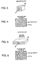
- a composite 39 prior to rolling includes circular-section Mo particles 43 dispersed in a matrix of Cu 41.
- a composite 45 after rolling has a structure in which the Mo particles 43 in the matrix of Cu 41 have a collapsed shape flattened in the rolling direction.
- the Mo particles are gradually flattened in the order of reference numerals 51, 53, 55 and 57 and the coefficient of linear expansion is linearly decreased, as depicted by a straight line 59.
- the composite material of molybdenum and copper which is produced by the method of this invention can be lowered in coefficient of thermal expansion following the increase in working rate upon rolling.
- the CPC produced according to this invention has following characteristics as compares with the CMC.
- the intermediate layer comprises the Mo-Cu composite and contains copper. Therefore, it is possible to lower the temperature upon hot rolling for adhesion of the composite to copper. This brings about energy saving and high adhesion force. Because of little difference in deformability between the cladding material and the intermediate layer, deformation on the layers as a result of rolling is small and the quality is stable.
- the thermal characteristics are superior to those of the CMC because not only heat diffusion is performed in a horizontal (XY) direction but also copper is present in a thickness (Z) direction.
- the coefficient of thermal expansion there is no problem because, by controlling the working rate of the Mo-Cu composite material as the intermediate layer without changing the thickness of the Cu layers, the coefficient of thermal expansion of 8.3 x 10 -6 /K or less, which allows matching with the ceramic, is obtained. Furthermore, Ni platability is more excellent because less exposure of Mo.
- Molybdenum powder having an average particles size of 4 ⁇ m was subjected to hydrostatic press forming at a hydraulic pressure of 150 MPa to form a rectangular plate in dimension of a thickness (T) 12.5 x 180 x 175 mm.
- a copper plate of T 5 x 175 x 175 mm was put on the rectangular plate and heated in a hydrogen atmosphere at 1300 °C so that copper was melted and impregnated into a void in the molybdenum molded product.
- a Cu-Mo composite having a dimension of T 12 x 173 x 168 mm and containing 35 % copper in a weight ration was obtained.
- the composite was heated to 200 °C and repeatedly subjected to primary rolling at a 20% or less reduction until a predetermined thickness was obtained.
- a composite rolled plate of the thickness T 1 x 173 x L mm was formed.
- secondary rolling in a crossing direction was performed at room temperature in a direction perpendicular to the primary rolling direction until T 2 of 1.1 mm is achieved.
- Table 1 Specifically, rolled composite plates having coefficients of linear expansion of 7.0-8.4 x 10 -6 /K at 800 °C were obtained. From these rolled plates A-F, test pieces of 10 x 40 mm were cut out.
- Each test piece was subjected to nickel plating and than hot-brazed at 850 °C to a ceramic frame containing 99.5% or more Al 2 O 3 (after one surface was metallized by tungsten, Ni-plating was performed thereon) by the use of a silver brazing alloy having a silver-copper eutectic composition.
- a silver brazing alloy having a silver-copper eutectic composition.
- the wrap is increased in a convex shape when the coefficient of linear expansion exceeds 8.4 x 10 -6 /K (rolled plate A).
- the coefficient of thermal expansion is smaller than 7.2 x 10 -6 /K or less (rolled plates E, F)
- the wrap is increased in a concave shape. Therefore, the use of the rolled plate A, E or F as a practical substrate caused a defect.
- an impregnated product having a thickness of 18 mm was obtained.
- the impregnated product was rolled by primary rolling of T 1 of 15 mm and finished by secondary rolling to obtain a Cu-Mo composite having T 2 of 3 mm.
- the Cu-Mo composite was sandwiched by Cu plates having T of 1 mm and attached to upper and lower surfaces thereof, and held in an electric furnace in a hydrogen atmosphere heated to 800 °C for 15 minutes.
- the sandwiched composite was made to pass through a roll at a 10% initial reduction (hot rolling) to press-bond Cu and the Cu-Mo composite.
- the CMC Cu/Mo/Cu multilayer material
- press-bonding of Cu and the Cu-Mo composite is more economical and easier.
- the clad material will be called CPC 141.
- the CPC 141 had a coefficient of linear expansion of 8.2 x 10 -6 /K at 400 ⁇ C.
- the rolled plate was processed in the manner similar to example 1 and soldered to a ceramic frame containing AIN to produce a ceramic package like in example 1.
- the wrap was as good as +10 ⁇ m (convex wrap). Any defect such as cracks was not caused in a soldered portion of a ceramic portion.
- the Cu-Mo composite was sandwiched by Cu plates having T of 0.4 mm and attached to upper and lower surfaces thereof and press-bonded by rolling in the manner similar to example 2 to obtain a composite.
- the composite is a CPC clad material of Cu/Cu.-Mo composite/Cu (layer ration being 1 : 4 : 1) having a thickness T of 1.0 mm.
- the CPC 141 had a coefficient of linear expansion of 8.2 x 10 -6 /K at 800 °C.
- the rolled plate was processed in the manner similar to example 1 and Ag brazed to a ceramic frame containing Al 2 O 3 to produce a ceramic package like in example 1.
- the wrap of the Mo-Cu bottom plate was measured. As a result, the wrap was as good as +11 ⁇ m (convex wrap). Any defect such as cracks was not caused in a brazed portion or a ceramic portion.
- the rolled plate was processed in the manner similar to example 1 and Ag brazed to a ceramic frame containing Al 2 O 3 to produce a ceramic package like in example 1.
- the wrap of the Mo-Cu bottom plate was measured. As a result, the wrap was as good a +5 ⁇ m (convex wrap). Any defect such as cracks was caused in a brazed portion or a ceramic portion.
- a semiconductor-mounting heat dissipation substrate which is for use as a heat dissipation substrate of a ceramic package and which is superior in thermal conductivity to a CMC clad material and easy in machining by a punch press and to provide a method of producing the same.
- a semiconductor-mounting heat dissipation substrate of a copper-clad type which has a thermal expansion characteristic such that various problems resulting form thermal strain are not caused even if it is brazed with ceramic and to provide a method of producing the same.
- the semiconductor-mounting heat dissipation substrate according to this invention is most suitable as the heat dissipation substrate of the ceramic package or the like.
Landscapes
- Chemical & Material Sciences (AREA)
- Engineering & Computer Science (AREA)
- Materials Engineering (AREA)
- Mechanical Engineering (AREA)
- Metallurgy (AREA)
- Organic Chemistry (AREA)
- Physics & Mathematics (AREA)
- Thermal Sciences (AREA)
- Crystallography & Structural Chemistry (AREA)
- Cooling Or The Like Of Semiconductors Or Solid State Devices (AREA)
- Powder Metallurgy (AREA)
Applications Claiming Priority (5)
| Application Number | Priority Date | Filing Date | Title |
|---|---|---|---|
| JP2000113006 | 2000-04-14 | ||
| JP2000113006 | 2000-04-14 | ||
| JP2000372405 | 2000-12-07 | ||
| JP2000372405A JP3856640B2 (ja) | 2000-01-26 | 2000-12-07 | 半導体搭載用放熱基板材料、その製造方法、及びそれを用いたセラミックパッケージ |
| EP01919912A EP1231633B1 (fr) | 2000-04-14 | 2001-04-12 | Materiau de plaque de dissipation thermique sur laquelle est monte un semi-conducteur, procede de fabrication et boitier ceramique obtenu |
Related Parent Applications (1)
| Application Number | Title | Priority Date | Filing Date |
|---|---|---|---|
| EP01919912A Division EP1231633B1 (fr) | 2000-04-14 | 2001-04-12 | Materiau de plaque de dissipation thermique sur laquelle est monte un semi-conducteur, procede de fabrication et boitier ceramique obtenu |
Publications (1)
| Publication Number | Publication Date |
|---|---|
| EP1553627A1 true EP1553627A1 (fr) | 2005-07-13 |
Family
ID=26590109
Family Applications (2)
| Application Number | Title | Priority Date | Filing Date |
|---|---|---|---|
| EP05002607A Ceased EP1553627A1 (fr) | 2000-04-14 | 2001-04-12 | Matériau de plaque de dissipation thermique sur laquelle est monté un semi-conducteur, et boitier céramique obtenu |
| EP01919912A Expired - Lifetime EP1231633B1 (fr) | 2000-04-14 | 2001-04-12 | Materiau de plaque de dissipation thermique sur laquelle est monte un semi-conducteur, procede de fabrication et boitier ceramique obtenu |
Family Applications After (1)
| Application Number | Title | Priority Date | Filing Date |
|---|---|---|---|
| EP01919912A Expired - Lifetime EP1231633B1 (fr) | 2000-04-14 | 2001-04-12 | Materiau de plaque de dissipation thermique sur laquelle est monte un semi-conducteur, procede de fabrication et boitier ceramique obtenu |
Country Status (4)
| Country | Link |
|---|---|
| EP (2) | EP1553627A1 (fr) |
| AT (1) | ATE306119T1 (fr) |
| DE (1) | DE60113797T2 (fr) |
| WO (1) | WO2001080313A1 (fr) |
Cited By (5)
| Publication number | Priority date | Publication date | Assignee | Title |
|---|---|---|---|---|
| DE102005046404A1 (de) * | 2005-09-28 | 2007-04-05 | Infineon Technologies Ag | Verfahren zur Minderung von Streuungen in der Durchbiegung von gewalzten Bodenplatten und Halbleitermodul mit einer solchen Bodenplatte |
| CN102489508A (zh) * | 2011-12-06 | 2012-06-13 | 无锡乐普金属科技有限公司 | 钼铜合金箔片的交叉轧制方法 |
| CN102601116A (zh) * | 2012-03-19 | 2012-07-25 | 长沙升华微电子材料有限公司 | 一种铜基电子封装材料的制备方法 |
| CN103143714A (zh) * | 2013-03-29 | 2013-06-12 | 西北有色金属研究院 | 一种Cu/MoCu/Cu三层复合板坯的制备方法 |
| US11646243B2 (en) | 2017-11-18 | 2023-05-09 | Jfe Precision Corporation | Heat sink and method for manufacturing same |
Families Citing this family (5)
| Publication number | Priority date | Publication date | Assignee | Title |
|---|---|---|---|---|
| EP1985718A4 (fr) * | 2006-02-15 | 2009-09-16 | Jfe Prec Corp | ALLIAGE Cr-Cu, SON PROCEDE DE FABRICATION, DISSIPATEUR THERMIQUE POUR SEMICONDUCTEUR ET COMPOSANT DE DISSIPATEUR THERMIQUE POUR SEMICONDUCTEUR |
| US20090035632A1 (en) * | 2007-07-31 | 2009-02-05 | Kirkwood Brad L | Solid oxide fuel cell electrode systems and methods |
| JP5698947B2 (ja) | 2009-10-01 | 2015-04-08 | Jfe精密株式会社 | 電子機器用放熱板およびその製造方法 |
| JP5818045B1 (ja) * | 2014-12-05 | 2015-11-18 | 株式会社半導体熱研究所 | 放熱基板と、それを使用した半導体パッケージと半導体モジュール |
| CN111819684A (zh) * | 2018-03-23 | 2020-10-23 | 三菱综合材料株式会社 | 电子组件安装模块 |
Citations (5)
| Publication number | Priority date | Publication date | Assignee | Title |
|---|---|---|---|---|
| EP0170867A1 (fr) * | 1984-07-21 | 1986-02-12 | Vacuumschmelze GmbH | Procédé de fabrication d'un materiau composite |
| US5493153A (en) * | 1992-11-26 | 1996-02-20 | Tokyo Tungsten Co., Ltd. | Plastic-packaged semiconductor device having a heat sink matched with a plastic package |
| JPH0892667A (ja) * | 1994-09-22 | 1996-04-09 | Tokyo Tungsten Co Ltd | 金属複合材料及びその製造方法 |
| JPH09143649A (ja) * | 1995-11-28 | 1997-06-03 | Tokyo Tungsten Co Ltd | 高放熱性金属複合板材及びそれを用いた高放熱性金属基板 |
| JP2000026926A (ja) * | 1998-07-08 | 2000-01-25 | Tokyo Tungsten Co Ltd | リードフレーム用複合材とそれを用いた半導体パッケージ |
Family Cites Families (2)
| Publication number | Priority date | Publication date | Assignee | Title |
|---|---|---|---|---|
| JP2746279B2 (ja) * | 1990-06-18 | 1998-05-06 | 日本タングステン 株式会社 | 半導体装置用基板材料及びその製造方法 |
| JP3548991B2 (ja) * | 1997-08-22 | 2004-08-04 | 株式会社アライドマテリアル | 放熱基板及びその製造方法 |
-
2001
- 2001-04-12 EP EP05002607A patent/EP1553627A1/fr not_active Ceased
- 2001-04-12 DE DE60113797T patent/DE60113797T2/de not_active Expired - Fee Related
- 2001-04-12 EP EP01919912A patent/EP1231633B1/fr not_active Expired - Lifetime
- 2001-04-12 WO PCT/JP2001/003164 patent/WO2001080313A1/fr not_active Ceased
- 2001-04-12 AT AT01919912T patent/ATE306119T1/de not_active IP Right Cessation
Patent Citations (5)
| Publication number | Priority date | Publication date | Assignee | Title |
|---|---|---|---|---|
| EP0170867A1 (fr) * | 1984-07-21 | 1986-02-12 | Vacuumschmelze GmbH | Procédé de fabrication d'un materiau composite |
| US5493153A (en) * | 1992-11-26 | 1996-02-20 | Tokyo Tungsten Co., Ltd. | Plastic-packaged semiconductor device having a heat sink matched with a plastic package |
| JPH0892667A (ja) * | 1994-09-22 | 1996-04-09 | Tokyo Tungsten Co Ltd | 金属複合材料及びその製造方法 |
| JPH09143649A (ja) * | 1995-11-28 | 1997-06-03 | Tokyo Tungsten Co Ltd | 高放熱性金属複合板材及びそれを用いた高放熱性金属基板 |
| JP2000026926A (ja) * | 1998-07-08 | 2000-01-25 | Tokyo Tungsten Co Ltd | リードフレーム用複合材とそれを用いた半導体パッケージ |
Non-Patent Citations (3)
| Title |
|---|
| PATENT ABSTRACTS OF JAPAN vol. 1996, no. 08 30 August 1996 (1996-08-30) * |
| PATENT ABSTRACTS OF JAPAN vol. 1997, no. 10 31 October 1997 (1997-10-31) * |
| PATENT ABSTRACTS OF JAPAN vol. 2000, no. 04 31 August 2000 (2000-08-31) * |
Cited By (8)
| Publication number | Priority date | Publication date | Assignee | Title |
|---|---|---|---|---|
| DE102005046404A1 (de) * | 2005-09-28 | 2007-04-05 | Infineon Technologies Ag | Verfahren zur Minderung von Streuungen in der Durchbiegung von gewalzten Bodenplatten und Halbleitermodul mit einer solchen Bodenplatte |
| DE102005046404B4 (de) * | 2005-09-28 | 2008-12-24 | Infineon Technologies Ag | Verfahren zur Minderung von Streuungen in der Durchbiegung von gewalzten Bodenplatten und Leistungshalbleitermodul mit einer nach diesem Verfahren hergestellten Bodenplatte |
| US8148198B2 (en) | 2005-09-28 | 2012-04-03 | Infineon Technologies Ag | Method for reducing variations in the bending of rolled base plates and semiconductor module having such a base plate sensor |
| CN102489508A (zh) * | 2011-12-06 | 2012-06-13 | 无锡乐普金属科技有限公司 | 钼铜合金箔片的交叉轧制方法 |
| CN102601116A (zh) * | 2012-03-19 | 2012-07-25 | 长沙升华微电子材料有限公司 | 一种铜基电子封装材料的制备方法 |
| CN103143714A (zh) * | 2013-03-29 | 2013-06-12 | 西北有色金属研究院 | 一种Cu/MoCu/Cu三层复合板坯的制备方法 |
| CN103143714B (zh) * | 2013-03-29 | 2015-01-14 | 西北有色金属研究院 | 一种Cu/MoCu/Cu三层复合板坯的制备方法 |
| US11646243B2 (en) | 2017-11-18 | 2023-05-09 | Jfe Precision Corporation | Heat sink and method for manufacturing same |
Also Published As
| Publication number | Publication date |
|---|---|
| DE60113797D1 (de) | 2006-02-16 |
| DE60113797T2 (de) | 2006-06-08 |
| EP1231633A1 (fr) | 2002-08-14 |
| EP1231633B1 (fr) | 2005-10-05 |
| EP1231633A4 (fr) | 2003-05-28 |
| WO2001080313A1 (fr) | 2001-10-25 |
| ATE306119T1 (de) | 2005-10-15 |
Similar Documents
| Publication | Publication Date | Title |
|---|---|---|
| US20060246314A1 (en) | Method of producing a heat dissipation substrate of molybdenum powder impregnated with copper with rolling in primary and secondary directions | |
| US7083759B2 (en) | Method of producing a heat dissipation substrate of molybdenum powder impregnated with copper with rolling in primary and secondary directions | |
| US5981085A (en) | Composite substrate for heat-generating semiconductor device and semiconductor apparatus using the same | |
| US5972737A (en) | Heat-dissipating package for microcircuit devices and process for manufacture | |
| US5886407A (en) | Heat-dissipating package for microcircuit devices | |
| US4882212A (en) | Electronic packaging of components incorporating a ceramic-glass-metal composite | |
| US6238454B1 (en) | Isotropic carbon/copper composites | |
| EP0788153B1 (fr) | Pièce d'un dispositif semi-conducteur comportant un matériau de substrat de nitrure d'aluminium et méthode de fabrication associée | |
| US5024883A (en) | Electronic packaging of components incorporating a ceramic-glass-metal composite | |
| EP1944116A1 (fr) | Materiau de gaine et son procede de fabrication, procede pour mouler un materiau de gaine et dissipateur thermique utilisant ledit materiau | |
| EP1450401B1 (fr) | Module comprenant une carte de circuit en céramique | |
| US20010038140A1 (en) | High rigidity, multi-layered semiconductor package and method of making the same | |
| US20060263584A1 (en) | Composite material, electrical circuit or electric module | |
| EP1231633B1 (fr) | Materiau de plaque de dissipation thermique sur laquelle est monte un semi-conducteur, procede de fabrication et boitier ceramique obtenu | |
| US6783867B2 (en) | Member for semiconductor device using an aluminum nitride substrate material, and method of manufacturing the same | |
| JP2000323618A (ja) | 銅回路接合基板及びその製造方法 | |
| EP0365275B1 (fr) | Membre refroidisseur d'un matériau composé pour un élément semi-conducteur et procédé pour sa fabrication | |
| US5451817A (en) | Semiconductor-mounting heat-radiative substrates, a method of making and use thereof in semiconductor packages | |
| JPH06268117A (ja) | 半導体装置用放熱基板およびその製造方法 | |
| EP0915512A2 (fr) | Substrat céramique avec un circuit métallique | |
| JP3493833B2 (ja) | 半導体素子搭載用プラスチックパッケージおよびその製造方法 | |
| JP3190282B2 (ja) | 回路基板の製造方法 | |
| GB2327150A (en) | Composite substrate for a heat-generating semiconductor device | |
| JPH04348062A (ja) | 半導体搭載用放熱基板の製造法と該基板を用いた半導体用パッケージ | |
| JP3850312B2 (ja) | 半導体素子収納用パッケージおよび半導体装置 |
Legal Events
| Date | Code | Title | Description |
|---|---|---|---|
| PUAI | Public reference made under article 153(3) epc to a published international application that has entered the european phase |
Free format text: ORIGINAL CODE: 0009012 |
|
| AC | Divisional application: reference to earlier application |
Ref document number: 1231633 Country of ref document: EP Kind code of ref document: P |
|
| AK | Designated contracting states |
Kind code of ref document: A1 Designated state(s): AT DE FR |
|
| 17P | Request for examination filed |
Effective date: 20051219 |
|
| AKX | Designation fees paid |
Designated state(s): AT DE FR |
|
| 17Q | First examination report despatched |
Effective date: 20060123 |
|
| STAA | Information on the status of an ep patent application or granted ep patent |
Free format text: STATUS: THE APPLICATION HAS BEEN REFUSED |
|
| 18R | Application refused |
Effective date: 20090609 |