EP1553812A2 - Halbleiterchip und Schaltungsanordnung mit abgeschirmter Induktivität - Google Patents
Halbleiterchip und Schaltungsanordnung mit abgeschirmter Induktivität Download PDFInfo
- Publication number
- EP1553812A2 EP1553812A2 EP04292385A EP04292385A EP1553812A2 EP 1553812 A2 EP1553812 A2 EP 1553812A2 EP 04292385 A EP04292385 A EP 04292385A EP 04292385 A EP04292385 A EP 04292385A EP 1553812 A2 EP1553812 A2 EP 1553812A2
- Authority
- EP
- European Patent Office
- Prior art keywords
- chip
- inductor
- shielding
- screen
- inductance
- Prior art date
- Legal status (The legal status is an assumption and is not a legal conclusion. Google has not performed a legal analysis and makes no representation as to the accuracy of the status listed.)
- Withdrawn
Links
Images


Classifications
-
- H—ELECTRICITY
- H10—SEMICONDUCTOR DEVICES; ELECTRIC SOLID-STATE DEVICES NOT OTHERWISE PROVIDED FOR
- H10W—GENERIC PACKAGES, INTERCONNECTIONS, CONNECTORS OR OTHER CONSTRUCTIONAL DETAILS OF DEVICES COVERED BY CLASS H10
- H10W20/00—Interconnections in chips, wafers or substrates
- H10W20/40—Interconnections external to wafers or substrates, e.g. back-end-of-line [BEOL] metallisations or vias connecting to gate electrodes
- H10W20/497—Inductive arrangements or effects of, or between, wiring layers
-
- H—ELECTRICITY
- H10—SEMICONDUCTOR DEVICES; ELECTRIC SOLID-STATE DEVICES NOT OTHERWISE PROVIDED FOR
- H10W—GENERIC PACKAGES, INTERCONNECTIONS, CONNECTORS OR OTHER CONSTRUCTIONAL DETAILS OF DEVICES COVERED BY CLASS H10
- H10W42/00—Arrangements for protection of devices
- H10W42/20—Arrangements for protection of devices protecting against electromagnetic or particle radiation, e.g. light, X-rays, gamma-rays or electrons
-
- H—ELECTRICITY
- H10—SEMICONDUCTOR DEVICES; ELECTRIC SOLID-STATE DEVICES NOT OTHERWISE PROVIDED FOR
- H10W—GENERIC PACKAGES, INTERCONNECTIONS, CONNECTORS OR OTHER CONSTRUCTIONAL DETAILS OF DEVICES COVERED BY CLASS H10
- H10W72/00—Interconnections or connectors in packages
- H10W72/071—Connecting or disconnecting
- H10W72/072—Connecting or disconnecting of bump connectors
- H10W72/07251—Connecting or disconnecting of bump connectors characterised by changes in properties of the bump connectors during connecting
-
- H—ELECTRICITY
- H10—SEMICONDUCTOR DEVICES; ELECTRIC SOLID-STATE DEVICES NOT OTHERWISE PROVIDED FOR
- H10W—GENERIC PACKAGES, INTERCONNECTIONS, CONNECTORS OR OTHER CONSTRUCTIONAL DETAILS OF DEVICES COVERED BY CLASS H10
- H10W72/00—Interconnections or connectors in packages
- H10W72/20—Bump connectors, e.g. solder bumps or copper pillars; Dummy bumps; Thermal bumps
-
- H—ELECTRICITY
- H10—SEMICONDUCTOR DEVICES; ELECTRIC SOLID-STATE DEVICES NOT OTHERWISE PROVIDED FOR
- H10W—GENERIC PACKAGES, INTERCONNECTIONS, CONNECTORS OR OTHER CONSTRUCTIONAL DETAILS OF DEVICES COVERED BY CLASS H10
- H10W90/00—Package configurations
- H10W90/701—Package configurations characterised by the relative positions of pads or connectors relative to package parts
-
- H—ELECTRICITY
- H10—SEMICONDUCTOR DEVICES; ELECTRIC SOLID-STATE DEVICES NOT OTHERWISE PROVIDED FOR
- H10W—GENERIC PACKAGES, INTERCONNECTIONS, CONNECTORS OR OTHER CONSTRUCTIONAL DETAILS OF DEVICES COVERED BY CLASS H10
- H10W90/00—Package configurations
- H10W90/701—Package configurations characterised by the relative positions of pads or connectors relative to package parts
- H10W90/721—Package configurations characterised by the relative positions of pads or connectors relative to package parts of bump connectors
- H10W90/724—Package configurations characterised by the relative positions of pads or connectors relative to package parts of bump connectors between a chip and a stacked insulating package substrate, interposer or RDL
Definitions
- the present invention relates to chip circuits, in which the chip has at least one semiconductor substrate and one inductor substantially planar formed on this substrate.
- RF transmission lines which may include oscillator-translators from Voltage Controlled Oscillator (VCO), phase-lock loop (PLL), mixers, preamplifiers, power etc.
- VCO Voltage Controlled Oscillator
- PLL phase-lock loop
- the consequences of this interference phenomenon within a chip are multiple and may include, for example in the case of the VCO, the parasitic line production, modulation of the operating frequency the VCO, the degradation of the phase error or the oscillation of the VCO at a frequency other than that desired.
- US-B-6611041 discloses an integrated circuit comprising a substantially planar inductance and shielding screen parallel to the plane of the inductor and facing the latter, formed within silicon.
- the shape of the screen is intended to prevent any flow of current in the screen and therefore any magnetic field that would be generated.
- This screen is therefore mainly a screen for electrical noise.
- he also makes it possible to optimize the coefficient of quality of the inductance in reducing resistive losses to the substrate. It requires however the integration of an additional element in the substrate and increases the complexity of the chip. In addition, it is not a screen for parasites magnetic.
- screens of shielding located on the outside of an integrated circuit chip, to protect the chip or the integrated circuit of external disturbances.
- These screens are in generally located outside the housing containing the chip and located on the map electronics to shield circuits deemed sensitive and famous circuits disruptors. They are located in particular at a distance from the chip inductors, in order not to modify the magnetic field of the inductors and not to not degrade their quality factor. To do this, these screens are arranged to more than 500 micrometers ( ⁇ m) of inductance.
- US Pat. No. 6,486,534 describes an integrated circuit comprising a first circuit and at least a second circuit in which a Faraday cage comprising vias and a ground plane within the substrate is arranged around the first circuit to protect the second circuit from electromagnetic interference produced by the first circuit (column 2 lines 14-18).
- a sensitive element for example a inductance of a VCO, disturbing elements
- the teaching provided by this document leads to placing one or more Faraday cages around disruptive elements.
- this solution is expensive.
- the sensitive element is not protected from a disturbing element unpredictable external, for example, the finger of a user approaching the VCO.
- the present invention aims at providing a chip circuit comprising at least minus one chip having a shield for the inductance of the chip that is less affected by the limitations of the prior art.
- the invention proposes a chip circuit comprising a chip.
- This chip comprises at least one semiconductor substrate and substantially planar components formed on the substrate. Of these components at least one component emitting electromagnetic radiation and an inductance sensitive to incident electromagnetic radiation, that we want to protect from this radiation.
- the chip circuit comprises at minus a first shielding screen external to the chip, extending parallel to the plane of the sensitive inductance, arranged opposite said inductance sensitive to a distance of less than 500 ⁇ m. This screen of shielding, thus makes it possible to shield the sensitive inductor vis-à-vis transmitter component (s), while preserving the factor quality of the inductance.
- Such shielding screen is inexpensive and does not require the integration of additional electronic functions in the chip. Moreover, it is not only a shielding screen against electric fields, but also against magnetic fields. It is particularly advantageous in the near field, that is to say adapted to the case of blocks disruptive electronic systems and disturbed electronic blocks separated from distance less than ⁇ / 2 ⁇ , where ⁇ is the wavelength of the field considered electromagnetic, which is generally the case for blocks electronic devices located in the same chip. It also helps to protect the inductance of unplanned disturbing elements, such as a finger of a user.
- the distance between the plane of the inductor and the first screen shield is greater than or equal to 100 microns.
- the distance between the sensitive inductor and the emitter component is greater than 1 mm (millimeter).
- the projection orthogonal of the first shielding screen in terms of inductance to protect fully includes the inductor.
- the projection orthogonal of the first shielding screen on the plane of inductance exceeds at least one edge of the inductor over a distance of 150 microns minimum.
- the chip extends parallel to a first support, the distance from the chip to the first support being determined by the diameter of a first type of "bumps" (solder balls) used to electrically connect the chip to the first support, the first shielding screen being made in the first support.
- a first type of "bumps" soldder balls
- a second shielding screen extends parallel to the plane of the inductor and is arranged opposite the inductor to be protected at a distance between 100 and 500 ⁇ m, the first and second shielding screens located on either side of the inductor.
- the chip circuit further includes a second support parallel to the first support, the first and second supports being located on both sides of the chip.
- the distance from the chip to the second support is determined by the diameter of a second type of "bumps" used for electrically connecting the first support to the second support.
- the second shielding screen is made in the second support.
- the chip circuit further includes a second shielding screen extending parallel to the plane of the inductor and disposed opposite the inductor, the first and second shielding screens are finding on both sides of the inductor.
- the second screen has a shape annular and its orthogonal projection in terms of inductance surrounds this last.
- the distance between the plane of the inductor and the second shielding screen is less than or equal to 30 ⁇ m.
- the orthogonal projection of the second screen of shielding on the plane of the inductor exceeds at least one of the edges of the inductance over a distance of 0.25 mm.
- the second shielding screen is formed on the substrate of the chip.
- the chip comprises a VCO
- the sensitive inductance is an element of the VCO
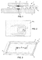
- FIG. 1 shows a chip circuit 1 in a mode of embodiment of the invention.
- the chip circuit 1 comprises at least one chip 2.
- the chip 2 comprises a semiconductor substrate on which various components are formed.
- a VCO comprising a substantially plane inductor 3 formed on the substrate and extending in a plan P1.
- Inductance 3 of the VCO behaves like a receiver antenna sensitive to ambient electromagnetic fields.
- Inductance 3 thus intercepts the lines of fields electromagnetic emissions generated in particular by other integrated the chip that behave vis-à-vis the inductor 3 to be protected as interfering components, introducing parasitic currents and voltages in the inductor 3, and thus in the VCO.
- the chip circuit 1 further comprises a support 4 on which the chip 2 is fixed.
- the support 4 is in the case described here a housing type BGA (from English "Ball Grid Array", which means ball housing) assembled at the chip by soldering balls 5 or "bumps" 5, electrically connecting the chip to the housing BGA 4.
- the chip 2 extends parallel to the BGA box 4 and the distance of the chip to the housing 4 is determined by the diameter of the bumps 5 used.
- the final diameter of the bumps 5 after mounting is 150 ⁇ m.
- the BGA 4 housing includes a screen shield 6.
- This screen of shielding 6 is a metal layer of good electrical conductivity, by example copper, BGA housing 4 (for example the layer 1 of the housing BGA) extending in a plane P2 parallel to the plane P1 of the inductor 3 and arranged in front of the inductor 3.
- the shielding screen 6 for example describes a rectangle in the P2 plan.
- the dimensions of the shielding screen 6 are such that the projection of shielding screen 6 on plane P1 contains fully inductance 3.
- FIG. 2 is shown the orthogonal projection PO6 of the shielding screen 6 on the plane P1 of the inductor 3.
- the shielding screen 6 is connected to the ground of the chip circuit 1.
- the distance z1 between the planes P1 and P2 is less than 500 microns. In a mode of advantageous implementation, z1 is less than 300 microns.
- the shielding screen 6 intercepts, in place of the inductor 3 of the VCO, electromagnetic fields lines radiated from components integrated on the chip 2.
- the chip circuit 1 comprises in in addition to a second support 7, parallel to the housing 4, and which ensures like this last a maintenance function.
- the second support 7 is for example a standard PCB (PCB, "Printed Circuit Board”).
- PCB 7 is attached to the assembly consisting of the housing BGA 4 and the chip 2 with balls soldering or "bumps" 8 arranged between the PCB 7 and the BGA box 4, these bumps 8 electrically connecting these two elements.
- the distance from the chip 2 to the PCB 7 is determined by the diameter of the bumps 8 used.
- the final diameter of the bumps 8 after assembly is 500 microns.
- a second shielding screen 9 is made by a metal layer 7. It is connected to the mass of the chip circuit 1.
- the shielding screen 9 extends in a plane P3 parallel to the plane P1 of inductance 3. It is arranged so that its orthogonal projection on the plane P1 includes inductor 3.
- the distance z2 between the planes P1 and P3 is less than 500 ⁇ m. In an advantageous embodiment, z2 is less than 300 microns.
- the chip circuit 1 comprises a chip 2' which integrates a VCO with a 3 'inductance.
- the orthogonal projections of the screens 6 'and 9' in the plane P1 include the two inductances 3 'and 3 ".
- This attenuation A is represented in FIG. 4a.
- H the attenuation A expressed in decibel (dB)
- H being the field parasitic magnetic undergone by the inductance 3 'before the setting up of the screens 6 'and 9' of the invention
- H ' being the magnetic field undergone by the inductance 3 'after this introduction
- the attenuation A (H) is equal to 20xlog H '/ H.
- the patterned pattern according to the prior art provided only a few attenuation decibels at the parasitic magnetic field.
- the shielding screens considered above were made in a BGA housing and a PCB. Other embodiments may be implemented.
- a first shielding screen can be made on a first support of the chip circuit on which the chip is fixed by welding, by example a support type IPAD ("Integrative Passive and Active Device").
- IPAD Intelligent Passive and Active Device
- a second screen can be realized in this case on a second support circuit to chip, for example a BGA box, the inductor being sandwiched between both screens.
- Such a chip circuit is intended to be fixed on a circuit integrated via solder balls between the BGA housing and the circuit printed.
- the distance between the plane of the inductor and the plans of the screens external to the chip according to the invention is at most 500 ⁇ m, otherwise the shielding is not effective.
- FIG. 4b is shown the attenuation A (H) (as defined above with reference to Figure 4a) depending on the distance Z expressed in micrometer ( ⁇ m) between the plane of the inductance and each of the shield shield planes of a chip circuit similar to that shown in FIG. 3.
- the values given for attenuation correspond to inductance values 3 'and 3 "of 1 nanoHenry (nH), at a distance between the inductances 3 'and 3 "of 1 mm and at a frequency of operation of the 3.6 GHz chip.
- the distance between the plane of the inductor and the plane of each of the screens external to the chip according to the invention is at least 100 microns. If not, the magnetic field generated by the inductor would be disturbed too strongly and the quality factor of the inductance would be degraded too strongly.
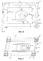
- FIG. 5 is a perspective view of a chip circuit 11 in a second embodiment of the invention.
- This chip circuit includes a chip 12. It further comprises a first shielding screen 13 made to the outside of the chip 12. This is for example the first metal layer of a BGA housing similar to the screen shield 6 shown in Figure 1 and connected to the mass.
- the chip 12 has a substantially plane inductance 14 formed on the layer 5 of the substrate.
- the chip 12 further comprises a shielding screen 15 located in the silicon and formed in metal layer 2 of the substrate of chip 12 and extending parallel to the plane of the inductor 14.
- the shielding screen 15 describes a substantially annular shape, of dimensions such as its projection orthogonal in terms of inductance 14 surrounds it.
- the shielding screen 13 outside the chip 12 and the screen shielding 15 formed in the substrate of the chip 12 are brought into contact electrical through connections 16.
- connections 16 are two in number and each has an electrical connection between the layer 2 and the layer 5 of the chip 12 consisting of a cylinder of vertical metal in silicon, also called via 17.
- Each connection 16 further comprises on the layer 5 of the chip a metal pad or pad ("pad") in English) 18 in contact with the via 17.
- This stud 18 serves as a support base for a metal ball or Bump 19 for electrically connecting the stud 18 to a metal plate 20 located in the plane of the shielding screen 13 and in contact with the latter.
- the dimensions, in the form (XxYxZ) are for example (40 ⁇ m ⁇ 40 ⁇ m ⁇ 6.71 ⁇ m) for via 17, (80 ⁇ m ⁇ 80 ⁇ m ⁇ 2.5 ⁇ m) for pad 18 and (80 ⁇ m ⁇ 80 ⁇ m ⁇ 100 ⁇ m) for the Bump 19.
- FIG. 6 represents a top view of the chip circuit 11 represented in FIG.
- the inductance is centered with respect to the orthogonal projections of two screen shields 13 and 15 in the plane of the inductor 14.
- the shielding screen 13 has a length x1 of 0.75mm and a y1 width of 0.5mm.
- the orthogonal projection of the screen 15 in terms of the inductance in the example considered thus exceeds in length the inductance on both sides 0.25 mm.
- both x11 and y12 are greater than or equal to 0.15 mm.
- the orthogonal projection of the screen 15 in terms of inductance in the example considered thus exceeds width inductance on both sides of 0.25 mm.
- chip circuit 21 having a chip 12 ' is similar to that shown in FIG. Figure 5, except that instead of the two electrical connections 16 between the shield screens 13 and 15, the chip circuit 21 has four connections 16 'between two screens 13' and 15 'similar to the screens 13 and 15.
- Each connection 16 ' comprises a via 17 of dimensions (40 ⁇ m ⁇ 40 ⁇ m ⁇ 6.71 ⁇ m), a pad 18 'of dimension (100 ⁇ m ⁇ 100 ⁇ m ⁇ 2.5 ⁇ m) and a Bump 19 'directly connecting the stud 18' and shielding screen 13.
- the number of connections between a shielding screen in the substrate and a screen shield off the chip, the two screens extending parallel to the plane of the inductor and sandwiching it, allows to adjust the effects of shielding to the parasites achieved.
- the distance between this screen or these screens and the plane of the inductor is between 100 ⁇ m and 300 ⁇ m.
- this screen in silicon will advantageously be at a distance of less than 30 ⁇ m from the plane of inductance. In the case of the silicon technology considered in the description, this distance will be chosen advantageously equal to 2.5 ⁇ m under the inductance.
- this screen in silicon is advantageously will be found at a minimum distance of the inductance of 100 ⁇ m, in the plane defined by the X and Y axes.
- a shield according to the invention of a sensitive inductance desired to protect from disruptive radiation of a component also present on the chip is particularly effective when the distance, in the plane of the inductance between the inductor and the disturbing component is greater or equal to 0.5 mm.
- the invention makes it possible to implement a shielding in the field close to an inductance (i.e. protection is achieved with respect to a disrupter located in the same chip).
- the achieved shielding is effective not only in electric field, but also in magnetic field.
Landscapes
- Semiconductor Integrated Circuits (AREA)
- Shielding Devices Or Components To Electric Or Magnetic Fields (AREA)
- Coils Or Transformers For Communication (AREA)
Applications Claiming Priority (2)
| Application Number | Priority Date | Filing Date | Title |
|---|---|---|---|
| FR0314532 | 2003-12-11 | ||
| FR0314532 | 2003-12-11 |
Publications (2)
| Publication Number | Publication Date |
|---|---|
| EP1553812A2 true EP1553812A2 (de) | 2005-07-13 |
| EP1553812A3 EP1553812A3 (de) | 2013-04-03 |
Family
ID=34586419
Family Applications (1)
| Application Number | Title | Priority Date | Filing Date |
|---|---|---|---|
| EP04292385A Withdrawn EP1553812A3 (de) | 2003-12-11 | 2004-10-07 | Halbleiterchip und Schaltungsanordnung mit abgeschirmter Induktivität |
Country Status (2)
| Country | Link |
|---|---|
| US (1) | US7233055B2 (de) |
| EP (1) | EP1553812A3 (de) |
Families Citing this family (9)
| Publication number | Priority date | Publication date | Assignee | Title |
|---|---|---|---|---|
| US7276420B2 (en) * | 2005-07-11 | 2007-10-02 | Freescale Semiconductor, Inc. | Method of manufacturing a passive integrated matching network for power amplifiers |
| US7999383B2 (en) * | 2006-07-21 | 2011-08-16 | Bae Systems Information And Electronic Systems Integration Inc. | High speed, high density, low power die interconnect system |
| DE102006056777B4 (de) * | 2006-12-01 | 2013-10-10 | Infineon Technologies Ag | Zusammenstellung umfassend ein Trägerelement mit einer Abschirmschicht und einen Chip |
| US8324028B2 (en) * | 2006-12-01 | 2012-12-04 | Infineon Technologies Ag | Assembly comprising a support element and a chip, support element, method for shielding, and method for protecting |
| DE102006057332B4 (de) * | 2006-12-05 | 2018-01-25 | Infineon Technologies Ag | Zusammenbau aufweisend ein Substrat und einen auf dem Substrat montierten Chip |
| JP5103032B2 (ja) * | 2007-03-01 | 2012-12-19 | ルネサスエレクトロニクス株式会社 | 半導体装置 |
| US7892858B2 (en) * | 2008-03-05 | 2011-02-22 | Stats Chippac, Ltd. | Semiconductor package with stacked semiconductor die each having IPD and method of reducing mutual inductive coupling by providing selectable vertical and lateral separation between IPD |
| CN110868793B (zh) * | 2019-11-22 | 2025-08-08 | 中国电子科技集团公司第十三研究所 | 屏蔽结构和三维集成微波电路 |
| US12334430B1 (en) | 2024-04-11 | 2025-06-17 | Globalfoundries U.S. Inc. | Shielded inductor structures and methods of forming the same |
Family Cites Families (13)
| Publication number | Priority date | Publication date | Assignee | Title |
|---|---|---|---|---|
| US6529720B1 (en) * | 1998-12-29 | 2003-03-04 | Koninklijke Philips Electronics N.V. | Integrated circuit of inductive elements |
| US6075700A (en) * | 1999-02-02 | 2000-06-13 | Compaq Computer Corporation | Method and system for controlling radio frequency radiation in microelectronic packages using heat dissipation structures |
| GB2358957B (en) * | 1999-10-27 | 2004-06-23 | Ibm | Ball grid array module |
| JP4776752B2 (ja) | 2000-04-19 | 2011-09-21 | ルネサスエレクトロニクス株式会社 | 半導体装置 |
| US20020140081A1 (en) | 2000-12-07 | 2002-10-03 | Young-Huang Chou | Highly integrated multi-layer circuit module having ceramic substrates with embedded passive devices |
| JP2002198490A (ja) * | 2000-12-26 | 2002-07-12 | Toshiba Corp | 半導体装置 |
| US6534843B2 (en) | 2001-02-10 | 2003-03-18 | International Business Machines Corporation | High Q inductor with faraday shield and dielectric well buried in substrate |
| US6486534B1 (en) * | 2001-02-16 | 2002-11-26 | Ashvattha Semiconductor, Inc. | Integrated circuit die having an interference shield |
| US6850749B2 (en) | 2001-05-30 | 2005-02-01 | Rf Micro Devices, Inc. | Local oscillator architecture to reduce transmitter pulling effect and minimize unwanted sideband |
| JP3792635B2 (ja) * | 2001-12-14 | 2006-07-05 | 富士通株式会社 | 電子装置 |
| US7141883B2 (en) | 2002-10-15 | 2006-11-28 | Silicon Laboratories Inc. | Integrated circuit package configuration incorporating shielded circuit element structure |
| KR20050035904A (ko) | 2003-10-07 | 2005-04-20 | 삼성전기주식회사 | 공통접지 인덕터를 구비한 래더형 벌크탄성파 필터 |
| JP2005353911A (ja) * | 2004-06-11 | 2005-12-22 | Toshiba Corp | 半導体装置 |
-
2004
- 2004-10-07 EP EP04292385A patent/EP1553812A3/de not_active Withdrawn
- 2004-12-10 US US11/009,695 patent/US7233055B2/en not_active Expired - Fee Related
Also Published As
| Publication number | Publication date |
|---|---|
| US20050212084A1 (en) | 2005-09-29 |
| EP1553812A3 (de) | 2013-04-03 |
| US7233055B2 (en) | 2007-06-19 |
Similar Documents
| Publication | Publication Date | Title |
|---|---|---|
| CN101048863B (zh) | 电子部件模块以及无线通信设备 | |
| US8043896B2 (en) | Semiconductor chip, method of manufacturing the semiconductor chip and semiconductor chip package including an inclined via hole | |
| JPH09153839A (ja) | 超高周波帯無線通信装置 | |
| EP1553812A2 (de) | Halbleiterchip und Schaltungsanordnung mit abgeschirmter Induktivität | |
| US7042067B2 (en) | Transmission line with integrated connection pads for circuit elements | |
| EP0942470A2 (de) | Hochfrequenz-Halbleiteranordnung | |
| US7254149B2 (en) | Submount, pedestal, and bond wire assembly for a transistor outline package with reduced bond wire inductance | |
| US20200153071A1 (en) | Integration of self-biased magnetic circulators with microwave devices | |
| US20030180013A1 (en) | Transistor outline package with exteriorly mounted risistors | |
| US6932518B2 (en) | Circuit board having traces with distinct transmission impedances | |
| FR2817399A1 (fr) | Puce electronique multifonctions | |
| US20030178657A1 (en) | Transimpedance amplifier assembly with separate ground leads and separate power leads for included circuits | |
| FR2849538A1 (fr) | Composant discret comprenant des diodes hf en serie et a cathode commune | |
| JP2015184588A (ja) | 光電気集積回路及び光インタポーザ | |
| EP0161166A1 (de) | Kompakter Addierer mit Halbleiteranordnungen im Hyperfrequenz-Betrieb | |
| FR2629271A1 (fr) | Dispositif d'interconnexion et de protection d'une pastille nue de composant hyperfrequence | |
| EP1657749B1 (de) | Mehrlagiges Mikroelektronik-Gehäuse mit interner Abschirmung | |
| FR3096837A1 (fr) | Dispositif électronique comprenant une antenne électromagnétique intégrée | |
| JP2002208595A (ja) | 遮蔽体を備えた電子構成品とその製造方法 | |
| FR3073085B1 (fr) | Ensemble guide d'onde et procede d'assemblage associe | |
| WO2020187821A1 (fr) | Antenne directive compacte, dispositif comportant une telle antenne | |
| US20250149473A1 (en) | Rf absorbing cover integrated in mmic packages | |
| JPH09252191A (ja) | 回路基板装置 | |
| EP3537541B1 (de) | Elektromagnetische entkoppelung | |
| FR2507017A1 (fr) | Microassemblage utilisable en hyperfrequences |
Legal Events
| Date | Code | Title | Description |
|---|---|---|---|
| PUAI | Public reference made under article 153(3) epc to a published international application that has entered the european phase |
Free format text: ORIGINAL CODE: 0009012 |
|
| AK | Designated contracting states |
Kind code of ref document: A2 Designated state(s): AT BE BG CH CY CZ DE DK EE ES FI FR GB GR HU IE IT LI LU MC NL PL PT RO SE SI SK TR |
|
| AX | Request for extension of the european patent |
Extension state: AL HR LT LV MK |
|
| PUAL | Search report despatched |
Free format text: ORIGINAL CODE: 0009013 |
|
| AK | Designated contracting states |
Kind code of ref document: A3 Designated state(s): AT BE BG CH CY CZ DE DK EE ES FI FR GB GR HU IE IT LI LU MC NL PL PT RO SE SI SK TR |
|
| AX | Request for extension of the european patent |
Extension state: AL HR LT LV MK |
|
| RIC1 | Information provided on ipc code assigned before grant |
Ipc: H01L 23/64 20060101ALI20130226BHEP Ipc: H01L 23/552 20060101AFI20130226BHEP Ipc: H01L 27/08 20060101ALI20130226BHEP Ipc: H01L 23/522 20060101ALN20130226BHEP |
|
| AKY | No designation fees paid | ||
| REG | Reference to a national code |
Ref country code: DE Ref legal event code: R108 |
|
| REG | Reference to a national code |
Ref country code: DE Ref legal event code: R108 Effective date: 20131211 |
|
| STAA | Information on the status of an ep patent application or granted ep patent |
Free format text: STATUS: THE APPLICATION IS DEEMED TO BE WITHDRAWN |
|
| 18D | Application deemed to be withdrawn |
Effective date: 20131005 |