EP1554732B1 - Sehr kompakter nichtflüchtiger speicher und ein verfahren dafür - Google Patents
Sehr kompakter nichtflüchtiger speicher und ein verfahren dafür Download PDFInfo
- Publication number
- EP1554732B1 EP1554732B1 EP03754870.8A EP03754870A EP1554732B1 EP 1554732 B1 EP1554732 B1 EP 1554732B1 EP 03754870 A EP03754870 A EP 03754870A EP 1554732 B1 EP1554732 B1 EP 1554732B1
- Authority
- EP
- European Patent Office
- Prior art keywords
- read
- stack
- data
- write
- memory
- Prior art date
- Legal status (The legal status is an assumption and is not a legal conclusion. Google has not performed a legal analysis and makes no representation as to the accuracy of the status listed.)
- Expired - Lifetime
Links
Images


Classifications
-
- G—PHYSICS
- G11—INFORMATION STORAGE
- G11C—STATIC STORES
- G11C7/00—Arrangements for writing information into, or reading information out from, a digital store
- G11C7/06—Sense amplifiers; Associated circuits, e.g. timing or triggering circuits
-
- G—PHYSICS
- G11—INFORMATION STORAGE
- G11C—STATIC STORES
- G11C11/00—Digital stores characterised by the use of particular electric or magnetic storage elements; Storage elements therefor
- G11C11/56—Digital stores characterised by the use of particular electric or magnetic storage elements; Storage elements therefor using storage elements with more than two stable states represented by steps, e.g. of voltage, current, phase, frequency
- G11C11/5621—Digital stores characterised by the use of particular electric or magnetic storage elements; Storage elements therefor using storage elements with more than two stable states represented by steps, e.g. of voltage, current, phase, frequency using charge storage in a floating gate
- G11C11/5628—Programming or writing circuits; Data input circuits
-
- G—PHYSICS
- G11—INFORMATION STORAGE
- G11C—STATIC STORES
- G11C11/00—Digital stores characterised by the use of particular electric or magnetic storage elements; Storage elements therefor
- G11C11/56—Digital stores characterised by the use of particular electric or magnetic storage elements; Storage elements therefor using storage elements with more than two stable states represented by steps, e.g. of voltage, current, phase, frequency
- G11C11/5621—Digital stores characterised by the use of particular electric or magnetic storage elements; Storage elements therefor using storage elements with more than two stable states represented by steps, e.g. of voltage, current, phase, frequency using charge storage in a floating gate
- G11C11/5642—Sensing or reading circuits; Data output circuits
-
- G—PHYSICS
- G11—INFORMATION STORAGE
- G11C—STATIC STORES
- G11C16/00—Erasable programmable read-only memories
- G11C16/02—Erasable programmable read-only memories electrically programmable
- G11C16/04—Erasable programmable read-only memories electrically programmable using variable threshold transistors, e.g. FAMOS
- G11C16/0483—Erasable programmable read-only memories electrically programmable using variable threshold transistors, e.g. FAMOS comprising cells having several storage transistors connected in series
-
- G—PHYSICS
- G11—INFORMATION STORAGE
- G11C—STATIC STORES
- G11C16/00—Erasable programmable read-only memories
- G11C16/02—Erasable programmable read-only memories electrically programmable
- G11C16/06—Auxiliary circuits, e.g. for writing into memory
- G11C16/10—Programming or data input circuits
-
- G—PHYSICS
- G11—INFORMATION STORAGE
- G11C—STATIC STORES
- G11C16/00—Erasable programmable read-only memories
- G11C16/02—Erasable programmable read-only memories electrically programmable
- G11C16/06—Auxiliary circuits, e.g. for writing into memory
- G11C16/24—Bit-line control circuits
-
- G—PHYSICS
- G11—INFORMATION STORAGE
- G11C—STATIC STORES
- G11C16/00—Erasable programmable read-only memories
- G11C16/02—Erasable programmable read-only memories electrically programmable
- G11C16/06—Auxiliary circuits, e.g. for writing into memory
- G11C16/26—Sensing or reading circuits; Data output circuits
-
- G—PHYSICS
- G11—INFORMATION STORAGE
- G11C—STATIC STORES
- G11C5/00—Details of stores covered by group G11C11/00
- G11C5/06—Arrangements for interconnecting storage elements electrically, e.g. by wiring
- G11C5/063—Voltage and signal distribution in integrated semi-conductor memory access lines, e.g. word-line, bit-line, cross-over resistance, propagation delay
-
- G—PHYSICS
- G11—INFORMATION STORAGE
- G11C—STATIC STORES
- G11C7/00—Arrangements for writing information into, or reading information out from, a digital store
- G11C7/10—Input/output [I/O] data interface arrangements, e.g. I/O data control circuits, I/O data buffers
- G11C7/1006—Data managing, e.g. manipulating data before writing or reading out, data bus switches or control circuits therefor
-
- G—PHYSICS
- G11—INFORMATION STORAGE
- G11C—STATIC STORES
- G11C7/00—Arrangements for writing information into, or reading information out from, a digital store
- G11C7/18—Bit line organisation; Bit line lay-out
-
- G—PHYSICS
- G11—INFORMATION STORAGE
- G11C—STATIC STORES
- G11C2216/00—Indexing scheme relating to G11C16/00 and subgroups, for features not directly covered by these groups
- G11C2216/12—Reading and writing aspects of erasable programmable read-only memories
- G11C2216/14—Circuits or methods to write a page or sector of information simultaneously into a nonvolatile memory, typically a complete row or word line in flash memory
Definitions
- This invention relates generally to non-volatile semiconductor memory such as electrically erasable programmable read-only memory (EEPROM) and flash EEPROM, and specifically ones having highly compact and high performance write and read circuits.
- EEPROM electrically erasable programmable read-only memory
- flash EEPROM flash EEPROM
- Solid-state memory capable of nonvolatile storage of charge, particularly in the form of EEPROM and flash EEPROM packaged as a small form factor card, has recently become the storage of choice in a variety of mobile and handheld devices, notably information appliances and consumer electronics products.
- RAM random access memory
- flash memory is non-volatile, retaining its stored data even after power is turned off.
- flash memory is increasingly being used in mass storage applications.
- Conventional mass storage, based on rotating magnetic medium such as hard drives and floppy disks, is unsuitable for the mobile and handheld environment. This is because disk drives tend to be bulky, are prone to mechanical failure and have high latency and high power requirements.
- flash memory both embedded and in the form of a removable card is ideally suited in the mobile and handheld environment because of its small size, low power consumption, high speed and high reliability features.
- the floating gate can hold a range of charges and therefore can be programmed to any threshold voltage level within a threshold voltage window.
- the size of the threshold voltage window is delimited by the minimum and maximum threshold levels of the device, which in turn correspond to the range of the charges that can be programmed onto the floating gate.
- the threshold window generally depends on the memory device's characteristics, operating conditions and history. Each distinct, resolvable threshold voltage level range within the window may, in principle, be used to designate a definite memory state of the cell.
- the memory device may be erased by a number of mechanisms.
- EPROM the memory is bulk erasable by removing the charge from the floating gate by ultraviolet radiation.
- EEPROM a memory cell is electrically erasable, by applying a high voltage to the substrate relative to the control gate so as to induce electrons in the floating gate to tunnel through a thin oxide to the substrate channel region (i.e., Fowler-Nordheim tunneling.)
- the EEPROM is erasable byte by byte.
- flash EEPROM the memory is electrically erasable either all at once or one or more blocks at a time, where a block may consist of 512 bytes or more of memory.
- the memory devices typically comprise one or more memory chips that may be mounted on a card.
- Each memory chip comprises an array of memory cells supported by peripheral circuits such as decoders and erase, write and read circuits.
- peripheral circuits such as decoders and erase, write and read circuits.
- the more sophisticated memory devices also come with a controller that performs intelligent and higher level memory operations and interfacing.
- non-volatile solid-state memory devices may employ different types of memory cells, each type having one or more charge storage element.
- T2 When T2 is turned on by a voltage at the select gate 40, it allows the current in the T1's portion of the channel to pass between the source and drain.
- the select transistor provides a switch along the source-drain channel independent of the voltage at the control gate.
- One advantage is that it can be used to turn off those cells that are still conducting at zero control gate voltage due to their charge depletion (positive) at their floating gates.
- the other advantage is that it allows source side injection programming to be more easily implemented.
- One simple embodiment of the split-channel memory cell is where the select gate and the control gate are connected to the same word line as indicated schematically by a dotted line shown in FIG. 1B .
- This is accomplished by having a charge storage element (floating gate) positioned over one portion of the channel and a control gate structure (which is part of a word line) positioned over the other channel portion as well as over the charge storage element.
- This effectively forms a cell with two transistors in series, one (the memory transistor) with a combination of the amount of charge on the charge storage element and the voltage on the word line controlling the amount of current that can flow through its portion of the channel, and the other (the select transistor) having the word line alone serving as its gate. Examples of such cells, their uses in memory systems and methods of manufacturing them are given in United States patents nos. 5,070,032 , 5,095,344 , 5,315,541 , 5,343,063 , and 5,661,053 .
- a more refined embodiment of the split-channel cell shown in FIG. 1B is when the select gate and the control gate are independent and not connected by the dotted line between them.
- One implementation has the control gates of one column in an array of cells connected to a control (or steering) line perpendicular to the word line. The effect is to relieve the word line from having to perform two functions at the same time when reading or programming a selected cell. Those two functions are (1) to serve as a gate of a select transistor, thus requiring a proper voltage to turn the select transistor on and off, and (2) to drive the voltage of the charge storage element to a desired level through an electric field (capacitive) coupling between the word line and the charge storage element. It is often difficult to perform both of these functions in an optimum manner with a single voltage.
- both the T2 and T1 - right are turned on to allow the current in the T1 - left's portion of the channel to pass between the source and the drain.
- T2 and T1 - left are turned on.
- Erase is effected by having a portion of the select gate polysilicon in close proximity to the floating gate and applying a substantial positive voltage (e.g. 20V) to the select gate so that the electrons stored within the floating gate can tunnel to the select gate polysilicon.
- FIG. 1D illustrates schematically a string of memory cells organized into an NAND cell.
- a pair of select transistors S1, S2 controls the memory transistors chain's connection to the external via the NAND cell's source terminal 54 and drain terminal 56.
- the source select transistor S 1 when the source select transistor S 1 is turned on, the source terminal is coupled to a source line.
- the drain select transistor S2 is turned on, the drain terminal of the NAND cell is coupled to a bit line of the memory array.
- Each memory transistor in the chain has a charge storage element to store a given amount of charge so as to represent an intended memory state.
- a control gate of each memory transistor provides control over read and write operations.
- a control gate of each of the select transistors S1, S2 provides control access to the NAND cell via its source terminal 54 and drain terminal 56 respectively.
- FIG. 1E illustrates schematically a non-volatile memory with a dielectric layer for storing charge.
- a dielectric layer is used.
- Such memory devices utilizing dielectric storage element have been described by Eitan et al., "NROM: A Novel Localized Trapping, 2-Bit Nonvolatile Memory Cell,” IEEE Electron Device Letters, vol. 21, no. 11, November 2000, pp. 543-545 .
- An ONO dielectric layer extends across the channel between source and drain diffusions. The charge for one data bit is localized in the dielectric layer adjacent to the drain, and the charge for the other data bit is localized in the dielectric layer adjacent to the source.
- United States patents nos. 5,768,192 and 6,011,725 disclose a nonvolatile memory cell having a trapping dielectric sandwiched between two silicon dioxide layers. Multi-state data storage is implemented by separately reading the binary states of the spatially separated charge storage regions within the dielectric.
- flash EEPROM devices are implemented with memory cells where each is formed with its control gate and select gate connected together. In this case, there is no need for steering lines and a word line simply connects all the control gates and select gates of cells along each row. Examples of these designs are disclosed in United States patent nos. 5,172,338 and 5,418,752 . In these designs, the word line essentially performed two functions: row selection and supplying control gate voltage to all cells in the row for reading or programming.
- FIG. 3 illustrates an example of an NAND array of memory cells, such as that shown in FIG. 1D .
- a bit line is coupled to the drain terminal 56 of each NAND cell.
- a source line may connect all their source terminals 54.
- the control gates of the NAND cells along a row are connected to a series of corresponding word lines. An entire row of NAND cells can be addressed by turning on the pair of select transistors (see FIG. 1D ) with appropriate voltages on their control gates via the connected word lines.
- the erase unit or block typically stores one or more pages of data, the page being the unit of programming and reading, although more than one page may be programmed or read in a single operation.
- Each page typically stores one or more sectors of data, the size of the sector being defined by the host system.
- An example is a sector of 512 bytes of user data, following a standard established with magnetic disk drives, plus some number of bytes of overhead information about the user data and/or the block in with it is stored.
- At least one current breakpoint level is established so as to partition the conduction window into two regions.
- a cell When a cell is read by applying predetermined, fixed voltages, its source/drain current is resolved into a memory state by comparing with the breakpoint level (or reference current I REF ). If the current read is higher than that of the breakpoint level, the cell is determined to be in one logical state (e.g., a "zero" state). On the other hand, if the current is less than that of the breakpoint level, the cell is determined to be in the other logical state (e.g., a "one" state). Thus, such a two-state cell stores one bit of digital information.
- a reference current source which may be externally programmable, is often provided as part of a memory system to generate the breakpoint level current.
- the conduction window is partitioned into more than two regions by more than one breakpoint such that each cell is capable of storing more than one bit of data.
- the information that a given EEPROM array can store is thus increased with the number of states that each cell can store.
- EEPROM or flash EEPROM with multi-state or multi-level memory cells have been described in U.S. Patent No. 5,172,338 .
- FIG. 4 illustrates the relation between the source-drain current I D and the control gate voltage V CG for four different charges Q1-Q4 that the floating gate may be selectively storing at any one time.
- the four solid I D versus V CG curves represent four possible charge levels that can be programmed on a floating gate of a memory cell, respectively corresponding to four possible memory states.
- the threshold voltage window of a population of cells may range from 0.5V to 3.5V.
- Six memory states may be demarcated by partitioning the threshold window into five regions in interval of 0.5V each.
- FIG. 6A is a schematic block diagram of an individual read/write module 190.
- a sense amplifier determines the current flowing through the drain of an addressed memory transistor connected via a selected bit line. The current depends on the charge stored in the memory transistor and its control gate voltage. For example, in a multi-state EEPROM cell, its floating gate can be charged to one of several different levels. For a 4-level cell, it may be used to store two bits of data. The level detected by the sense amplifier is converted by a level-to-bits conversion logic to a set of data bits to be stored in a data latch.
- the read/write modules forming the read/write circuits 170 can be arranged into various architectures.
- FIG. 6B shows the read/write stack of FIG. 5 implemented conventionally by a stack of read/write modules 190.
- a read/write module may extend over sixteen columns, then a read/write stack 180 with a stack of eight read/write modules can be used to service eight columns in parallel.
- the read/write stack can be coupled via a column decoder to either the eight odd (1, 3, 5, 7, 9,11, 13, 15) columns or the eight even (2, 4, 6, 8, 10, 12, 14, 16) columns among the bank.
- the conventional architecture of interleaving page exacerbates the error caused by neighboring floating gate coupling. Since the even page and the odd page are programmed and read independently of each other, a page may be programmed under one set of condition but read back under an entirely different set of condition, depending on what has happened to the intervening page in the meantime.
- the read errors will become more severe with increasing density, requiring a more accurate read operation and coarser partitioning of the threshold window for multi-state implementation. Performance will suffer and the potential capacity in a multi-state implementation is limited.
- the data to be programmed is inputted into the set of data latches 224 from the data bus 231.
- the program operation under the controller of the state machine comprises a series of programming voltage pulses applied to the control gate of the addressed cell. Each programming pulse is followed by a read back to determine if the cell has been programmed to the desired memory state.
- the processor 222 monitors the read back memory state relative to the desired memory state. When the two are in agreement, the processor 222 sets the bit line latch 214 so as to cause the bit line to be pulled to a state designating program inhibit. This inhibits the cell coupled to the bit line from further programming even if programming pulses appear on its control gate.
- One important feature of the present invention for a block of read/write modules operating in parallel, is the partitioning of each module into a core portion and a common portion, and having the block of core portions operating and sharing with substantially lesser number of common portions.
- This architecture allows duplicative circuits among the individual read/write modules to be factored out, thereby saving space and power. In high density memory chip designs, the saving in space can be as much as fifty percent of the entire read/write circuits for the memory array. This allows the read/write modules to be densely packed so that they can simultaneously serve a contiguous row of memory cells of the memory array.
- FIG. 8A illustrates schematically a compact memory device having a bank of partitioned read/write stacks, according to one embodiment of the present invention.
- the memory device includes a two-dimensional array of memory cells 300, control circuitry 310, and read/write circuits 370.
- the memory array 300 is addressable by word lines via a row decoder 330 and by bit lines via a column decoder 360.
- the read/write circuits 370 is implemented as a bank of partitioned read/write stacks 400 and allows a block of memory cells to be read or programmed in parallel.
- a block multiplexer 350 is provided to multiplex the read/write circuits 370 to the individual blocks.
- communication among a read/write stack 400 is effected by a stack bus and controlled by a stack bus controller 430.
- FIG. 9 illustrates schematically in more detail the read/write circuits shown in FIG. 8A or 8B being organized into a bank of partitioned read/write stacks.
- Each partitioned read/write stack 400 essentially contains a stack of read/write modules servicing a segment of k memory cells in parallel. Each stack is partitioned into a core stack portion 410 and a common stack portion 420. Communication among each read/write stack 400 is effected by an interconnecting stack bus 431 and controlled by the stack bus controller 430.
- Control lines 411 provide control and clock signals from the stack bus controller 430 to each of the core portion of the read/write stacks 410.
- control lines 421 provide control and clock signals from the stack bus controller 430 to each of the common portion of the read/write stacks 420.
- the block is a run of the entire row of cells.
- the block is a subset of cells in the row.
- the subset of cells could be one half of the entire row or one quarter of the entire row.
- the subset of cells could be a run of contiguous cells or one every other cell, or one every predetermined number of cells.
- one problem encountered in high density and high performance memory is the need for reading and programming a block of contiguous row of cells in parallel and the difficulty in accommodating a read/write module for every cell.
- a row of cells is partitioned into two or more interleaving blocks of cells.
- one block of cells consists of cells from even columns and the other block of cells from odd columns.
- the block multiplexer 350 or 350A and 350B will be used to switch the bank of partitioned read/write stacks to either the even or odd block.
- the processor 222 processes the sense amplifier output data together with related state information to obtain a binary read data for the addressed cell.
- the binary data will then be placed on the stack bus 431 and be picked up by the data latches associated with the bit line k.
- the stack bus controller 430 ensures that the binary data derived from the sense amplifier 212-k goes to the data latches associated with it.
- the partitioning and sharing of a common portion 420 by k read/write module cores 210 predicates that a communication channel be established between the partitioned portions. Referring to FIG. 7 , it can be seen that there are at least two connections between the core portion 210 and the common portion 220. Thus, it would seem that at least 2 k connections are needed. These are in addition to the k bit line connections giving a total of 3 k connections to be provided within the k to 2 k columns' width. Thus at the very least, each column must accommodate 1.5 conductive lines. Generally, it is preferably to have a minimum of conductive lines within each column so that the width, and therefore the conductivity, of each line is maximized.
- the implementation of the stack bus 431 allows a reduced number of communication lines for the various portions of the partitioned read/write stack 400.
- a serial bus implementation with only one line is used. In this way for each stack occupying 2 k columns, only one conductive line is required in addition to k existing bit lines, amounting to a total of k +1 conductive lines. This can result in each column having to accommodate approximately 0.5 conductive line, which means that each conductive line can be approximately two-column wide.
- a read/write stack with a serial-bus architecture also allows more freedom of layout so that the placement of the individual portions within the stack (See for example FIG. 11A and 11B ) can be optimized according to a given consideration.
- a set of I/O enabled data latches associated with the block of read/write sense amplifiers are implemented as part of a space efficient shift registers.
- the output signal of the sense amplifier 212 is interpreted by the processor 222 and converted to binary format.
- the converted data amounts to one bit of binary data.
- the converted binary data will be more than one bit. Therefore, for each bit of binary data, there will be a corresponding data latch among a set of data latches.
- the same set of data latches is used as the program data latches.
- the data to be programmed is sent from the host/controller via the data bus to the memory chip and is stored in the same set of data latches.
- the latch is an array in the multi-state case.
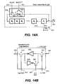
- the data latch stack 224 shown in FIG. 14A may be regarded as a "k+1" compact shift register, comprising k master link modules 510 for holding k bits of data and employing only one slave link module 520 to temporarily buffer data.
- the slave link module 520 is to facilitate shuffling of the items along the chain without losing the stored data in the process.
- This implementation of the latch stack helps reduce the number of latches needed by half as compared to the "2k shift latch" of FIGs. 13A and 13B .
- the k master link modules may share more than one slave link module, but generally with the number of slave modules substantially less than that of the master modules.
- FIG. 14B shows one embodiment of the master or slave link module 510, 520.
- the link module has an input 501 and an output 551.
- the input 501 receives data input from the output of a preceding link module in the chain.
- a transistor 512 controlled by a control signal InCLK, serves as a gate for the input data. When the control signal is HIGH, the data is admitted into the link module. When the control signal is LOW, the data is barred from the module.
- FIG. 15C a copy of D 1 is already saved at S 1 .
- CLK 1 only the master link latch M 1 is turned into an inverter (see FIG. 14C ) and the data D 2 in M 2 is transferred to and latched by M 1 at CLK* 1 .
- D 1 is rotated to S 1 and D 2 is rotated to M 1 as D* 2 .
- CLK 2 only M 2 is turned into an inverter and the data D 3 in M 3 is transferred to and latched by M 2 at CLK* 2 .
- D 3 is now rotated to M 2 .
- CLK 3 and CLK 4 .
Landscapes
- Engineering & Computer Science (AREA)
- Computer Hardware Design (AREA)
- Microelectronics & Electronic Packaging (AREA)
- Read Only Memory (AREA)
- Non-Volatile Memory (AREA)
Claims (15)
- Nichtflüchtige Speichervorrichtung, ein Array von Mehrzustands-Speicherzellen (300) umfassend, die durch eine Vielzahl von Wortleitungen und Bitleitungen adressierbar sind, wobei eine Bank von Lese/Schreib-Schaltungen dazu angeordnet ist, auf einer Gruppe von Speicherzellen parallel über eine assoziierte Gruppe von Bitleitungen zu arbeiten, wobei die Speicherzellen der Gruppe von Speicherzellen durch eine Wortleitung der Vielzahl von Wortleitungen verbunden sind, wobei jede Lese/Schreib-Schaltung in einen Kernteil (210) und einen gemeinsamen Teil (220) partitioniert ist;
dadurch gekennzeichnet, dass:die Bank von Lese/Schreib-Schaltungen (370) in mehrfache Untergruppen von diesen organsiert ist, wobei jede Untergruppe einen Stapel (400) von Lese/Schreib-Schaltungen formt, mehrfache Kernteile (410) von einzelnen Lese/Schreib-Schaltungen der Untergruppe umfassend, wobei jeder der mehrfachen Kernteile (410) an eine Bitleitung der Bitleitungen koppelbar ist für simultanen Lese- oder Programmierzugang durch die mehrfachen Kernteile (410) in einem Stapel;worin jeder Kernteil eine Breite hat, die in einer Richtung senkrecht zu einer Richtung verläuft, in der die Bitleitungen verlaufen, und einen Abtastverstärker (212) umfasst, der dazu angeordnet ist, ein Leitungsstromniveau einer adressierten Speicherzelle abzutasten, worin eine Anzahl von Kernteilen in jeder Untergruppe dieselbe ist wie eine Anzahl von Bitleitungen, an die für gleichzeitigen Lese- oder Programmierzugang anzukoppeln die mehrfachen Kernteile angeordnet sind und über die sich die Breite eines jeden der Kernteile erstreckt;worin jeder Stapel außerdem einen gemeinsamen Teil (420) einschließlich eines Prozessors (222) umfasst, der an jeden der mehrfachen Kernteile (410) der Untergruppe gekoppelt ist und dazu angeordnet ist, mit den mehrfachen Kernteilen der Untergruppe assoziierte Daten zu verarbeiten, und worin die Kernteile und der gemeinsame Teil in der Richtung gestapelt sind, in die sich die Bitleitungen erstrecken; undworin der Prozessor (222) in jedem gemeinsamen Teil angekoppelt ist, um das Leitungsstromniveau zu empfangen, das von den Abtastverstärkern (212) des jeweiligen Stapels abgetastet wird, und dazu angepasst ist, eine Menge von Datenbits vom abgetasteten Leistungsstromniveau zu berechnen;wobei jede Untergruppe einen Bus (431) einschließt, der jeden Kernteil der Untergruppe und den gemeinsamen Teil im Stapel wechselseitig verbindet, wodurch serielle Kommunikation zwischen jedem Kernteil und dem gemeinsamen Teil ermöglicht wird. - Nichtflüchtige Speichervorrichtung nach Anspruch 1, eine Bussteuerung (430) eingeschlossen, die dazu angeordnet ist, Buskommunikation zwischen jedem Kernteil und dem gemeinsamen Teil zu steuern.
- Nichtflüchtige Speichervorrichtung nach einem vorhergehenden Anspruch, worin eine Bitleitung (211) der Bitleitungen, die an einen Kernteil (210) der mehrfachen Kernteile (410) angeschlossen ist, einen Spannungszustand hat, und der Kernteil ein mit der Bitleitung assoziiertes Bitleitungslatch (214) hat, welches Latch dazu angepasst ist, einen Zustand zu latchen, der den Spannungszustand der Bitleitung (211) einstellt.
- Nichtflüchtige Speichervorrichtung nach Anspruch 3, außerdem angeordnet, sodass immer dann, wenn Programmsperrung angefordert wird, das Bitleitungslatch (214) eingestellt wird, um die Bitleitungsspannung zum Sperren der Programmierung einzustellen.
- Nichtflüchtige Speichervorrichtung nach einem vorhergehenden Anspruch, worin jeder gemeinsame Teil einen Satz von Datenlatches (224) zum Speichern der Menge von Datenbits einschließt; und ein Eingabe/Ausgabe-Endgerät (226), an den Satz von Datenlatches gekoppelt, um die Menge von Datenbits auszugeben.
- Nichtflüchtige Speichervorrichtung nach einem vorhergehenden Anspruch, worin jeder gemeinsame Teil einen Satz von Datenlatches (224) zum Speichern der Menge von Datenbits einschließt; und ein Eingabe/Ausgabe-Endgerät (226), an den Satz von Datenlatches (224) gekoppelt, um eine Menge von Datenbits einzugeben, die zu programmieren sind.
- Nichtflüchtige Speichervorrichtung nach Anspruch 6, worin der Prozessor (222) an den Satz von Datenlatches (224) gekoppelt ist, um die Menge von Datenbits zu empfangen, die zu programmieren sind, und dazu angepasst, die Menge von Datenbits, die zu programmieren sind, in ein entsprechendes Leitungsstromniveau der Speicherzelle zu übertragen und das abgetastete Leitungsstromniveau mit dem entsprechenden Leitungsstromniveau zu vergleichen.
- Nichtflüchtige Speichervorrichtung nach einem vorhergehenden Anspruch, so angeordnet, dass ein Segment einer Zeile von Speicherzellen des Arrays von Speicherzellen (300) vom Satz von Lese/Schreib-Schaltungen (370) gleichzeitig gelesen wird.
- Nichtflüchtige Speichervorrichtung nach einem der Ansprüche 1 bis 7, so angeordnet, dass ein Segment einer Zeile von Speicherzellen des Arrays von Speicherzellen (300) durch den Satz von Lese/Schreib-Schaltungen (370) gleichzeitig programmiert wird.
- Nichtflüchtige Speichervorrichtung nach einem der Ansprüche 1 bis 7, worin das Array von Speicherzellen (300) aus Flash-EEPROM-Zellen zusammengesetzt ist.
- Nichtflüchtige Speichervorrichtung nach einem der Ansprüche 1 bis 7, worin das Array von Speicherzellen (300) aus NROM-Zellen zusammengesetzt ist.
- Nichtflüchtige Speichervorrichtung nach Anspruch 8 oder Anspruch 9, worin das Segment eine zusammenhängende Reihe von Speicherzellen über eine ganze Zeile des Arrays (300) ist.
- Nichtflüchtige Speichervorrichtung nach Anspruch 8 oder Anspruch 9, worin das Segment eine zusammenhängende Reihe von Speicherzellen über eine halbe Zeile des Arrays (300) ist.
- Nichtflüchtige Speichervorrichtung nach Anspruch 8 oder Anspruch 9, worin das Segment eine Reihe von jeder zweiten Speicherzelle über eine ganze Zeile des Arrays (300) ist.
- Verfahren zum Formen einer kompakten Gruppe von Lese/Schreib-Schaltungen für eine nichtflüchtige Speichervorrichtung, Folgendes umfassend:Bereitstellen der Bank von Lese/Schreib-Schaltungen zum Betrieb auf einer Gruppe von Mehrzustands-Speicherzellen (300) parallel über eine assoziierte Gruppe von Bitleitungen (211), wobei die Speicherzellen der Gruppe von Speicherzellen durch eine Wortleitung verbunden sind;Partitionieren einer jeden Lese/Schreib-Schaltung in einen Kernteil (210) und einen gemeinsamen Teil (220), worin jeder Kernteil einen Abtastverstärker (212) umfasst, der über eine Bitleitung (211) aus der assoziierten Gruppe von Bitleitungen angekoppelt ist, wobei der Abtastverstärker (212) dazu angeordnet ist, ein Leitungsstromniveau einer adressierten Speicherzelle abzutasten;gekennzeichnet durch:Organisieren der Bank von Lese/Schreib-Schaltungen in mehrfache Untergruppen von diesen, wobei jede Untergruppe einen Stapel von Lese/Schreib-Schaltungen (370) formt mit mehrfachen Kernteilen von einzelnen Lese/Schreib-Schaltungen der Untergruppe, worin jeder Kernteil eine Breite hat, die in einer Richtung senkrecht zu einer Richtung verläuft, in der die Bitleitungen verlaufen, und worin eine Anzahl von Kernteilen in jeder Untergruppe dieselbe ist wie eine Anzahl von Bitleitungen, an die die mehrfachen Kernteile gekoppelt sind und über die sich die Breite eines jeden der Kernteile erstreckt;worin jeder Stapel außerdem einen gemeinsamen Teil umfasst, der an jeden der mehrfachen Kernteile gekoppelt ist, worin die Kernteile und der gemeinsame Teil in der Richtung gestapelt sind, in der die Bitleitungen verlaufen;worin jede Untergruppe einen Bus (431) einschließt, der jeden Kernteil der Untergruppe und den gemeinsamen Teil aus dem Stapel wechselseitig verbindet, wodurch serielle Kommunikation zwischen jedem Kernteil und dem gemeinsamen Teil ermöglicht wird;Bereitstellen eines Prozessors (222) im gemeinsamen Teil (220), um Daten zu verarbeiten, die mit den mehrfachen Kernteilen der Untergruppe assoziiert sind; undworin der Prozessor (222) in jedem gemeinsamen Teil angekoppelt ist, um das Leitungsstromniveau zu empfangen, das von den Abtastverstärkern (212) des jeweiligen Stapels abgetastet wird, und eine Menge von Datenbits vom abgetasteten Leitungsstromniveau berechnet.
Applications Claiming Priority (3)
| Application Number | Priority Date | Filing Date | Title |
|---|---|---|---|
| US254483 | 2002-09-24 | ||
| US10/254,483 US6983428B2 (en) | 2002-09-24 | 2002-09-24 | Highly compact non-volatile memory and method thereof |
| PCT/US2003/030134 WO2004029976A1 (en) | 2002-09-24 | 2003-09-18 | Highly compact non-volatile memory and method thereof |
Publications (3)
| Publication Number | Publication Date |
|---|---|
| EP1554732A1 EP1554732A1 (de) | 2005-07-20 |
| EP1554732B1 true EP1554732B1 (de) | 2015-02-25 |
| EP1554732B8 EP1554732B8 (de) | 2015-04-08 |
Family
ID=31993373
Family Applications (1)
| Application Number | Title | Priority Date | Filing Date |
|---|---|---|---|
| EP03754870.8A Expired - Lifetime EP1554732B8 (de) | 2002-09-24 | 2003-09-18 | Sehr kompakter nichtflüchtiger speicher und ein verfahren dafür |
Country Status (8)
| Country | Link |
|---|---|
| US (6) | US6983428B2 (de) |
| EP (1) | EP1554732B8 (de) |
| JP (1) | JP4814521B2 (de) |
| KR (1) | KR101109651B1 (de) |
| CN (1) | CN1698131B (de) |
| AU (1) | AU2003272673A1 (de) |
| TW (1) | TWI317129B (de) |
| WO (1) | WO2004029976A1 (de) |
Families Citing this family (133)
| Publication number | Priority date | Publication date | Assignee | Title |
|---|---|---|---|---|
| US7170802B2 (en) * | 2003-12-31 | 2007-01-30 | Sandisk Corporation | Flexible and area efficient column redundancy for non-volatile memories |
| US6985388B2 (en) * | 2001-09-17 | 2006-01-10 | Sandisk Corporation | Dynamic column block selection |
| US6891753B2 (en) * | 2002-09-24 | 2005-05-10 | Sandisk Corporation | Highly compact non-volatile memory and method therefor with internal serial buses |
| US7327619B2 (en) * | 2002-09-24 | 2008-02-05 | Sandisk Corporation | Reference sense amplifier for non-volatile memory |
| US7196931B2 (en) * | 2002-09-24 | 2007-03-27 | Sandisk Corporation | Non-volatile memory and method with reduced source line bias errors |
| US7046568B2 (en) | 2002-09-24 | 2006-05-16 | Sandisk Corporation | Memory sensing circuit and method for low voltage operation |
| US6987693B2 (en) * | 2002-09-24 | 2006-01-17 | Sandisk Corporation | Non-volatile memory and method with reduced neighboring field errors |
| US7324393B2 (en) * | 2002-09-24 | 2008-01-29 | Sandisk Corporation | Method for compensated sensing in non-volatile memory |
| US6983428B2 (en) | 2002-09-24 | 2006-01-03 | Sandisk Corporation | Highly compact non-volatile memory and method thereof |
| US7443757B2 (en) | 2002-09-24 | 2008-10-28 | Sandisk Corporation | Non-volatile memory and method with reduced bit line crosstalk errors |
| US7064980B2 (en) * | 2003-09-17 | 2006-06-20 | Sandisk Corporation | Non-volatile memory and method with bit line coupled compensation |
| US6956770B2 (en) | 2003-09-17 | 2005-10-18 | Sandisk Corporation | Non-volatile memory and method with bit line compensation dependent on neighboring operating modes |
| US7257799B2 (en) * | 2003-11-14 | 2007-08-14 | Lsi Corporation | Flexible design for memory use in integrated circuits |
| US7057939B2 (en) | 2004-04-23 | 2006-06-06 | Sandisk Corporation | Non-volatile memory and control with improved partial page program capability |
| US7490283B2 (en) | 2004-05-13 | 2009-02-10 | Sandisk Corporation | Pipelined data relocation and improved chip architectures |
| US7259420B2 (en) * | 2004-07-28 | 2007-08-21 | International Business Machines Corporation | Multiple-gate device with floating back gate |
| US7158421B2 (en) * | 2005-04-01 | 2007-01-02 | Sandisk Corporation | Use of data latches in multi-phase programming of non-volatile memories |
| US7120051B2 (en) * | 2004-12-14 | 2006-10-10 | Sandisk Corporation | Pipelined programming of non-volatile memories using early data |
| US7420847B2 (en) * | 2004-12-14 | 2008-09-02 | Sandisk Corporation | Multi-state memory having data recovery after program fail |
| US7849381B2 (en) * | 2004-12-21 | 2010-12-07 | Sandisk Corporation | Method for copying data in reprogrammable non-volatile memory |
| US20060140007A1 (en) | 2004-12-29 | 2006-06-29 | Raul-Adrian Cernea | Non-volatile memory and method with shared processing for an aggregate of read/write circuits |
| US7447078B2 (en) * | 2005-04-01 | 2008-11-04 | Sandisk Corporation | Method for non-volatile memory with background data latch caching during read operations |
| US7206230B2 (en) | 2005-04-01 | 2007-04-17 | Sandisk Corporation | Use of data latches in cache operations of non-volatile memories |
| US7463521B2 (en) | 2005-04-01 | 2008-12-09 | Sandisk Corporation | Method for non-volatile memory with managed execution of cached data |
| US7187585B2 (en) * | 2005-04-05 | 2007-03-06 | Sandisk Corporation | Read operation for non-volatile storage that includes compensation for coupling |
| US7196946B2 (en) * | 2005-04-05 | 2007-03-27 | Sandisk Corporation | Compensating for coupling in non-volatile storage |
| US7196928B2 (en) * | 2005-04-05 | 2007-03-27 | Sandisk Corporation | Compensating for coupling during read operations of non-volatile memory |
| US7190621B2 (en) * | 2005-06-03 | 2007-03-13 | Infineon Technologies Ag | Sensing scheme for a non-volatile semiconductor memory cell |
| US7259993B2 (en) * | 2005-06-03 | 2007-08-21 | Infineon Technologies Ag | Reference scheme for a non-volatile semiconductor memory device |
| US7218552B1 (en) | 2005-09-09 | 2007-05-15 | Sandisk Corporation | Last-first mode and method for programming of non-volatile memory with reduced program disturb |
| US7170788B1 (en) | 2005-09-09 | 2007-01-30 | Sandisk Corporation | Last-first mode and apparatus for programming of non-volatile memory with reduced program disturb |
| US7366022B2 (en) * | 2005-10-27 | 2008-04-29 | Sandisk Corporation | Apparatus for programming of multi-state non-volatile memory using smart verify |
| US7301817B2 (en) * | 2005-10-27 | 2007-11-27 | Sandisk Corporation | Method for programming of multi-state non-volatile memory using smart verify |
| US7447066B2 (en) * | 2005-11-08 | 2008-11-04 | Sandisk Corporation | Memory with retargetable memory cell redundancy |
| US7262994B2 (en) * | 2005-12-06 | 2007-08-28 | Sandisk Corporation | System for reducing read disturb for non-volatile storage |
| US7349258B2 (en) * | 2005-12-06 | 2008-03-25 | Sandisk Corporation | Reducing read disturb for non-volatile storage |
| US7349260B2 (en) | 2005-12-29 | 2008-03-25 | Sandisk Corporation | Alternate row-based reading and writing for non-volatile memory |
| US7443726B2 (en) * | 2005-12-29 | 2008-10-28 | Sandisk Corporation | Systems for alternate row-based reading and writing for non-volatile memory |
| US7499319B2 (en) * | 2006-03-03 | 2009-03-03 | Sandisk Corporation | Read operation for non-volatile storage with compensation for coupling |
| US7436733B2 (en) * | 2006-03-03 | 2008-10-14 | Sandisk Corporation | System for performing read operation on non-volatile storage with compensation for coupling |
| KR100719382B1 (ko) * | 2006-04-10 | 2007-05-18 | 삼성전자주식회사 | 세 개의 트랜지스터들이 두 개의 셀을 구성하는 비휘발성메모리 소자 |
| JP2007281481A (ja) * | 2006-04-10 | 2007-10-25 | Samsung Electronics Co Ltd | 不揮発性メモリを有する半導体素子及びその形成方法 |
| EP2016590B1 (de) | 2006-05-05 | 2011-10-26 | SanDisk Corporation | Nicht flüchtiger speicher mit hintergrund-datensperren-caching während leseoperationen und entsprechende verfahren |
| TWI427637B (zh) * | 2006-05-05 | 2014-02-21 | Sandisk Technologies Inc | 在程式執行期間具有背景資料鎖存快取的非揮發性記憶體及方法 |
| CN103280239B (zh) * | 2006-05-12 | 2016-04-06 | 苹果公司 | 存储设备中的失真估计和消除 |
| US20070266296A1 (en) * | 2006-05-15 | 2007-11-15 | Conley Kevin M | Nonvolatile Memory with Convolutional Coding |
| US7840875B2 (en) * | 2006-05-15 | 2010-11-23 | Sandisk Corporation | Convolutional coding methods for nonvolatile memory |
| KR100778082B1 (ko) * | 2006-05-18 | 2007-11-21 | 삼성전자주식회사 | 단일의 래치 구조를 갖는 멀티-비트 플래시 메모리 장치,그것의 프로그램 방법, 그리고 그것을 포함하는 메모리카드 |
| US7457163B2 (en) | 2006-06-01 | 2008-11-25 | Sandisk Corporation | System for verifying non-volatile storage using different voltages |
| US7440331B2 (en) | 2006-06-01 | 2008-10-21 | Sandisk Corporation | Verify operation for non-volatile storage using different voltages |
| US7310272B1 (en) * | 2006-06-02 | 2007-12-18 | Sandisk Corporation | System for performing data pattern sensitivity compensation using different voltage |
| US7450421B2 (en) * | 2006-06-02 | 2008-11-11 | Sandisk Corporation | Data pattern sensitivity compensation using different voltage |
| US7606084B2 (en) * | 2006-06-19 | 2009-10-20 | Sandisk Corporation | Programming differently sized margins and sensing with compensations at select states for improved read operations in non-volatile memory |
| US7352628B2 (en) * | 2006-06-19 | 2008-04-01 | Sandisk Corporation | Systems for programming differently sized margins and sensing with compensations at select states for improved read operations in a non-volatile memory |
| US7885119B2 (en) * | 2006-07-20 | 2011-02-08 | Sandisk Corporation | Compensating for coupling during programming |
| US7443729B2 (en) * | 2006-07-20 | 2008-10-28 | Sandisk Corporation | System that compensates for coupling based on sensing a neighbor using coupling |
| US7495953B2 (en) * | 2006-07-20 | 2009-02-24 | Sandisk Corporation | System for configuring compensation |
| US7522454B2 (en) * | 2006-07-20 | 2009-04-21 | Sandisk Corporation | Compensating for coupling based on sensing a neighbor using coupling |
| US7506113B2 (en) * | 2006-07-20 | 2009-03-17 | Sandisk Corporation | Method for configuring compensation |
| US7400535B2 (en) * | 2006-07-20 | 2008-07-15 | Sandisk Corporation | System that compensates for coupling during programming |
| US7518914B2 (en) * | 2006-08-07 | 2009-04-14 | Micron Technology, Inc. | Non-volatile memory device with both single and multiple level cells |
| KR100800378B1 (ko) * | 2006-08-24 | 2008-02-01 | 삼성전자주식회사 | 메모리 소자 및 그의 제조방법 |
| US7885112B2 (en) * | 2007-09-07 | 2011-02-08 | Sandisk Corporation | Nonvolatile memory and method for on-chip pseudo-randomization of data within a page and between pages |
| US7734861B2 (en) * | 2006-09-08 | 2010-06-08 | Sandisk Corporation | Pseudo random and command driven bit compensation for the cycling effects in flash memory |
| US7606966B2 (en) * | 2006-09-08 | 2009-10-20 | Sandisk Corporation | Methods in a pseudo random and command driven bit compensation for the cycling effects in flash memory |
| US7904783B2 (en) * | 2006-09-28 | 2011-03-08 | Sandisk Corporation | Soft-input soft-output decoder for nonvolatile memory |
| US7818653B2 (en) * | 2006-09-28 | 2010-10-19 | Sandisk Corporation | Methods of soft-input soft-output decoding for nonvolatile memory |
| US7805663B2 (en) * | 2006-09-28 | 2010-09-28 | Sandisk Corporation | Methods of adapting operation of nonvolatile memory |
| US20080092015A1 (en) * | 2006-09-28 | 2008-04-17 | Yigal Brandman | Nonvolatile memory with adaptive operation |
| US7684247B2 (en) * | 2006-09-29 | 2010-03-23 | Sandisk Corporation | Reverse reading in non-volatile memory with compensation for coupling |
| US7447076B2 (en) * | 2006-09-29 | 2008-11-04 | Sandisk Corporation | Systems for reverse reading in non-volatile memory with compensation for coupling |
| US7904780B2 (en) * | 2006-11-03 | 2011-03-08 | Sandisk Corporation | Methods of modulating error correction coding |
| US7904788B2 (en) * | 2006-11-03 | 2011-03-08 | Sandisk Corporation | Methods of varying read threshold voltage in nonvolatile memory |
| US7558109B2 (en) * | 2006-11-03 | 2009-07-07 | Sandisk Corporation | Nonvolatile memory with variable read threshold |
| US8001441B2 (en) * | 2006-11-03 | 2011-08-16 | Sandisk Technologies Inc. | Nonvolatile memory with modulated error correction coding |
| US7495962B2 (en) * | 2006-12-29 | 2009-02-24 | Sandisk Corporation | Alternating read mode |
| US7606070B2 (en) * | 2006-12-29 | 2009-10-20 | Sandisk Corporation | Systems for margined neighbor reading for non-volatile memory read operations including coupling compensation |
| US7590002B2 (en) * | 2006-12-29 | 2009-09-15 | Sandisk Corporation | Resistance sensing and compensation for non-volatile storage |
| US7440324B2 (en) * | 2006-12-29 | 2008-10-21 | Sandisk Corporation | Apparatus with alternating read mode |
| US7616498B2 (en) * | 2006-12-29 | 2009-11-10 | Sandisk Corporation | Non-volatile storage system with resistance sensing and compensation |
| US7518923B2 (en) * | 2006-12-29 | 2009-04-14 | Sandisk Corporation | Margined neighbor reading for non-volatile memory read operations including coupling compensation |
| US7535764B2 (en) * | 2007-03-21 | 2009-05-19 | Sandisk Corporation | Adjusting resistance of non-volatile memory using dummy memory cells |
| US7706185B2 (en) * | 2007-04-09 | 2010-04-27 | Macronix International Co., Ltd. | Reading circuitry in memory |
| US7735046B2 (en) * | 2007-04-16 | 2010-06-08 | International Business Machines Corporation | E-fuse and method |
| US8064274B2 (en) * | 2007-05-30 | 2011-11-22 | Micron Technology, Inc. | Integrated circuit having voltage generation circuitry for memory cell array, and method of operating and/or controlling same |
| CN101339807B (zh) * | 2007-07-02 | 2010-09-15 | 晶豪科技股份有限公司 | 非易失性半导体存储器的编程方法及其电路 |
| US7818493B2 (en) * | 2007-09-07 | 2010-10-19 | Sandisk Corporation | Adaptive block list management |
| US8296498B2 (en) * | 2007-11-13 | 2012-10-23 | Sandisk Technologies Inc. | Method and system for virtual fast access non-volatile RAM |
| US7848144B2 (en) * | 2008-06-16 | 2010-12-07 | Sandisk Corporation | Reverse order page writing in flash memories |
| US8433980B2 (en) * | 2008-06-23 | 2013-04-30 | Sandisk Il Ltd. | Fast, low-power reading of data in a flash memory |
| US8407400B2 (en) * | 2008-11-12 | 2013-03-26 | Micron Technology, Inc. | Dynamic SLC/MLC blocks allocations for non-volatile memory |
| US8102705B2 (en) | 2009-06-05 | 2012-01-24 | Sandisk Technologies Inc. | Structure and method for shuffling data within non-volatile memory devices |
| US8027195B2 (en) * | 2009-06-05 | 2011-09-27 | SanDisk Technologies, Inc. | Folding data stored in binary format into multi-state format within non-volatile memory devices |
| US7974124B2 (en) | 2009-06-24 | 2011-07-05 | Sandisk Corporation | Pointer based column selection techniques in non-volatile memories |
| US20110002169A1 (en) * | 2009-07-06 | 2011-01-06 | Yan Li | Bad Column Management with Bit Information in Non-Volatile Memory Systems |
| US8218381B2 (en) * | 2009-11-24 | 2012-07-10 | Sandisk Technologies Inc. | Programming memory with sensing-based bit line compensation to reduce channel-to-floating gate coupling |
| US8725935B2 (en) | 2009-12-18 | 2014-05-13 | Sandisk Technologies Inc. | Balanced performance for on-chip folding of non-volatile memories |
| US8144512B2 (en) | 2009-12-18 | 2012-03-27 | Sandisk Technologies Inc. | Data transfer flows for on-chip folding |
| US8468294B2 (en) * | 2009-12-18 | 2013-06-18 | Sandisk Technologies Inc. | Non-volatile memory with multi-gear control using on-chip folding of data |
| JP2011198440A (ja) * | 2010-03-24 | 2011-10-06 | Toshiba Corp | 不揮発性半導体記憶装置 |
| KR101194896B1 (ko) | 2010-08-30 | 2012-10-25 | 에스케이하이닉스 주식회사 | 비휘발성 메모리 장치 |
| US8472280B2 (en) | 2010-12-21 | 2013-06-25 | Sandisk Technologies Inc. | Alternate page by page programming scheme |
| US9342446B2 (en) | 2011-03-29 | 2016-05-17 | SanDisk Technologies, Inc. | Non-volatile memory system allowing reverse eviction of data updates to non-volatile binary cache |
| US8843693B2 (en) | 2011-05-17 | 2014-09-23 | SanDisk Technologies, Inc. | Non-volatile memory and method with improved data scrambling |
| US8743615B2 (en) | 2011-08-22 | 2014-06-03 | Sandisk Technologies Inc. | Read compensation for partially programmed blocks of non-volatile storage |
| JP5728370B2 (ja) * | 2011-11-21 | 2015-06-03 | 株式会社東芝 | 半導体記憶装置およびその駆動方法 |
| US8842473B2 (en) | 2012-03-15 | 2014-09-23 | Sandisk Technologies Inc. | Techniques for accessing column selecting shift register with skipped entries in non-volatile memories |
| US8681548B2 (en) | 2012-05-03 | 2014-03-25 | Sandisk Technologies Inc. | Column redundancy circuitry for non-volatile memory |
| US8897080B2 (en) | 2012-09-28 | 2014-11-25 | Sandisk Technologies Inc. | Variable rate serial to parallel shift register |
| US9490035B2 (en) | 2012-09-28 | 2016-11-08 | SanDisk Technologies, Inc. | Centralized variable rate serializer and deserializer for bad column management |
| US9076506B2 (en) | 2012-09-28 | 2015-07-07 | Sandisk Technologies Inc. | Variable rate parallel to serial shift register |
| EP3896696A1 (de) | 2014-01-31 | 2021-10-20 | Hewlett-Packard Development Company, L.P. | Dreidimensionale adressierung für speicher |
| JP5888387B1 (ja) * | 2014-10-22 | 2016-03-22 | ミツミ電機株式会社 | 電池保護回路及び電池保護装置、並びに電池パック |
| US9934872B2 (en) | 2014-10-30 | 2018-04-03 | Sandisk Technologies Llc | Erase stress and delta erase loop count methods for various fail modes in non-volatile memory |
| US9224502B1 (en) | 2015-01-14 | 2015-12-29 | Sandisk Technologies Inc. | Techniques for detection and treating memory hole to local interconnect marginality defects |
| US10032524B2 (en) | 2015-02-09 | 2018-07-24 | Sandisk Technologies Llc | Techniques for determining local interconnect defects |
| US9564219B2 (en) | 2015-04-08 | 2017-02-07 | Sandisk Technologies Llc | Current based detection and recording of memory hole-interconnect spacing defects |
| US9269446B1 (en) | 2015-04-08 | 2016-02-23 | Sandisk Technologies Inc. | Methods to improve programming of slow cells |
| KR102356071B1 (ko) * | 2015-05-06 | 2022-01-27 | 에스케이하이닉스 주식회사 | 저장 장치 및 이의 동작 방법 |
| US9627016B2 (en) | 2015-09-10 | 2017-04-18 | Cypress Semiconductor Corporation | Systems, methods, and devices for parallel read and write operations |
| US10254967B2 (en) | 2016-01-13 | 2019-04-09 | Sandisk Technologies Llc | Data path control for non-volatile memory |
| US9761312B1 (en) * | 2016-03-16 | 2017-09-12 | Micron Technology, Inc. | FeRAM-DRAM hybrid memory |
| US10528267B2 (en) | 2016-11-11 | 2020-01-07 | Sandisk Technologies Llc | Command queue for storage operations |
| US10528255B2 (en) | 2016-11-11 | 2020-01-07 | Sandisk Technologies Llc | Interface for non-volatile memory |
| US10528286B2 (en) | 2016-11-11 | 2020-01-07 | Sandisk Technologies Llc | Interface for non-volatile memory |
| US10114589B2 (en) * | 2016-11-16 | 2018-10-30 | Sandisk Technologies Llc | Command control for multi-core non-volatile memory |
| US10438636B2 (en) * | 2017-12-07 | 2019-10-08 | Advanced Micro Devices, Inc. | Capacitive structure for memory write assist |
| US10664643B2 (en) * | 2018-02-09 | 2020-05-26 | University Of Louisiana At Lafayette | Method for the non-copyable manufacture of integrated circuits |
| US11626154B2 (en) | 2021-06-17 | 2023-04-11 | Micron Technology, Inc. | Quarter match concurrent compensation in a memory system |
| US11967356B2 (en) * | 2021-06-17 | 2024-04-23 | Micron Technology, Inc. | Concurrent compensation in a memory system |
| JP7646501B2 (ja) * | 2021-08-30 | 2025-03-17 | 京セラ株式会社 | 電子機器、電子機器の制御方法、及びプログラム |
| US11942171B2 (en) | 2021-12-29 | 2024-03-26 | Micron Technology, Inc. | Concurrent compensation in a memory system |
| US12585598B2 (en) | 2023-12-22 | 2026-03-24 | Sony Interactive Entertainment LLC | Storage device with hardware accelerator |
Family Cites Families (57)
| Publication number | Priority date | Publication date | Assignee | Title |
|---|---|---|---|---|
| IT1224062B (it) * | 1979-09-28 | 1990-09-26 | Ates Componenti Elettron | Metodo di programmazione per una memoria a semiconduttore non volatile elettricamente alterabile |
| JPS6143015A (ja) * | 1984-08-07 | 1986-03-01 | Toshiba Corp | デ−タ遅延記憶回路 |
| US5313420A (en) * | 1987-04-24 | 1994-05-17 | Kabushiki Kaisha Toshiba | Programmable semiconductor memory |
| US4852062A (en) * | 1987-09-28 | 1989-07-25 | Motorola, Inc. | EPROM device using asymmetrical transistor characteristics |
| US5095344A (en) * | 1988-06-08 | 1992-03-10 | Eliyahou Harari | Highly compact eprom and flash eeprom devices |
| JP2683919B2 (ja) * | 1988-07-29 | 1997-12-03 | 三菱電機株式会社 | 半導体記憶装置 |
| US5070032A (en) * | 1989-03-15 | 1991-12-03 | Sundisk Corporation | Method of making dense flash eeprom semiconductor memory structures |
| DE69024086T2 (de) * | 1989-04-13 | 1996-06-20 | Sundisk Corp | EEprom-System mit Blocklöschung |
| US5172338B1 (en) * | 1989-04-13 | 1997-07-08 | Sandisk Corp | Multi-state eeprom read and write circuits and techniques |
| JP2622612B2 (ja) | 1989-11-14 | 1997-06-18 | 三菱電機株式会社 | 集積回路 |
| US5325500A (en) * | 1990-12-14 | 1994-06-28 | Xerox Corporation | Parallel processing units on a substrate, each including a column of memory |
| US5343063A (en) * | 1990-12-18 | 1994-08-30 | Sundisk Corporation | Dense vertical programmable read only memory cell structure and processes for making them |
| JPH05101646A (ja) | 1991-10-07 | 1993-04-23 | Mitsubishi Electric Corp | デユアルポートメモリ |
| US5313421A (en) * | 1992-01-14 | 1994-05-17 | Sundisk Corporation | EEPROM with split gate source side injection |
| US6222762B1 (en) * | 1992-01-14 | 2001-04-24 | Sandisk Corporation | Multi-state memory |
| US5307232A (en) * | 1992-04-21 | 1994-04-26 | Zenith Electronics Corp. | Fast reset degaussing system |
| US5315541A (en) * | 1992-07-24 | 1994-05-24 | Sundisk Corporation | Segmented column memory array |
| US5359571A (en) * | 1993-01-27 | 1994-10-25 | Yu Shih Chiang | Memory array having a plurality of address partitions |
| US5555204A (en) * | 1993-06-29 | 1996-09-10 | Kabushiki Kaisha Toshiba | Non-volatile semiconductor memory device |
| KR0169267B1 (ko) * | 1993-09-21 | 1999-02-01 | 사토 후미오 | 불휘발성 반도체 기억장치 |
| US20010052062A1 (en) | 1994-03-01 | 2001-12-13 | G. Jack Lipovski | Parallel computer within dynamic random access memory |
| US5661053A (en) * | 1994-05-25 | 1997-08-26 | Sandisk Corporation | Method of making dense flash EEPROM cell array and peripheral supporting circuits formed in deposited field oxide with the use of spacers |
| TW318933B (en) * | 1996-03-08 | 1997-11-01 | Hitachi Ltd | Semiconductor IC device having a memory and a logic circuit implemented with a single chip |
| US5903495A (en) * | 1996-03-18 | 1999-05-11 | Kabushiki Kaisha Toshiba | Semiconductor device and memory system |
| JP3740212B2 (ja) * | 1996-05-01 | 2006-02-01 | 株式会社ルネサステクノロジ | 不揮発性半導体記憶装置 |
| JP2927243B2 (ja) * | 1996-07-11 | 1999-07-28 | 日本電気株式会社 | 半導体記憶装置 |
| US5768192A (en) * | 1996-07-23 | 1998-06-16 | Saifun Semiconductors, Ltd. | Non-volatile semiconductor memory cell utilizing asymmetrical charge trapping |
| JPH1055688A (ja) * | 1996-08-12 | 1998-02-24 | Sony Corp | 不揮発性半導体記憶装置 |
| US5835406A (en) * | 1996-10-24 | 1998-11-10 | Micron Quantum Devices, Inc. | Apparatus and method for selecting data bits read from a multistate memory |
| JP3897388B2 (ja) * | 1996-12-27 | 2007-03-22 | シャープ株式会社 | シリアルアクセス方式の半導体記憶装置 |
| US6768165B1 (en) * | 1997-08-01 | 2004-07-27 | Saifun Semiconductors Ltd. | Two bit non-volatile electrically erasable and programmable semiconductor memory cell utilizing asymmetrical charge trapping |
| US5847994A (en) * | 1997-09-08 | 1998-12-08 | Mitsubishi Denki Kabushiki Kaisha | Non-volatile semiconductor memory device having a back ground operation mode |
| US6034891A (en) * | 1997-12-01 | 2000-03-07 | Micron Technology, Inc. | Multi-state flash memory defect management |
| JP3581244B2 (ja) * | 1997-12-05 | 2004-10-27 | 東芝マイクロエレクトロニクス株式会社 | 半導体記憶装置及びそのアクセス方法 |
| US5940329A (en) * | 1997-12-17 | 1999-08-17 | Silicon Aquarius, Inc. | Memory architecture and systems and methods using the same |
| JP3202673B2 (ja) | 1998-01-26 | 2001-08-27 | 株式会社東芝 | 不揮発性半導体メモリ装置 |
| JP3629144B2 (ja) * | 1998-06-01 | 2005-03-16 | 株式会社東芝 | 不揮発性半導体記憶装置 |
| JP3800466B2 (ja) * | 1998-06-29 | 2006-07-26 | 株式会社ルネサステクノロジ | 半導体記憶装置 |
| US6122197A (en) * | 1998-07-01 | 2000-09-19 | Issi/Nexflash Technologies, Inc. | Architecture and method for performing page write/verify in a flash memory chip |
| JP2000048574A (ja) * | 1998-07-28 | 2000-02-18 | Nec Corp | センスアンプ回路 |
| US6490200B2 (en) * | 2000-03-27 | 2002-12-03 | Sandisk Corporation | Non-volatile memory with improved sensing and method therefor |
| JP2001052495A (ja) * | 1999-06-03 | 2001-02-23 | Toshiba Corp | 半導体メモリ |
| JP2001093275A (ja) * | 1999-09-20 | 2001-04-06 | Mitsubishi Electric Corp | 半導体集積回路装置 |
| US6542391B2 (en) * | 2000-06-08 | 2003-04-01 | Netlogic Microsystems, Inc. | Content addressable memory with configurable class-based storage partition |
| JP3863330B2 (ja) * | 1999-09-28 | 2006-12-27 | 株式会社東芝 | 不揮発性半導体メモリ |
| US6496971B1 (en) * | 2000-02-07 | 2002-12-17 | Xilinx, Inc. | Supporting multiple FPGA configuration modes using dedicated on-chip processor |
| JP2001273773A (ja) | 2000-03-27 | 2001-10-05 | Sanyo Electric Co Ltd | 半導体メモリ装置 |
| US6396741B1 (en) * | 2000-05-04 | 2002-05-28 | Saifun Semiconductors Ltd. | Programming of nonvolatile memory cells |
| US6469945B2 (en) * | 2000-05-25 | 2002-10-22 | Tachyon Semiconductor Corp. | Dynamically configurated storage array with improved data access |
| US6738289B2 (en) * | 2001-02-26 | 2004-05-18 | Sandisk Corporation | Non-volatile memory with improved programming and method therefor |
| US6385075B1 (en) * | 2001-06-05 | 2002-05-07 | Hewlett-Packard Company | Parallel access of cross-point diode memory arrays |
| US6603683B2 (en) * | 2001-06-25 | 2003-08-05 | International Business Machines Corporation | Decoding scheme for a stacked bank architecture |
| JP3940570B2 (ja) * | 2001-07-06 | 2007-07-04 | 株式会社東芝 | 半導体記憶装置 |
| US6975536B2 (en) * | 2002-01-31 | 2005-12-13 | Saifun Semiconductors Ltd. | Mass storage array and methods for operation thereof |
| US6781877B2 (en) * | 2002-09-06 | 2004-08-24 | Sandisk Corporation | Techniques for reducing effects of coupling between storage elements of adjacent rows of memory cells |
| US6891753B2 (en) * | 2002-09-24 | 2005-05-10 | Sandisk Corporation | Highly compact non-volatile memory and method therefor with internal serial buses |
| US6983428B2 (en) | 2002-09-24 | 2006-01-03 | Sandisk Corporation | Highly compact non-volatile memory and method thereof |
-
2002
- 2002-09-24 US US10/254,483 patent/US6983428B2/en not_active Expired - Lifetime
-
2003
- 2003-09-18 CN CN038246783A patent/CN1698131B/zh not_active Expired - Lifetime
- 2003-09-18 JP JP2004539870A patent/JP4814521B2/ja not_active Expired - Lifetime
- 2003-09-18 WO PCT/US2003/030134 patent/WO2004029976A1/en not_active Ceased
- 2003-09-18 EP EP03754870.8A patent/EP1554732B8/de not_active Expired - Lifetime
- 2003-09-18 AU AU2003272673A patent/AU2003272673A1/en not_active Abandoned
- 2003-09-18 KR KR1020057005088A patent/KR101109651B1/ko not_active Expired - Fee Related
- 2003-09-22 TW TW092126114A patent/TWI317129B/zh not_active IP Right Cessation
-
2005
- 2005-06-03 US US11/144,540 patent/US20050219910A1/en not_active Abandoned
-
2008
- 2008-11-20 US US12/274,959 patent/US8225242B2/en not_active Expired - Fee Related
-
2012
- 2012-07-12 US US13/548,065 patent/US8977992B2/en not_active Expired - Fee Related
-
2015
- 2015-02-13 US US14/622,565 patent/US20150348617A1/en not_active Abandoned
-
2016
- 2016-11-10 US US15/348,847 patent/US10204679B2/en not_active Expired - Fee Related
Also Published As
| Publication number | Publication date |
|---|---|
| US6983428B2 (en) | 2006-01-03 |
| US20040060031A1 (en) | 2004-03-25 |
| TW200406773A (en) | 2004-05-01 |
| KR101109651B1 (ko) | 2012-01-31 |
| WO2004029976A1 (en) | 2004-04-08 |
| US20090086543A1 (en) | 2009-04-02 |
| US8977992B2 (en) | 2015-03-10 |
| US20150348617A1 (en) | 2015-12-03 |
| US8225242B2 (en) | 2012-07-17 |
| US20170125088A1 (en) | 2017-05-04 |
| EP1554732A1 (de) | 2005-07-20 |
| US20120281472A1 (en) | 2012-11-08 |
| CN1698131B (zh) | 2012-05-16 |
| CN1698131A (zh) | 2005-11-16 |
| EP1554732B8 (de) | 2015-04-08 |
| KR20050084582A (ko) | 2005-08-26 |
| US10204679B2 (en) | 2019-02-12 |
| JP2006500728A (ja) | 2006-01-05 |
| JP4814521B2 (ja) | 2011-11-16 |
| AU2003272673A1 (en) | 2004-04-19 |
| US20050219910A1 (en) | 2005-10-06 |
| TWI317129B (en) | 2009-11-11 |
Similar Documents
| Publication | Publication Date | Title |
|---|---|---|
| EP1554732B1 (de) | Sehr kompakter nichtflüchtiger speicher und ein verfahren dafür | |
| US7447070B2 (en) | Highly compact non-volatile memory and method therefor with internal serial buses | |
| EP1543523B1 (de) | Hochkompakter nichtflüchtiger speicher mit platz sparenden datenregistern und dessen betriebsverfahren | |
| US7471575B2 (en) | Non-volatile memory and method with shared processing for an aggregate of read/write circuits | |
| US7280396B2 (en) | Non-volatile memory and control with improved partial page program capability |
Legal Events
| Date | Code | Title | Description |
|---|---|---|---|
| PUAI | Public reference made under article 153(3) epc to a published international application that has entered the european phase |
Free format text: ORIGINAL CODE: 0009012 |
|
| 17P | Request for examination filed |
Effective date: 20050323 |
|
| AK | Designated contracting states |
Kind code of ref document: A1 Designated state(s): AT BE BG CH CY CZ DE DK EE ES FI FR GB GR HU IE IT LI LU MC NL PT RO SE SI SK TR |
|
| AX | Request for extension of the european patent |
Extension state: AL LT LV MK |
|
| DAX | Request for extension of the european patent (deleted) | ||
| RIN1 | Information on inventor provided before grant (corrected) |
Inventor name: CERNEA, RAUL-ADRIAN |
|
| APBK | Appeal reference recorded |
Free format text: ORIGINAL CODE: EPIDOSNREFNE |
|
| APBN | Date of receipt of notice of appeal recorded |
Free format text: ORIGINAL CODE: EPIDOSNNOA2E |
|
| RAP1 | Party data changed (applicant data changed or rights of an application transferred) |
Owner name: SANDISK CORPORATION |
|
| APBR | Date of receipt of statement of grounds of appeal recorded |
Free format text: ORIGINAL CODE: EPIDOSNNOA3E |
|
| APAF | Appeal reference modified |
Free format text: ORIGINAL CODE: EPIDOSCREFNE |
|
| RAP1 | Party data changed (applicant data changed or rights of an application transferred) |
Owner name: SANDISK TECHNOLOGIES INC. |
|
| APBT | Appeal procedure closed |
Free format text: ORIGINAL CODE: EPIDOSNNOA9E |
|
| GRAP | Despatch of communication of intention to grant a patent |
Free format text: ORIGINAL CODE: EPIDOSNIGR1 |
|
| INTG | Intention to grant announced |
Effective date: 20140819 |
|
| RAP1 | Party data changed (applicant data changed or rights of an application transferred) |
Owner name: INNOVATIVE MEMORY SYSTEMS, INC. |
|
| GRAS | Grant fee paid |
Free format text: ORIGINAL CODE: EPIDOSNIGR3 |
|
| GRAA | (expected) grant |
Free format text: ORIGINAL CODE: 0009210 |
|
| AK | Designated contracting states |
Kind code of ref document: B1 Designated state(s): AT BE BG CH CY CZ DE DK EE ES FI FR GB GR HU IE IT LI LU MC NL PT RO SE SI SK TR |
|
| REG | Reference to a national code |
Ref country code: GB Ref legal event code: FG4D |
|
| REG | Reference to a national code |
Ref country code: CH Ref legal event code: EP |
|
| REG | Reference to a national code |
Ref country code: IE Ref legal event code: FG4D |
|
| REG | Reference to a national code |
Ref country code: DE Ref legal event code: R096 Ref document number: 60347342 Country of ref document: DE Effective date: 20150409 |
|
| REG | Reference to a national code |
Ref country code: AT Ref legal event code: REF Ref document number: 712572 Country of ref document: AT Kind code of ref document: T Effective date: 20150415 |
|
| REG | Reference to a national code |
Ref country code: NL Ref legal event code: T3 |
|
| REG | Reference to a national code |
Ref country code: AT Ref legal event code: MK05 Ref document number: 712572 Country of ref document: AT Kind code of ref document: T Effective date: 20150225 |
|
| PG25 | Lapsed in a contracting state [announced via postgrant information from national office to epo] |
Ref country code: FI Free format text: LAPSE BECAUSE OF FAILURE TO SUBMIT A TRANSLATION OF THE DESCRIPTION OR TO PAY THE FEE WITHIN THE PRESCRIBED TIME-LIMIT Effective date: 20150225 Ref country code: ES Free format text: LAPSE BECAUSE OF FAILURE TO SUBMIT A TRANSLATION OF THE DESCRIPTION OR TO PAY THE FEE WITHIN THE PRESCRIBED TIME-LIMIT Effective date: 20150225 Ref country code: SE Free format text: LAPSE BECAUSE OF FAILURE TO SUBMIT A TRANSLATION OF THE DESCRIPTION OR TO PAY THE FEE WITHIN THE PRESCRIBED TIME-LIMIT Effective date: 20150225 |
|
| PG25 | Lapsed in a contracting state [announced via postgrant information from national office to epo] |
Ref country code: AT Free format text: LAPSE BECAUSE OF FAILURE TO SUBMIT A TRANSLATION OF THE DESCRIPTION OR TO PAY THE FEE WITHIN THE PRESCRIBED TIME-LIMIT Effective date: 20150225 Ref country code: GR Free format text: LAPSE BECAUSE OF FAILURE TO SUBMIT A TRANSLATION OF THE DESCRIPTION OR TO PAY THE FEE WITHIN THE PRESCRIBED TIME-LIMIT Effective date: 20150526 |
|
| PG25 | Lapsed in a contracting state [announced via postgrant information from national office to epo] |
Ref country code: SK Free format text: LAPSE BECAUSE OF FAILURE TO SUBMIT A TRANSLATION OF THE DESCRIPTION OR TO PAY THE FEE WITHIN THE PRESCRIBED TIME-LIMIT Effective date: 20150225 Ref country code: DK Free format text: LAPSE BECAUSE OF FAILURE TO SUBMIT A TRANSLATION OF THE DESCRIPTION OR TO PAY THE FEE WITHIN THE PRESCRIBED TIME-LIMIT Effective date: 20150225 Ref country code: RO Free format text: LAPSE BECAUSE OF FAILURE TO SUBMIT A TRANSLATION OF THE DESCRIPTION OR TO PAY THE FEE WITHIN THE PRESCRIBED TIME-LIMIT Effective date: 20150225 Ref country code: EE Free format text: LAPSE BECAUSE OF FAILURE TO SUBMIT A TRANSLATION OF THE DESCRIPTION OR TO PAY THE FEE WITHIN THE PRESCRIBED TIME-LIMIT Effective date: 20150225 Ref country code: CZ Free format text: LAPSE BECAUSE OF FAILURE TO SUBMIT A TRANSLATION OF THE DESCRIPTION OR TO PAY THE FEE WITHIN THE PRESCRIBED TIME-LIMIT Effective date: 20150225 |
|
| REG | Reference to a national code |
Ref country code: DE Ref legal event code: R097 Ref document number: 60347342 Country of ref document: DE |
|
| PG25 | Lapsed in a contracting state [announced via postgrant information from national office to epo] |
Ref country code: IT Free format text: LAPSE BECAUSE OF FAILURE TO SUBMIT A TRANSLATION OF THE DESCRIPTION OR TO PAY THE FEE WITHIN THE PRESCRIBED TIME-LIMIT Effective date: 20150225 |
|
| PLBE | No opposition filed within time limit |
Free format text: ORIGINAL CODE: 0009261 |
|
| STAA | Information on the status of an ep patent application or granted ep patent |
Free format text: STATUS: NO OPPOSITION FILED WITHIN TIME LIMIT |
|
| 26N | No opposition filed |
Effective date: 20151126 |
|
| PG25 | Lapsed in a contracting state [announced via postgrant information from national office to epo] |
Ref country code: SI Free format text: LAPSE BECAUSE OF FAILURE TO SUBMIT A TRANSLATION OF THE DESCRIPTION OR TO PAY THE FEE WITHIN THE PRESCRIBED TIME-LIMIT Effective date: 20150225 |
|
| PG25 | Lapsed in a contracting state [announced via postgrant information from national office to epo] |
Ref country code: LU Free format text: LAPSE BECAUSE OF FAILURE TO SUBMIT A TRANSLATION OF THE DESCRIPTION OR TO PAY THE FEE WITHIN THE PRESCRIBED TIME-LIMIT Effective date: 20150918 Ref country code: MC Free format text: LAPSE BECAUSE OF FAILURE TO SUBMIT A TRANSLATION OF THE DESCRIPTION OR TO PAY THE FEE WITHIN THE PRESCRIBED TIME-LIMIT Effective date: 20150225 |
|
| REG | Reference to a national code |
Ref country code: CH Ref legal event code: PL |
|
| PG25 | Lapsed in a contracting state [announced via postgrant information from national office to epo] |
Ref country code: BE Free format text: LAPSE BECAUSE OF FAILURE TO SUBMIT A TRANSLATION OF THE DESCRIPTION OR TO PAY THE FEE WITHIN THE PRESCRIBED TIME-LIMIT Effective date: 20150225 |
|
| REG | Reference to a national code |
Ref country code: IE Ref legal event code: MM4A |
|
| PG25 | Lapsed in a contracting state [announced via postgrant information from national office to epo] |
Ref country code: LI Free format text: LAPSE BECAUSE OF NON-PAYMENT OF DUE FEES Effective date: 20150930 Ref country code: CH Free format text: LAPSE BECAUSE OF NON-PAYMENT OF DUE FEES Effective date: 20150930 Ref country code: IE Free format text: LAPSE BECAUSE OF NON-PAYMENT OF DUE FEES Effective date: 20150918 |
|
| REG | Reference to a national code |
Ref country code: FR Ref legal event code: PLFP Year of fee payment: 14 |
|
| PG25 | Lapsed in a contracting state [announced via postgrant information from national office to epo] |
Ref country code: HU Free format text: LAPSE BECAUSE OF FAILURE TO SUBMIT A TRANSLATION OF THE DESCRIPTION OR TO PAY THE FEE WITHIN THE PRESCRIBED TIME-LIMIT; INVALID AB INITIO Effective date: 20030918 Ref country code: BG Free format text: LAPSE BECAUSE OF FAILURE TO SUBMIT A TRANSLATION OF THE DESCRIPTION OR TO PAY THE FEE WITHIN THE PRESCRIBED TIME-LIMIT Effective date: 20150225 |
|
| PG25 | Lapsed in a contracting state [announced via postgrant information from national office to epo] |
Ref country code: CY Free format text: LAPSE BECAUSE OF FAILURE TO SUBMIT A TRANSLATION OF THE DESCRIPTION OR TO PAY THE FEE WITHIN THE PRESCRIBED TIME-LIMIT Effective date: 20150225 |
|
| REG | Reference to a national code |
Ref country code: FR Ref legal event code: PLFP Year of fee payment: 15 |
|
| PG25 | Lapsed in a contracting state [announced via postgrant information from national office to epo] |
Ref country code: TR Free format text: LAPSE BECAUSE OF FAILURE TO SUBMIT A TRANSLATION OF THE DESCRIPTION OR TO PAY THE FEE WITHIN THE PRESCRIBED TIME-LIMIT Effective date: 20150225 |
|
| PG25 | Lapsed in a contracting state [announced via postgrant information from national office to epo] |
Ref country code: PT Free format text: LAPSE BECAUSE OF FAILURE TO SUBMIT A TRANSLATION OF THE DESCRIPTION OR TO PAY THE FEE WITHIN THE PRESCRIBED TIME-LIMIT Effective date: 20150225 |
|
| REG | Reference to a national code |
Ref country code: FR Ref legal event code: PLFP Year of fee payment: 16 |
|
| PGFP | Annual fee paid to national office [announced via postgrant information from national office to epo] |
Ref country code: MC Payment date: 20180913 Year of fee payment: 10 |
|
| PGFP | Annual fee paid to national office [announced via postgrant information from national office to epo] |
Ref country code: NL Payment date: 20180912 Year of fee payment: 16 Ref country code: GB Payment date: 20180912 Year of fee payment: 16 |
|
| REG | Reference to a national code |
Ref country code: NL Ref legal event code: MM Effective date: 20191001 |
|
| PG25 | Lapsed in a contracting state [announced via postgrant information from national office to epo] |
Ref country code: NL Free format text: LAPSE BECAUSE OF NON-PAYMENT OF DUE FEES Effective date: 20191001 |
|
| GBPC | Gb: european patent ceased through non-payment of renewal fee |
Effective date: 20190918 |
|
| PG25 | Lapsed in a contracting state [announced via postgrant information from national office to epo] |
Ref country code: GB Free format text: LAPSE BECAUSE OF NON-PAYMENT OF DUE FEES Effective date: 20190918 Ref country code: FR Free format text: LAPSE BECAUSE OF NON-PAYMENT OF DUE FEES Effective date: 20190930 |
|
| PGFP | Annual fee paid to national office [announced via postgrant information from national office to epo] |
Ref country code: DE Payment date: 20220609 Year of fee payment: 20 |
|
| P01 | Opt-out of the competence of the unified patent court (upc) registered |
Effective date: 20230411 |
|
| REG | Reference to a national code |
Ref country code: DE Ref legal event code: R071 Ref document number: 60347342 Country of ref document: DE |