EP1555862A2 - Verfahren zur Herstellung einer Leiterplatte mit eingebautem elektronischem Bauteil - Google Patents
Verfahren zur Herstellung einer Leiterplatte mit eingebautem elektronischem Bauteil Download PDFInfo
- Publication number
- EP1555862A2 EP1555862A2 EP05001025A EP05001025A EP1555862A2 EP 1555862 A2 EP1555862 A2 EP 1555862A2 EP 05001025 A EP05001025 A EP 05001025A EP 05001025 A EP05001025 A EP 05001025A EP 1555862 A2 EP1555862 A2 EP 1555862A2
- Authority
- EP
- European Patent Office
- Prior art keywords
- circuit board
- resin layer
- electronic parts
- built
- electronic
- Prior art date
- Legal status (The legal status is an assumption and is not a legal conclusion. Google has not performed a legal analysis and makes no representation as to the accuracy of the status listed.)
- Withdrawn
Links
Images
Classifications
-
- H—ELECTRICITY
- H05—ELECTRIC TECHNIQUES NOT OTHERWISE PROVIDED FOR
- H05K—PRINTED CIRCUITS; CASINGS OR CONSTRUCTIONAL DETAILS OF ELECTRIC APPARATUS; MANUFACTURE OF ASSEMBLAGES OF ELECTRICAL COMPONENTS
- H05K3/00—Apparatus or processes for manufacturing printed circuits
- H05K3/30—Assembling printed circuits with electric components, e.g. with resistors
-
- H—ELECTRICITY
- H05—ELECTRIC TECHNIQUES NOT OTHERWISE PROVIDED FOR
- H05K—PRINTED CIRCUITS; CASINGS OR CONSTRUCTIONAL DETAILS OF ELECTRIC APPARATUS; MANUFACTURE OF ASSEMBLAGES OF ELECTRICAL COMPONENTS
- H05K1/00—Printed circuits
- H05K1/18—Printed circuits structurally associated with non-printed electric components
- H05K1/182—Printed circuits structurally associated with non-printed electric components associated with components mounted in printed circuit boards [PCB], e.g. insert-mounted components [IMC]
- H05K1/185—Printed circuits structurally associated with non-printed electric components associated with components mounted in printed circuit boards [PCB], e.g. insert-mounted components [IMC] associated with components encapsulated in the insulating substrate of the PCBs; associated with components incorporated in internal layers of multilayer circuit boards
- H05K1/186—Printed circuits structurally associated with non-printed electric components associated with components mounted in printed circuit boards [PCB], e.g. insert-mounted components [IMC] associated with components encapsulated in the insulating substrate of the PCBs; associated with components incorporated in internal layers of multilayer circuit boards manufactured by mounting on or connecting to patterned circuits before or during embedding
-
- H—ELECTRICITY
- H05—ELECTRIC TECHNIQUES NOT OTHERWISE PROVIDED FOR
- H05K—PRINTED CIRCUITS; CASINGS OR CONSTRUCTIONAL DETAILS OF ELECTRIC APPARATUS; MANUFACTURE OF ASSEMBLAGES OF ELECTRICAL COMPONENTS
- H05K3/00—Apparatus or processes for manufacturing printed circuits
- H05K3/46—Manufacturing multilayer circuits
-
- H—ELECTRICITY
- H10—SEMICONDUCTOR DEVICES; ELECTRIC SOLID-STATE DEVICES NOT OTHERWISE PROVIDED FOR
- H10W—GENERIC PACKAGES, INTERCONNECTIONS, CONNECTORS OR OTHER CONSTRUCTIONAL DETAILS OF DEVICES COVERED BY CLASS H10
- H10W70/00—Package substrates; Interposers; Redistribution layers [RDL]
- H10W70/01—Manufacture or treatment
- H10W70/05—Manufacture or treatment of insulating or insulated package substrates, or of interposers, or of redistribution layers
-
- H—ELECTRICITY
- H10—SEMICONDUCTOR DEVICES; ELECTRIC SOLID-STATE DEVICES NOT OTHERWISE PROVIDED FOR
- H10W—GENERIC PACKAGES, INTERCONNECTIONS, CONNECTORS OR OTHER CONSTRUCTIONAL DETAILS OF DEVICES COVERED BY CLASS H10
- H10W70/00—Package substrates; Interposers; Redistribution layers [RDL]
- H10W70/60—Insulating or insulated package substrates; Interposers; Redistribution layers
- H10W70/611—Insulating or insulated package substrates; Interposers; Redistribution layers for connecting multiple chips together
-
- H—ELECTRICITY
- H10—SEMICONDUCTOR DEVICES; ELECTRIC SOLID-STATE DEVICES NOT OTHERWISE PROVIDED FOR
- H10W—GENERIC PACKAGES, INTERCONNECTIONS, CONNECTORS OR OTHER CONSTRUCTIONAL DETAILS OF DEVICES COVERED BY CLASS H10
- H10W70/00—Package substrates; Interposers; Redistribution layers [RDL]
- H10W70/60—Insulating or insulated package substrates; Interposers; Redistribution layers
- H10W70/67—Insulating or insulated package substrates; Interposers; Redistribution layers characterised by their insulating layers or insulating parts
- H10W70/688—Flexible insulating substrates
-
- H—ELECTRICITY
- H10—SEMICONDUCTOR DEVICES; ELECTRIC SOLID-STATE DEVICES NOT OTHERWISE PROVIDED FOR
- H10W—GENERIC PACKAGES, INTERCONNECTIONS, CONNECTORS OR OTHER CONSTRUCTIONAL DETAILS OF DEVICES COVERED BY CLASS H10
- H10W90/00—Package configurations
- H10W90/401—Package configurations characterised by multiple insulating or insulated package substrates, interposers or RDLs
-
- H—ELECTRICITY
- H05—ELECTRIC TECHNIQUES NOT OTHERWISE PROVIDED FOR
- H05K—PRINTED CIRCUITS; CASINGS OR CONSTRUCTIONAL DETAILS OF ELECTRIC APPARATUS; MANUFACTURE OF ASSEMBLAGES OF ELECTRICAL COMPONENTS
- H05K1/00—Printed circuits
- H05K1/18—Printed circuits structurally associated with non-printed electric components
- H05K1/189—Printed circuits structurally associated with non-printed electric components characterised by the use of flexible or folded printed circuits
-
- H—ELECTRICITY
- H05—ELECTRIC TECHNIQUES NOT OTHERWISE PROVIDED FOR
- H05K—PRINTED CIRCUITS; CASINGS OR CONSTRUCTIONAL DETAILS OF ELECTRIC APPARATUS; MANUFACTURE OF ASSEMBLAGES OF ELECTRICAL COMPONENTS
- H05K3/00—Apparatus or processes for manufacturing printed circuits
- H05K3/22—Secondary treatment of printed circuits
- H05K3/28—Applying non-metallic protective coatings
- H05K3/284—Applying non-metallic protective coatings for encapsulating mounted components
-
- H—ELECTRICITY
- H05—ELECTRIC TECHNIQUES NOT OTHERWISE PROVIDED FOR
- H05K—PRINTED CIRCUITS; CASINGS OR CONSTRUCTIONAL DETAILS OF ELECTRIC APPARATUS; MANUFACTURE OF ASSEMBLAGES OF ELECTRICAL COMPONENTS
- H05K3/00—Apparatus or processes for manufacturing printed circuits
- H05K3/46—Manufacturing multilayer circuits
- H05K3/4611—Manufacturing multilayer circuits by laminating two or more circuit boards
- H05K3/4614—Manufacturing multilayer circuits by laminating two or more circuit boards the electrical connections between the circuit boards being made during lamination
-
- H—ELECTRICITY
- H10—SEMICONDUCTOR DEVICES; ELECTRIC SOLID-STATE DEVICES NOT OTHERWISE PROVIDED FOR
- H10W—GENERIC PACKAGES, INTERCONNECTIONS, CONNECTORS OR OTHER CONSTRUCTIONAL DETAILS OF DEVICES COVERED BY CLASS H10
- H10W74/00—Encapsulations, e.g. protective coatings
- H10W74/10—Encapsulations, e.g. protective coatings characterised by their shape or disposition
- H10W74/15—Encapsulations, e.g. protective coatings characterised by their shape or disposition on active surfaces of flip-chip devices, e.g. underfills
-
- H—ELECTRICITY
- H10—SEMICONDUCTOR DEVICES; ELECTRIC SOLID-STATE DEVICES NOT OTHERWISE PROVIDED FOR
- H10W—GENERIC PACKAGES, INTERCONNECTIONS, CONNECTORS OR OTHER CONSTRUCTIONAL DETAILS OF DEVICES COVERED BY CLASS H10
- H10W90/00—Package configurations
- H10W90/701—Package configurations characterised by the relative positions of pads or connectors relative to package parts
- H10W90/721—Package configurations characterised by the relative positions of pads or connectors relative to package parts of bump connectors
- H10W90/724—Package configurations characterised by the relative positions of pads or connectors relative to package parts of bump connectors between a chip and a stacked insulating package substrate, interposer or RDL
Definitions
- the present invention relates to a process for producing a circuit board having built-in electronic parts.
- a circuit board having electronic parts built in an interlayer dielectric layer has been proposed as a technique to meet that desire (see, for example, patent document 1).
- This circuit board having built-in electronic parts is a multilayer wiring board which has an insulating layer formed from a material comprising a thermosetting resin and constituted by disposing electronic parts in spaces formed in the insulating layer.
- Patent Document 1 JP 11-312868 A
- an object of the invention is to provide a process by which a circuit board having built-in electronic parts can be easily produced.
- the invention relates to:
- a circuit board having built-in electronic parts can be easily produced.
- the process for producing a circuit board having built-in electron parts in one embodiment of the invention comprises the steps of disposing two wiring circuit boards each having an electronic part mounted thereon so that the electronic-part-mounting sides of the respective circuit boards face each other, disposing a resin layer between the circuit boards, and press-bonding the resin layer to the circuit boards.
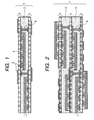
- FIG. 1 An example of the circuit board having built-in electronic parts which is produced by the process in this embodiment is shown in Fig. 1.
- This circuit board has a structure comprising two wiring circuit boards 2 each having an electronic part 1 mounted thereon and a resin layer 3 which is disposed between the circuit boards 2 and in which the electronic parts are embedded.
- the embedding of electronic parts in a resin layer disposed between two wiring circuit boards can eliminate the conventional step of forming spaces for electronic part mounting in an insulating layer of a wiring circuit board. Simplification of steps can hence be attained.
- the wiring circuit boards 2 to be used in this embodiment are not limited as long as they comprise an insulating layer 4 and a conductor layer 5 superposed thereon directly or through an adhesive, and known circuit boards may be used.
- the insulating layer provided in the wiring circuit boards is not particularly limited.
- the insulating layer preferably is a film having a glass transition temperature higher than the curing temperature of the thermosetting resin to be used in the resin layer, which will be described later.
- films of polyimide resins, aramid resins, fluororesins, and poly(ethylene terephthalate) resins are examples of films of polyimide resins, aramid resins, fluororesins, and poly(ethylene terephthalate) resins.
- the conductor layer in the wiring circuit boards is not particularly limited as long as it is one in ordinary use as a conductor layer.
- a copper foil is preferred from the standpoints of ease of processing and cost reduction.
- the conductor layer has been formed so as to have a given wiring pattern including a signal wiring and an electrode, and may have been formed on' one or each side of the insulating layer.
- the formation of the conductor layer so as to have a wiring pattern can be conducted by a known technique such as the subtractive method or additive method.
- Examples of the electronic part 1 include semiconductor elements, resistive elements, and capacitor elements. Such an electronic part can be mounted on the wiring circuit boards by using a known technique, such as flip chip bonding, to bond the electronic part onto the conductor layer formed by the method shown above. In the case where the wiring circuit board has a conductor layer on each side thereof, an electronic part may be mounted on each side of the wiring circuit board.
- the resin to be used for the resin layer 3 is preferably a thermosetting resin, more preferably a polycarbodiimide, from the standpoint of securing heat resistance.
- polycarbodiimide which comprises:
- Symbols a, b, and c each are preferably 0 to 150, more preferably 0 to 100, from the standpoint of realizing high conformability to the recesses and protrusions of electronic parts.
- Symbols d, e, and f each are preferably 0 to 150, more preferably 0 to 100, from the standpoint of realizing high conformability to the recesses and protrusions of electronic parts.
- X preferably represents a single bond or an alkylene group having 1 to 5 carbon atoms.
- alkylene group having 1 to 5 carbon atoms include ethylene and propylene.
- R preferably represents a divalent organic group having 4 to 40 carbon atoms, such as, e.g., an alkylene or arylene group having 4 to 40 carbon atoms.
- alkylene group having 4 to 40 carbon atoms include hexamethylene, a 4,4'-dicyclohexylmethane diisocyanate residue group, and an isophorone diisocyanate residue group.
- arylene group having 4 to 40 carbon atoms include tolylene and a 4,4'-diphenylmethane diisocyanate residue group.
- n 1 , n 2 , and n 3 are as follows.
- the value of n 1 +n 2 is preferably an integer of 2 to 1,000, more preferably an integer of 2 to 100, especially preferably an integer of 2 to 10.
- Symbol n 3 is preferably an integer of 1 to 500, more preferably an integer of 1 to 300, especially preferably an integer of 70 to 100.
- the value of n 1 +n 2 +n 3 is preferably an integer of 70 to 100.
- the value of (n 1 +n 2 )/(n 1 +n 2 +n 3 ) is preferably from 1/15 to 1/3.
- Examples of the terminal structural unit obtained by reacting a monoisocyanate include substituted or unsubstituted aryl or alkyl groups.
- Examples of the substituted aryl groups include tolyl, isopropylphenyl, methoxyphenyl, and chlorophenyl.
- Examples of the unsubstituted aryl groups include phenyl and naphthyl.
- Examples of the substituted alkyl groups include 2,2,4-trimethylhexyl.
- Examples of the unsubstituted alkyl groups include alkyl groups having 1 to 10 carbon atoms, such as n-butyl, n-hexyl, and n-octyl.
- the polycarbodiimide is obtained by subjecting one or more bifunctional liquid rubbers represented by general formula I' : (wherein a, b and c each are an integer of 0 to 200, provided that at least one of a, b and c is not 0, and X represents a single bond or an alkylene group having 1 to 5 carbon atoms) and/or formula II': (wherein d, e and f each are an integer of 0 to 200, provided that at least one of d, e and f is not 0, and X represents a single bond or an alkylene group having 1 to 5 carbon atoms) (these rubbers may be referred to simply as "bifunctional liquid rubbers" in this specification) to a condensation reaction with one or more diisocyanates and then blocking the terminals of the resultant condensate with a monoisocyanate.
- bifunctional liquid rubbers represented by general formula I' : (wherein a, b and c each are an integer of 0 to 200, provided
- Examples of the bifunctional liquid rubber represented by general formula I' include liquid polybutadiene (e.g., Hycar CTB (trademark), manufactured by Ube Industries, Ltd., and C-1000, manufactured by Nippon Soda Co., Ltd.) and liquid polybutadiene/acrylonitrile copolymers (e.g., Hycar CTBN (trademark), manufactured by Ube Industries, Ltd.).
- Examples of the bifunctional liquid rubber represented by general formula II' include liquid hydrogenated polybutadiene (e.g., CI-1000, manufactured by Nippon Soda Co., Ltd.). Each bifunctional liquid rubber may be used singly or two or more bifunctional liquid rubbers may be used in combination.
- diisocyanates to be used as a starting material examples include aromatic diisocyanates and aliphatic diisocyanates. These may be used singly or in a combination of two or more thereof.
- aromatic diisocyanates examples include compounds represented by general formula IV: (wherein X 1 represents an alkyl or alkoxyl group having Ito 5 carbon atoms or a halogen atom), such as 2,4-tolylene diisocyanate, 2,6-tolylene diisocyanate, 6-methoxy-2,4-phenylene diisocyanate, and 5-bromo-2,4-tolylene diisocyanate.
- aliphatic diisocyanates examples include compounds represented by general formula VI: (wherein X 5 and X 6 each represent a single bond or an alkylene group having 1 to 5 carbon atoms and X 7 represents an aliphatic hydrocarbon group having 1 to 8 carbon atoms), such as 4,4'-dicyclohexylmethane diisocyanate, norbornane diisocyanate, 4,4'-cyclohexane diisocyanate, isophorone diisocyanate, methylcyclohexane 2,4-diisocyanate, and 2,4-bis(isocyanatomethyl)cyclohexane.
- general formula VI wherein X 5 and X 6 each represent a single bond or an alkylene group having 1 to 5 carbon atoms and X 7 represents an aliphatic hydrocarbon group having 1 to 8 carbon atoms
- 4,4'-dicyclohexylmethane diisocyanate norbornane diisocyanate
- Examples of the aliphatic diisocyanates further include compounds represented by general formula VII: OCN-X 8 -NCO (wherein X 8 represents an alkylene group having 1 to 18 carbon atoms), such as hexamethylene diisocyanate, 2,2,4-trimethylhexamethylene diisocyanate, octamethylene diisocyanate, and dodecamethylene diisocyanate.
- OCN-X 8 -NCO wherein X 8 represents an alkylene group having 1 to 18 carbon atoms
- Examples of the aliphatic diisocyanates furthermore include compounds represented by general formula VIII: (wherein X 9 and X 10 each represent a single bond or an alkylene group having 1 to 5 carbon atoms), such as xylylene diisocyanate, ⁇ , ⁇ , ⁇ ', ⁇ '-tetramethylxylylene diisocyanate, and 4-isocyanatomethylphenyl isocyanate.
- the bifunctional liquid rubbers respectively represented by general formulae I' and II' are used in such molar amounts as to be capable of satisfying the values of n 1 and n 2 , respectively.
- the molar ratio between these i.e., the ratio of n 1 to n 2 (n 1 /n 2 )
- the molar ratio of the bifunctional liquid rubbers to the diisocyanates is preferably from 1/99 to 1/2, more preferably from 1/10 to 1/2.
- the molar ratio of the aromatic diisocyanate to the aliphatic diisocyanate is preferably from 3/2 to 99/1, more preferably from 4/1 to 99/1.
- Examples of the monoisocyanate to be used as a starting material include isocyanates having a substituted or unsubstituted aryl group, such as phenyl isocyanate, naphthyl isocyanate, tolyl isocyanate, isopropylphenyl isocyanate, methoxyphenyl isocyanate, and chlorophenyl isocyanate; and alkyl isocyanates in which the alkyl has 1 to 10 carbon atoms, such as n-butyl isocyanate, n-hexyl isocyanate, and n-octyl isocyanate. These may be used singly or in a combination of two or more thereof.
- the monoisocyanate be used in an amount of 1 to 40 mol per 100 mol of the diisocyanate ingredient to be used.
- Use of the monoisocyanate ingredient in an amount of 1 mol or larger per 100 mol of the diisocyanate ingredient is preferred because the polycarbodiimide obtained neither has too high a molecular weight nor has undergone crosslinking reaction. Namely, for example, the polycarbodiimide solution obtained undergoes neither an increase in viscosity nor solidification nor a decrease in storage stability.
- the monoisocyanate ingredient in an amount of 40 mol or smaller per 100 mol of the diisocyanate ingredient is preferred because the resultant polycarbodiimide solution has an appropriate viscosity and, for example, film formation by the application and drying of the solution can be satisfactorily conducted.
- the polycarbodiimide solution obtained through terminal blocking with a monoisocyanate used in an amount within that range relative to the amount of the diisocyanate ingredient especially has excellent storage stability.
- the polycarbodiimide is produced by reacting the bifunctional liquid rubber(s) as a starting material with a diisocyanate as another starting material in an aprotic solvent, subsequently subjecting the reaction product to a condensation reaction in the presence of a catalyst for carbodiimide formation to form a carbodiimide, and then blocking the terminals of the carbodiimide with a monoisocyanate.
- the polycarbodiimide production described above is preferably conducted in the following manner.
- toluene solvent 70 parts by weight of the bifunctional liquid rubber is mixed with 30 parts by weight of tolylene diisocyanate. After this mixture is stirred at 50°C for 1 hour, 1-naphthyl isocyanate is mixed therewith in an amount of 2 mol per 100 mol of the tolylene diisocyanate.
- a catalyst for carbodiimide formation is added to the mixture.
- the temperature of the resultant mixture is elevated to 100°C and a carbodiimide-forming reaction is conducted at this temperature for about 2 hours to produce a polycarbodiimide.
- the end point of the carbodiimide-forming reaction can be determined, for example, by the method which will be described later.
- the temperature for the reaction between the bifunctional liquid rubber and the diisocyanate is preferably 10 to 50°C, more preferably 30 to 50°C, from the standpoints of reaction time reduction and the prevention of thermal deterioration of the liquid rubber.
- the reaction time may be about from 30 minutes to 2 hours, and is usually about 1 hour.
- the end point of the reaction is ascertained from the disappearance of absorption by the OH stretching vibration (3,000 cm -1 ) attributable to the terminal carboxyl groups of the bifunctional liquid rubber.
- the temperature for the carbodiimide-forming reaction is preferably 10 to 150°C, more preferably 40 to 110°C.
- Carbodiimide-forming reaction temperatures not lower than 10°C are preferred because the reaction does not necessitate too long a time and gives a polycarbodiimide solution having no functional isocyanate groups remaining therein.
- This polycarbodiimide solution for example, has improved storage stability.
- Reaction temperatures not higher than 150°C are preferred because the reaction does not proceed too rapidly and side reactions do not cause gelation, and because this, for example, results in a polycarbodiimide solution having improved storage stability.
- Examples of the catalyst for carbodiimide formation include 3-methyl-1-phenyl-2-phospholene 1-oxide, 1-phenyl-2-phospholene 1-oxide, 1-phenyl-2-phospholene 1-sulfide, 1-ethyl-3-methyl-2-phospholene 1-oxide, 3-methyl-1-phenyl-1-phospha-3-cyclopentene 1-oxide, 2,5-dihydro-3-methyl-1-phenylphospholene 1-oxide, and the 3-phospholene isomers of these.
- phosphine oxides such as triphenylphosphine oxide, tritolylphosphine oxide, and bis(oxadiphenylphosphino)ethane. These may be used singly or in a combination of two or more thereof.
- the catalyst for carbodiimide formation be used in an amount in the range of 0.001 to 5 mol per 100 mol of all isocyanate ingredients to be used. Amounts of the catalyst not smaller than 0.001 mol are preferred because the reaction does not necessitate too long a time. Amounts thereof not larger than 5 mol are preferred because the gelation causative of too high a reaction rate does not occur and this, for example, results in an improvement in the storage stability of the polycarbodiimide solution.
- the terminal blocking with a monoisocyanate can be accomplished by adding the monoisocyanate to the reaction mixture in an initial, middle, or final stage of carbodiimide formation or throughout the carbodiimide formation.
- Examples of the aprotic solvent to be used for producing the polycarbodiimide include toluene, xylene, alkyltoluenes in which the alkyl has 3 to 5 carbon atoms, benzene, alkylbenzenes in which the alkyl has 3 to 6 carbon atoms, naphthalene, tetrahydrofuran, dioxane, acetone, butanone, cyclohexanone, N-methylpyrrolidone, N,N-dimethylformamide, and N,N-dimethylacetamide. These may be used singly or in a combination of two or more thereof.
- the aprotic solvent be used in such an amount that the polycarbodiimide concentration in the resultant polycarbodiimide solution is in the range of 1 to 90% by weight.
- Polycarbodiimide concentrations not lower than 1% by weight are preferred because solvent removal in the molding of the polycarbodiimide obtained is easy.
- Polycarbodiimide concentrations not higher than 90% by weight are preferred because the polycarbodiimide solution has a moderate viscosity and improved storage stability.
- IR analysis infrared spectroscopy
- a polycarbodiimide is obtained usually in the form of a solution.
- the solution obtained may be poured into a poor solvent such as methanol, ethanol, isopropyl alcohol, or hexane to precipitate the polycarbodiimide and remove the unreacted monomers and the catalyst.
- the precipitate is washed and dried in a given manner and then dissolved again in an aprotic solvent. By performing this operation, the polycarbodiimide solution can have improved storage stability.
- the solution may be purified, for example, by adsorptively removing the by-products with an appropriate adsorbent.
- the adsorbent include alumina gel, silica gel, activated carbon, zeolites, activated magnesium oxide, activated bauxite, Fuller's earth, activated clay, and molecular sieve carbon. These may be used singly or in a combination of two or more thereof.
- the resin thus obtained which comprises a polycarbodiimide, has a curing temperature of preferably 120 to 250°C and a glass transition temperature of preferably 150 to 250°C.
- the resin layer to be used in this embodiment comprises the thermosetting resin in an amount of generally 10 to 100% by weight, preferably 30 to 100% by weight.
- the resin layer in this embodiment is preferably used as a resin film, although the form of the resin to be used is not particularly limited.
- the film is obtained by dissolving the polycarbodiimide in any of the aprotic solvents enumerated above, such as toluene or cyclohexanone, applying the resultant solution to a substrate by a known technique, e.g., casting, spin coating, or roll coating, and drying the coating with heating.
- the application of the solution is preferably conducted in such an amount as to give a film having a thickness of 10 to 300 ⁇ m.
- the substrate may be any film having heat resistance and chemical resistance. Examples thereof include films of polyimides, polyesters, and poly(ethylene terephthalate). These polymers may be used singly or in a combination of two or more thereof.
- the film to be used as the substrate preferably is one which has been treated with a release agent such as, e.g., a fluorinated silicone.
- the drying with heating of the polycarbodiimide solution applied to the substrate is preferably conducted under such temperature and time conditions that the solvent can be removed, for the purpose of drying the solution without causing the curing reaction of the polycarbodiimide to proceed excessively.
- the drying temperature is preferably 30 to 200°C, more preferably 50 to 175°C, especially preferably 70 to 150°C. Drying temperatures not lower than 30°C are preferred because the resultant resin film contains no residual solvent and has high reliability. Drying temperatures not higher than 200°C are preferred because the resin film can be sufficiently dried while being inhibited from thermally curing.
- the time period of drying is preferably from 30 seconds to 30 minutes, more preferably 1 to 10 minutes, especially preferably 2 to 5 minutes. Drying times not shorter than 30 seconds are preferred because the resultant resin film contains no residual solvent and has high reliability. Drying times not longer than 30 minutes are preferred because the resin film can be sufficiently dried while being inhibited from thermally curing.
- various nonconductive inorganic powders e.g., powders of ceramics such as alumina, silica, magnesia, and silicon nitride, may be incorporated according to need for the purpose of modulus regulation, etc.
- powders may be used singly or in a combination of two or more thereof.
- the resin film may suitably further contain an inorganic filler as long as this does not impair the processability and heat resistance of the layer.
- various additives such as a leveling agent or defoamer for obtaining surface smoothness, a silane coupling agent or titanate coupling agent for improving adhesion, a nonionic surfactant, a fluorochemical surfactant, and a silicone additive may have been added according to need.
- the amount of these additives to be added is preferably 0.1 to 100 parts by weight, more preferably 0.2 to 50 parts by weight, per 100 parts by weight of the polycarbodiimide.
- Conduction paths 6 may be formed in the resin film in order to electrically connect the wirings of the wiring circuit boards to each other.
- the conduction paths are formed, for example, by forming through-holes extending in the direction of the thickness of the resin film by means of a laser, punching, drilling, etc. and filling the through-holes with a paste containing metal particles, e.g., copper particles or silver particles, by means of a dispenser, suction, screen printing, etc.
- the circuit board 7 having built-in electronic parts is produced by disposing two wiring circuit boards 2 each having an electronic part 1 mounted thereon so that the electronic-part-mounting sides of the respective circuit boards face each other, disposing a resin layer 3 between the circuit boards, and press-bonding the resin layer to the circuit boards, for example, by vacuum pressing.
- the press-bonding of the resin layer to the circuit boards is conducted at a pressure of preferably 9.8 ⁇ 10 -3 to 9.8 ⁇ 10 -1 MPa, more preferably 9.8 ⁇ 10 -2 to 4.9 ⁇ 10 -1 MPa, with heating at preferably 100 to 200°C, more preferably 140 to 170°C, for preferably from 5 seconds to 10 minutes, more preferably from 10 seconds to 1 minute.
- the electronic parts are embedded in the resin layer and the wiring circuit boards are electrically connected to each other by the conduction paths in the direction of superposition.
- a wiring circuit board having an electronic part mounted thereon and a resin layer may be further superposed on the circuit board having built-in electronic parts produced above, as shown in Fig. 2.
- the number of circuit boards to be superposed may be adjusted according to the intended use.
- the resultant structure is preferably further heated at a temperature of about 120 to 200°C for about 1 to 5 hours in order to completely cure the polycarbodiimide in the resin layer.
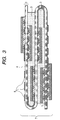
- the process for producing a circuit board having built-in electronic parts in another embodiment of the invention comprises the steps of: folding a wiring circuit board having two or more electronic parts mounted thereon; disposing a resin layer in the resultant space between sections of the folded circuit board where electronic-part-mounting sides have come to face each other; and press-bonding the resin layer to the folded sections of the circuit board.
- FIG. 3 An example of the circuit board having built-in electronic parts which is produced by the process in this embodiment is shown in Fig. 3.
- This circuit board has a structure comprising: a wiring circuit board 2 which has two or more electronic parts 1 mounted thereon and has been folded; and a resin layer 3 which has been disposed between the folded sections of the circuit board and in which the electronic parts 1 have been embedded.
- the number of folds of the wiring circuit board may be determined according to the intended use.
- the wiring circuit board, electronic parts, and resin layer to be used may be the same as those described for the above-described embodiments.
- this process does not necessitate the formation of a conduction path in a resin layer for electrically connecting the wirings of wiring circuit boards, because only one common wiring circuit board is used.
- the circuit board 7 having built-in electronic parts is produced by preparing a wiring circuit board 2 having two or more electronic parts 1 mounted thereon, disposing a resin layer 3 in given positions on electronic-part-mounting sides, folding the wiring circuit board 2 so that the electronic-part-mounting sides face each other, and press-bonding the resin layer to the circuit board, for example, by vacuum pressing.
- the disposition of the resin layer on the wiring circuit board may be conducted by a method in which through-holes for positioning are formed beforehand in the circuit board and the resin film, and pins for positioning are used to dispose the resin film.
- the press-bonding of the resin layer to the circuit board is conducted at a pressure of preferably 9.8 ⁇ 10 -3 to 9.8 ⁇ 10 -1 MPa, more preferably 9.8 ⁇ 10 -2 to 4.9 ⁇ 10 -1 MPa, with heating at preferably 100 to 200°C, more preferably 140 to 170°C, for preferably from 5 seconds to 10 minutes, more preferably from 10 seconds to 1 minute.
- the electronic parts are embedded in the resin layer.
- circuit board and a resin layer may be further superposed on the circuit board having built-in electronic parts produced in this embodiment.
- Such a circuit board having built-in electronic parts may be produced according to the intended use.
- the resultant structure is preferably further heated at a temperature of about 120 to 200°C for about 1 to 5 hours in order to completely cure the polycarbodiimide in the resin layer.
- n 1 +n 2 was 3 to 5
- n 3 was 71 to 91
- n 1 +n 2 +n 3 was 74 to 96
- (n 1 +n 2 ) / (n 1 +n 2 +n 3 ) was from 5/74 to 3/96.
- the polycarbodiimide solution obtained was applied with a roll coater on a separator (thickness, 50 ⁇ m; manufactured by Mitsubishi Polyester Film Corp.) consisting of a poly(ethylene terephthalate) film treated with a release agent (fluorinated silicone), in such an amount as to give a resin film having a thickness of 250 ⁇ m.
- a separator thinness, 50 ⁇ m; manufactured by Mitsubishi Polyester Film Corp.
- a release agent fluorinated silicone
- Through-holes of 0.3 mm-diameter were formed by punching in the resin film obtained. These through-holes were filled with a paste containing copper particles by means of a dispenser to form conduction paths.
- a double-sided copper-clad substrate was prepared which comprised a polyimide resin as an insulating layer and a copper foil superposed as a conductor layer on each side of the insulating layer.
- the copper foils were etched to produce a wiring circuit board having a given wiring pattern on each side. Two such wiring circuit boards were prepared.
- a semiconductor element having a thickness of 100 ⁇ m was mounted with a flip chip bonder on one side of each of the two wiring circuit boards.
- the process of the invention is usable in the production of electronic appliances which necessitate the high-density mounting of electronic parts such as semiconductor elements.
Landscapes
- Engineering & Computer Science (AREA)
- Manufacturing & Machinery (AREA)
- Microelectronics & Electronic Packaging (AREA)
- Laminated Bodies (AREA)
- Polyurethanes Or Polyureas (AREA)
- Combinations Of Printed Boards (AREA)
- Production Of Multi-Layered Print Wiring Board (AREA)
Applications Claiming Priority (2)
| Application Number | Priority Date | Filing Date | Title |
|---|---|---|---|
| JP2004010372A JP2005203674A (ja) | 2004-01-19 | 2004-01-19 | 電子部品内蔵基板の製造方法 |
| JP2004010372 | 2004-01-19 |
Publications (2)
| Publication Number | Publication Date |
|---|---|
| EP1555862A2 true EP1555862A2 (de) | 2005-07-20 |
| EP1555862A3 EP1555862A3 (de) | 2007-08-08 |
Family
ID=34616935
Family Applications (1)
| Application Number | Title | Priority Date | Filing Date |
|---|---|---|---|
| EP05001025A Withdrawn EP1555862A3 (de) | 2004-01-19 | 2005-01-19 | Verfahren zur Herstellung einer Leiterplatte mit eingebautem elektronischem Bauteil |
Country Status (4)
| Country | Link |
|---|---|
| US (1) | US20050158911A1 (de) |
| EP (1) | EP1555862A3 (de) |
| JP (1) | JP2005203674A (de) |
| KR (1) | KR20050076646A (de) |
Families Citing this family (11)
| Publication number | Priority date | Publication date | Assignee | Title |
|---|---|---|---|---|
| JP4619807B2 (ja) * | 2004-01-30 | 2011-01-26 | パナソニック株式会社 | 部品内蔵モジュールおよび部品内蔵モジュールを備えた電子機器 |
| JP4285339B2 (ja) * | 2004-06-15 | 2009-06-24 | パナソニック株式会社 | 回路モジュールおよび回路モジュールの製造方法 |
| US20060223227A1 (en) * | 2005-04-04 | 2006-10-05 | Tessera, Inc. | Molding method for foldover package |
| US7767543B2 (en) * | 2005-09-06 | 2010-08-03 | Semiconductor Energy Laboratory Co., Ltd. | Method for manufacturing a micro-electro-mechanical device with a folded substrate |
| TW200721216A (en) * | 2005-09-22 | 2007-06-01 | Murata Manufacturing Co | Packaging method of electronic component module, method for manufacturing electronic apparatus using it, and electronic component module |
| JP2009016626A (ja) * | 2007-07-06 | 2009-01-22 | Panasonic Corp | 半導体モジュール装置および半導体モジュール装置の製造方法ならびにフラットパネル型表示装置,プラズマディスプレイパネル |
| US20110105079A1 (en) * | 2007-11-14 | 2011-05-05 | Mark Randall Levea | Liberty phone and liberty phone system |
| JP2011035345A (ja) * | 2009-08-06 | 2011-02-17 | Fujitsu Ltd | 半導体素子モジュール、電子回路ユニット、電子デバイス、及び、半導体素子モジュールの製造方法 |
| JP7044007B2 (ja) * | 2018-07-31 | 2022-03-30 | 株式会社オートネットワーク技術研究所 | 回路構成体 |
| CN115315071B (zh) * | 2021-05-07 | 2025-12-12 | 鹏鼎控股(深圳)股份有限公司 | 内埋元件电路板及其制造方法 |
| CN117602159B (zh) * | 2024-01-23 | 2024-04-05 | 四川英创力电子科技股份有限公司 | 一种带有覆膜功能的电路板自动投板装置及方法 |
Family Cites Families (10)
| Publication number | Priority date | Publication date | Assignee | Title |
|---|---|---|---|---|
| JPS62155546A (ja) * | 1985-12-27 | 1987-07-10 | Toshiba Corp | メモリ−モジユ−ル |
| JPH02164096A (ja) * | 1988-12-19 | 1990-06-25 | Matsushita Electric Ind Co Ltd | 多層電子回路基板とその製造方法 |
| JP3733153B2 (ja) * | 1994-11-24 | 2006-01-11 | 日清紡績株式会社 | 多層プリント配線板 |
| US6180261B1 (en) * | 1997-10-21 | 2001-01-30 | Nitto Denko Corporation | Low thermal expansion circuit board and multilayer wiring circuit board |
| JP2001217388A (ja) * | 2000-02-01 | 2001-08-10 | Sony Corp | 電子装置およびその製造方法 |
| JP2002171071A (ja) * | 2000-12-04 | 2002-06-14 | Ibiden Co Ltd | 多層配線基板、及びその製造方法 |
| FR2822338B1 (fr) * | 2001-03-14 | 2003-06-27 | Sagem | Procede pour connecter electriquement des plots de contact d'un composant microelectronique directement a des pistes de circuits imprimes, et plaque a circuits imprimes ainsi constituee |
| TW550997B (en) * | 2001-10-18 | 2003-09-01 | Matsushita Electric Industrial Co Ltd | Module with built-in components and the manufacturing method thereof |
| TW200302685A (en) * | 2002-01-23 | 2003-08-01 | Matsushita Electric Industrial Co Ltd | Circuit component built-in module and method of manufacturing the same |
| JP2004269691A (ja) * | 2003-03-07 | 2004-09-30 | Nitto Denko Corp | ポリカルボジイミド共重合体およびその製造方法 |
-
2004
- 2004-01-19 JP JP2004010372A patent/JP2005203674A/ja active Pending
-
2005
- 2005-01-18 KR KR1020050004540A patent/KR20050076646A/ko not_active Withdrawn
- 2005-01-19 US US11/037,018 patent/US20050158911A1/en not_active Abandoned
- 2005-01-19 EP EP05001025A patent/EP1555862A3/de not_active Withdrawn
Also Published As
| Publication number | Publication date |
|---|---|
| US20050158911A1 (en) | 2005-07-21 |
| JP2005203674A (ja) | 2005-07-28 |
| EP1555862A3 (de) | 2007-08-08 |
| KR20050076646A (ko) | 2005-07-26 |
Similar Documents
| Publication | Publication Date | Title |
|---|---|---|
| US6420018B1 (en) | Low thermal expansion circuit board and multilayer wiring circuit board | |
| CN101189926B (zh) | 多层配线板 | |
| CN100394599C (zh) | 加工精度良好的半导体模块及其制造方法和半导体装置 | |
| US6492484B2 (en) | Polycarbodiimide | |
| US20100025093A1 (en) | Multilayered circuit board and semiconductor device | |
| EP1555862A2 (de) | Verfahren zur Herstellung einer Leiterplatte mit eingebautem elektronischem Bauteil | |
| KR101339510B1 (ko) | 인쇄회로기판용 수지조성물 및 이를 포함하는 인쇄회로기판 | |
| KR20020074416A (ko) | 이방성 도전 필름 | |
| KR101409048B1 (ko) | 회로 기판의 제조 방법, 반도체 제조 장치, 회로 기판 및 반도체 장치 | |
| EP1598908A2 (de) | Optische Halbleitervorrichtung | |
| US5891540A (en) | Adhesive tape for electronic parts | |
| US7487586B2 (en) | Process for producing semiconductor device | |
| JP2004111945A (ja) | 配線基板及びその製造方法 | |
| JP2002261453A (ja) | 多層配線基板 | |
| US20040096633A1 (en) | Adhesive film for underfill and semiconductor device using the same | |
| US20040178423A1 (en) | Adhesive film for underfill and semiconductor device using the same | |
| EP1512706A2 (de) | Wärmehartbares Harz | |
| CN1930219B (zh) | 预浸体、贴金属箔层叠板及使用它们的印刷电路板 | |
| JP2003347454A (ja) | 多層配線基板 | |
| JPH08148838A (ja) | 多層プリント配線板及びその製造方法 | |
| JP2005116624A (ja) | 半導体素子の実装方法 | |
| JP2002265887A (ja) | アンダーフィル用接着フィルム及びこれを用いた半導体装置 | |
| JP2006190717A (ja) | 半導体集積回路用基板 | |
| JP2003046259A (ja) | 多層配線基板 | |
| JP2003174264A (ja) | 絶縁フィルムおよびこれを用いた多層配線基板 |
Legal Events
| Date | Code | Title | Description |
|---|---|---|---|
| PUAI | Public reference made under article 153(3) epc to a published international application that has entered the european phase |
Free format text: ORIGINAL CODE: 0009012 |
|
| AK | Designated contracting states |
Kind code of ref document: A2 Designated state(s): AT BE BG CH CY CZ DE DK EE ES FI FR GB GR HU IE IS IT LI LT LU MC NL PL PT RO SE SI SK TR |
|
| AX | Request for extension of the european patent |
Extension state: AL BA HR LV MK YU |
|
| PUAL | Search report despatched |
Free format text: ORIGINAL CODE: 0009013 |
|
| AK | Designated contracting states |
Kind code of ref document: A3 Designated state(s): AT BE BG CH CY CZ DE DK EE ES FI FR GB GR HU IE IS IT LI LT LU MC NL PL PT RO SE SI SK TR |
|
| AX | Request for extension of the european patent |
Extension state: AL BA HR LV MK YU |
|
| STAA | Information on the status of an ep patent application or granted ep patent |
Free format text: STATUS: THE APPLICATION IS DEEMED TO BE WITHDRAWN |
|
| 18D | Application deemed to be withdrawn |
Effective date: 20070801 |