EP1560149A2 - Terminal portable de traitement d'informations - Google Patents
Terminal portable de traitement d'informations Download PDFInfo
- Publication number
- EP1560149A2 EP1560149A2 EP05250483A EP05250483A EP1560149A2 EP 1560149 A2 EP1560149 A2 EP 1560149A2 EP 05250483 A EP05250483 A EP 05250483A EP 05250483 A EP05250483 A EP 05250483A EP 1560149 A2 EP1560149 A2 EP 1560149A2
- Authority
- EP
- European Patent Office
- Prior art keywords
- antenna coil
- circuit
- portable type
- terminal device
- information processing
- Prior art date
- Legal status (The legal status is an assumption and is not a legal conclusion. Google has not performed a legal analysis and makes no representation as to the accuracy of the status listed.)
- Granted
Links
Images





Classifications
-
- E—FIXED CONSTRUCTIONS
- E04—BUILDING
- E04B—GENERAL BUILDING CONSTRUCTIONS; WALLS, e.g. PARTITIONS; ROOFS; FLOORS; CEILINGS; INSULATION OR OTHER PROTECTION OF BUILDINGS
- E04B2/00—Walls, e.g. partitions, for buildings; Wall construction with regard to insulation; Connections specially adapted to walls
- E04B2/02—Walls, e.g. partitions, for buildings; Wall construction with regard to insulation; Connections specially adapted to walls built-up from layers of building elements
- E04B2/04—Walls having neither cavities between, nor in, the solid elements
- E04B2/06—Walls having neither cavities between, nor in, the solid elements using elements having specially-designed means for stabilising the position
- E04B2/10—Walls having neither cavities between, nor in, the solid elements using elements having specially-designed means for stabilising the position by filling material with or without reinforcements in small channels in, or in grooves between, the elements
-
- G—PHYSICS
- G06—COMPUTING OR CALCULATING; COUNTING
- G06K—GRAPHICAL DATA READING; PRESENTATION OF DATA; RECORD CARRIERS; HANDLING RECORD CARRIERS
- G06K7/00—Methods or arrangements for sensing record carriers, e.g. for reading patterns
- G06K7/10—Methods or arrangements for sensing record carriers, e.g. for reading patterns by electromagnetic radiation, e.g. optical sensing; by corpuscular radiation
- G06K7/10009—Methods or arrangements for sensing record carriers, e.g. for reading patterns by electromagnetic radiation, e.g. optical sensing; by corpuscular radiation sensing by radiation using wavelengths larger than 0.1 mm, e.g. radio-waves or microwaves
- G06K7/10316—Methods or arrangements for sensing record carriers, e.g. for reading patterns by electromagnetic radiation, e.g. optical sensing; by corpuscular radiation sensing by radiation using wavelengths larger than 0.1 mm, e.g. radio-waves or microwaves using at least one antenna particularly designed for interrogating the wireless record carriers
-
- G—PHYSICS
- G06—COMPUTING OR CALCULATING; COUNTING
- G06K—GRAPHICAL DATA READING; PRESENTATION OF DATA; RECORD CARRIERS; HANDLING RECORD CARRIERS
- G06K7/00—Methods or arrangements for sensing record carriers, e.g. for reading patterns
- G06K7/0008—General problems related to the reading of electronic memory record carriers, independent of its reading method, e.g. power transfer
-
- G—PHYSICS
- G06—COMPUTING OR CALCULATING; COUNTING
- G06K—GRAPHICAL DATA READING; PRESENTATION OF DATA; RECORD CARRIERS; HANDLING RECORD CARRIERS
- G06K7/00—Methods or arrangements for sensing record carriers, e.g. for reading patterns
- G06K7/10—Methods or arrangements for sensing record carriers, e.g. for reading patterns by electromagnetic radiation, e.g. optical sensing; by corpuscular radiation
- G06K7/10009—Methods or arrangements for sensing record carriers, e.g. for reading patterns by electromagnetic radiation, e.g. optical sensing; by corpuscular radiation sensing by radiation using wavelengths larger than 0.1 mm, e.g. radio-waves or microwaves
- G06K7/10316—Methods or arrangements for sensing record carriers, e.g. for reading patterns by electromagnetic radiation, e.g. optical sensing; by corpuscular radiation sensing by radiation using wavelengths larger than 0.1 mm, e.g. radio-waves or microwaves using at least one antenna particularly designed for interrogating the wireless record carriers
- G06K7/10336—Methods or arrangements for sensing record carriers, e.g. for reading patterns by electromagnetic radiation, e.g. optical sensing; by corpuscular radiation sensing by radiation using wavelengths larger than 0.1 mm, e.g. radio-waves or microwaves using at least one antenna particularly designed for interrogating the wireless record carriers the antenna being of the near field type, inductive coil
Definitions
- This invention relates to a portable type information processing terminal device.
- Embodiments of the present invention relate to a portable type information processing terminal device containing an integrated circuit element of a non-contact communication system such as an RFID (radio frequency identification) system.
- a non-contact communication system such as an RFID (radio frequency identification) system.
- So-called RFID systems adapted to use a non-contact type IC card are known in the field of automatic check gates of railway stations, security systems for checking persons going into and out of buildings and electronic money systems and the like.
- An RFID system typically comprises one or more than one non-contact type IC card and a reader/writer for writing data on and reading data from the non-contact type IC card.
- the antenna coil of the reader/writer and that of the IC card are magnetically coupled to each other by inductive coupling to allow a non-contact data communication to take place between the IC card and the reader/writer.
- Data can be exchanged easily and rapidly in such an RFID system because it is no longer necessary to insert an IC card into a reader/writer or contact an IC card to a metal contact as in the case of conventional contact type IC card systems. Additionally, electric power is supplied to the non-contact type IC card as the AC magnetic field that is excited by the antenna coil of the reader/writer is applied to the IC card. In other words, the IC card is not required to contain a power source such as a battery in the inside and operates highly reliably so that it needs only easy maintenance services.
- a reader/writer is installed in a portable type information processing terminal device such as PDA (personal digital assistants) and the portable type information processing terminal device is adapted to read data from the non-contact type IC card and update the data (see Patent Document 1: Jpn. Pat. Appln. Laid-Open Publication No. 2001-307032).
- a portable type information processing terminal device such as a PDA or a portable type telephone set is designed so as to be constantly carried by the user when the user goes out. Therefore, if a portable type information processing terminal device is provided with the functional feature of a non-contact type IC card, the user of the portable type information processing terminal device who always carries it does not have to carry any other non-contact type IC card to a great advantage on the part of the user.
- portable type information processing terminal devices are compact but multifunctional, metal parts are highly densely mounted in a small cabinet thereof.
- the printed circuit board such a device has an electrically conductive multilayer structure and electronic parts such as integrated circuit elements are highly densely mounted on the multilayer printed circuit board.
- a portable type information processing terminal device contains a battery pack as power source of the device.
- the battery pack contains a metal as a material of a frame or the like.
- the resonance frequency of the antenna coil can be remarkably modified under the influence of the metal parts mounted in the cabinet to make it difficult to regulate the resonance frequency of the antenna coil and at the same time to secure the card voltage for driving at least the signal processing integrated circuit element connected to the antenna coil.
- the antenna coil and the signal processing integrated circuit element of an RFID system are mounted not on the substrate where the antenna coil is arranged but on the main substrate of the portable type information processing terminal device, the antenna coil and the signal processing integrated circuit element are separated from each other by a long distance. As the antenna coil and the signal processing integrated circuit element are separated from each other by a long distance, the resistance between the antenna coil and the signal processing integrated circuit element rises to give rise to a large loss. Furthermore, the performance of the device is degraded in terms of anti-external-noise performance.
- a portable type information processing terminal device it is not possible for a portable type information processing terminal device to reliably transmit and receive data by simply arranging a non-contact type IC card in the device.
- Patent Document 2 Jpn. Pat. Appln. Laid-Open Publication No. 2003-87385 describes a technique that may appear to resemble embodiments of the present invention.
- the portable type telephone set described in Patent Document 2 is characterized by arranging an RFID tag on an antenna and hence is different from a portable type information processing terminal device according to embodiments of the invention in which an RFID tag contained in a cabinet.
- Embodiments of the present invention seek to provide a novel portable type information processing terminal device having the functional feature of a portable type IC card.
- Embodiments of the present invention seek to provide a portable type information processing terminal device of which the resonance frequency of the antenna coil can be roughly regulated with ease.
- Embodiments of the present invention seek to provide a portable type information processing terminal device that can minimize the influence of the metal parts mounted in the cabinet thereof when it is configured to contain a portable type IC card in the cabinet.
- Embodiments of the present invention seek to provide a portable type information processing terminal device that operates excellently in terms of anti-extemal-noise performance when a portable type IC card is arranged in the cabinet.
- a portable type information processing terminal device comprises: a substrate carrying a substantially annular antenna coil thereon; a signal processing integrated circuit element arranged inside or near the antenna coil; a magnetic plate arranged on the substrate; and a metal plate arranged on the magnetic plate; the substrate, the magnetic plate and the metal plate being integrally formed and arranged in a cabinet.
- a portable type information processing terminal device can be downsized and made lightweight as the signal processing integrated circuit element of the device is arranged inside or near the antenna coil.
- a portable type information processing terminal device can be made very thin as a result of integrally forming the substrate, the magnetic plate and the metal plate.
- the portable type telephone set 1 comprises an equipment main body 2 and a panel section 3 rotatably fitted to the equipment main body 2.
- the equipment main body 2 has a substantially rectangular profile and, an input section 2a including ten keys, a communication button, a power supply button and other push buttons, a microphone 2b for receiving sound as input and transforming the input sound into an electric signal and an RFID section 2c including a transmission/reception section and other sections of an RFID system are arranged on one of the main surfaces thereof.
- the microphone 2b is arranged at an end of the main surface and hence near the other main surface of the equipment main body 2 at the rear side thereof so that it may be located near the mouth of the user.
- the RFID section 2c is also arranged at the end of the main surface and hence near the rear side of the equipment main body 2.
- the equipment main body 2 is provided at the rear side thereof with a battery inlet port 2d through which a battery pack 4 that operates as power source of the portable type telephone set 1 is put in and also with a battery receiving section 2e that is directly connected to the battery inlet port 2d to receive the battery pack 4.
- the battery pack 4 typically contains a lithium ion secondary battery.
- the battery pack 4 has, for example, a substantially rectangular profile and formed by a metal material such as aluminum.
- the RFID section 2c is formed on the main surface of the equipment main body 2 that takes the role of operation panel and the battery receiving section 2e is formed on the other main surface to receive the battery pack 4.
- the panel section 3 that is fitted to the equipment main body 2 can be turned in the sense of arrow R in FIG. 1.
- a display section 3a including an LCD (liquid crystal display), an organic EL (electroluminescent) display or some other display and a speaker 3b adapted to transform an electric signal into reproduced sound are arranged on the main surface of the panel section 3 that faces the equipment main body 2.
- a communication antenna for communicating with a base station is arranged on the front side of the panel section 3.
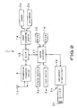
- the portable type telephone set 1 comprises a transmission/reception section 9connected to a communication antenna 11 to communicate with a base station, a DSP (digital signal processor) 13 connected to the transmission/reception section 12 to modulate/demodulate signals for voice communications and signal communications, a sound processing section 14 for transforming the digital signal of sound data received at the time of communication into an analog signal and outputting it to the speaker 3b and also transforming the analog signal of sound data input from the microphone 2b into a digital signal, a ROM (read only memory) 15 storing a control program and so on, a RAM (random access memory) 16 into which the control program and so on stored in the ROM 15 are loaded and a system controller 17 for controlling the entire operation of the portable type telephone set 1.
- a DSP digital signal processor
- the transmission/reception section 12 performs a processing operation of frequency conversion on the sound data input from the DSP 13 and transmits the sound data obtained as a result of the processing operation to the base station by way of the communication antenna 11.
- the transmission/reception section 12 amplifies the RF signal received by way of the communication antenna 8 and performs a processing operation of frequency conversion on the RF signal and outputs the obtained data to the DSP 13.
- the transmission/reception section 12 is adapted to communications conforming to the PDC (Personal Digital Cellular) System, the IMT (International Mobile Telecommunication)-2000 System, the DS-CDMA (Direct Spread Code Division Multiple Access) System or the like.
- the DSP 13 decodes the sound data that are typically subjected to spread spectrum and input from the transmission/reception section 12 and outputs the decoded sound data to the speaker 3b.
- the DSP 13 performs an operation of spread spectrum on the sound data input from the DSP 13 [the sound processing section 14?] and outputs the sound data to the transmission/reception section 12.
- the DSP 13 outputs the decoded data to the system controller 17 and encodes the data input from the system controller 17.
- the sound processing section 14 transforms the electric analog signal that corresponds to the user's voice collected by the microphone 2b into a digital signal and outputs it to the DSP 13.
- the sound processing section 14 also transforms the digital signal of the sound data input from the DSP 13 into an analog signal and output it to the speaker 3c.
- the system controller 17 loads the program read out from the ROM 15 according to the operation signal that is input from the input section 2a in the RAM 16, performs a necessary operation on it and outputs information on the situation of the operation to the display section 3a.
- the system controller 17 also outputs control data and the like to the DSP 13.
- the system controller 17 is also connected to an RFID section 2c.
- the RFID section 2c has a non-contact type IC card circuit 18 on which data are written and from which data are read by an external reader/writer.
- the RFID section 2c has an antenna coil 21 formed by flatly winding a conductor wire in order to communicate with the reader/writer and a capacitor 22 connected in parallel with the antenna coil 21 so that the antenna coil 21 and the capacitor 22 form a parallel resonance circuit.
- Data are transmitted and received as the antenna coil of the external reader/writer and the antenna coil 21 are coupled to each other by inductive coupling. More specifically, since the antenna coil 21 is a loop antenna, it radiates an electromagnetic wave to the outside as the electric current flowing through the closed loop changes.
- the density of the magnetic flux passing through the closed loop changes and an electric current flows through the closed loop as a function of the intensity of the electromagnetic wave or the magnetic field.
- the non-contact type IC card circuit 18 includes a rectifying circuit 23 for rectifying and smoothing the electric signal supplied from the antenna coil 21, a regulator 24 for generating a DC voltage, an HPF (high-pass filter) 25 for extracting a high frequency component of the electric signal output from the rectifying circuit 23, a demodulation circuit 26 for demodulating the high frequency component signal input from the HPF 25, a sequencer 27 for controlling the operation of writing or reading data according to the data supplied from the demodulation circuit 26, a memory 28 for storing the data supplied from the demodulation circuit 26 and a modulation circuit 29 for modulating the data to be transmitted.
- a rectifying circuit 23 for rectifying and smoothing the electric signal supplied from the antenna coil 21, a regulator 24 for generating a DC voltage, an HPF (high-pass filter) 25 for extracting a high frequency component of the electric signal output from the rectifying circuit 23, a demodulation circuit 26 for demodulating the high frequency component signal input from the HPF 25, a sequencer 27 for controlling the operation of writing or reading data
- the rectifying circuit 23 includes a diode 23a, a resistor 23b and a capacitor 23c.
- the diode 23a has its anode terminal connected to an end of the capacitor 22 and the antenna coil 21, and its cathode terminal connected to an end of the resistor 23b and the capacitor 23c.
- the other end of the resistor 23b and the capacitor 23c is connected to the other end of the capacitor 22 and the antenna coil 21.
- the rectifying circuit 23 rectifies and smoothes the electric signal supplied from the antenna coil 21 and outputs it to the regulator 24 and the HPF 25.
- the regulator 24 generates a DC voltage. More specifically, the regulator 24 generates a DC voltage from the energy of the output signal of the rectifying circuit 23 or from the energy of an external power source, which may be the battery pack 4. Then, the regulator 24 supplies the DC voltage to the electric circuit of the sequencer 27.
- the HPF 25 has a capacitor 25a and a resistor 25b. It extracts, or detects, a high frequency component of the electric signal supplied from the rectifying circuit 23 and outputs it to the demodulation circuit 26.
- the demodulation circuit 26 is connected to an end of the capacitor 25a of the HPF 25 and to the other end of the resistor 25b. It demodulates the signal of the high frequency component input from the HPF 25 and outputs it to the sequencer 26. More specifically, the demodulation circuit 38 demodulates the data modulated by means of Manchester codes, a modified mirror or an NRZ (Non Return to Zero) technique or the like.
- the sequencer 27 includes a ROM, RAM or the like and is connected to the demodulation circuit 26.
- the sequencer 27 executes a program stored in the ROM according to the commend input from the demodulation circuit 26 and reads out data stored in the memory 28 based on the executed program, or writes data supplied from the demodulation circuit 26 into the memory 28.
- the sequencer 27 modulates the data to be transmitted that is read out from the memory 28 by means of Manchester codes, a modified mirror, an NRZ technique or the like and transmits it to the modulation circuit 29.
- the memory 28 is a non-volatile memory such as an EEPROM (electrically erasable programmable read-only memory) that does not require any electric power for holding data and connected to the sequencer 27.
- the memory 28 stores the data supplied from the demodulation circuit 26 according to the command from the sequencer 27.
- the modulation circuit 29 is a series circuit of an impedance 29a and an FET (field effect transistor) 29b.
- An end of the impedance 29a is connected to the cathode terminal of the diode 23a of the rectifying circuit 23 and the other end of the impedance 29a is connected to the drain terminal of the FET 29b, while the source terminal of the FET 29b is grounded and the gate terminal of the FET 29b is connected to the sequencer 27.
- the modulation circuit 29 is connected in parallel with the antenna coil 21 of the resonance circuit so that the load of the antenna coil 21 is made to fluctuate as the FET 29b is subjected to a switching operation according to the data that is transmitted from the sequencer 27 and modulated by means of Manchester codes, a modified mirror, an NRZ technique or the like at the sequencer 27.
- the external reader/writer that communicates with the above-described RFID section 2c has a reader/writer circuit 31.
- the reader/writer circuit 31 includes an antenna coil 32 formed by flatly winding a conductor wire in order to communicate with the RFID section 2c.
- the antenna coil 32 is a loop antenna that is paired with the antenna 21 to communicate with the RFID section 2c. Data are transmitted and received as the antenna coil 32 of the external reader/writer and the antenna coil 21 are coupled to each other by inductive coupling. More specifically, since the antenna coil 32 is a loop antenna, it radiates an electromagnetic wave to the outside as the electric current flowing through the closed loop changes.
- a capacitor may be connected to the antenna coil 32 in parallel or in series for the purpose of resonance depending on the antenna drive circuit system of the reader/writer circuit 31.
- the reader/writer circuit 31 further includes a modulation circuit 33 for modulating data, a demodulation circuit 34 for demodulating data and a control circuit 35 for controlling the operation of signal transmission and signal reception.
- the modulation circuit 33 modulates and outputs the data to be transmitted that is input from the control circuit 35.
- the demodulation circuit 34 demodulates the modulated wave from the antenna coil 32 and outputs the received and demodulated data to the control circuit 35.
- a protection circuit 37 is arranged between the demodulation circuit 34 and the filter circuit 36 for detecting the data transmitted from the RFID section 2c to attenuate the input signal if the input signal is a large signal.
- the control circuit 35 generates various control commands according to the program stored in the ROM to control the modulation circuit 33 and the demodulation circuit 34. It also generates data to be transmitted according to the commands and supplies the data to the modulation circuit 33.
- the RFID section 2c that is arranged on the one of the main surfaces of the portable type telephone set 1 at the rear side thereof is located on the battery pack 4.
- a magnetic plate 43 is laid under the substrate 42 under which the antenna coil 21 and the signal processing integrated circuit element 41 are also arranged and the metal plate 44 is laid under the magnetic plate 43.
- the substrate 42 is formed on one of the main surfaces of the portable type telephone set 1 where the looped antenna coil 21 is arranged by forming an electrically conductive pattern of copper in a flexible and electrically insulating substrate section 42a that is typically made of polyimide or mica.
- the substrate 42 may alternatively be a rigid substrate.
- a land is formed in the inside of the antenna coil 21 on the other surface of the substrate 42 in order to mount the signal processing integrated circuit element 41 there.
- a technique of printing an electrically conductive pattern by using electrically conductive paste such as silver paste or a technique of forming an electrically conductive pattern by sputtering a metal target on the substrate may alternatively be used instead of the above-described technique.
- the signal processing integrated circuit element 41 that is mounted on the substrate 42 includes the electric circuits of the RFID section 2c other than the antenna coil 21 or the capacitor 22, the rectifying circuit 23, the regulator 24, the HPF 25, the demodulation circuit 26, the sequencer 27, the memory 28, the modulation circuit 29 and so on.
- the electric circuits of the signal processing integrated circuit element 41 are electrically connected to the antenna coil 21 by way of an electrically conductive pattern that is linked to the antenna coil 21.
- the substrate 42 is provided with a flexible connector 42c for connecting it to the corresponding one of the electric circuits of the portable telephone set 1 and a terminal section 42b is formed at the front end thereof.
- the terminal section 42b is electrically connected to the corresponding one of the electric circuits of the telephone set 1, which is typically the system controller 17.
- a land is arranged in the inside of the antenna coil 21 that is formed substantially along the outer periphery thereof and the signal processing integrated circuit element 41 is mounted there so that it is possible to reduce the distance and hence the loss/resistance between the antenna coil 21 and the signal processing integrated circuit element 41 and improve the anti-external-noise performance of the portable telephone set 1.
- the signal processing integrated circuit element 41 may be arranged outside and near the antenna coil 21 as shown in FIG. 7 instead of inside of the latter to achieve similar effects.
- FIG. 10 is a graph illustrating the relationship between the frequencies and the level of external noise.
- line 101 indicates the permissible level of external noise and line 102 indicates the anti-external noise performance of a similar portable telephone set 1 when the signal processing integrated circuit element 41 is mounted on the substrate of the portable telephone set 1 and hence the antenna coil 21 and the signal processing integrated circuit element 41 are separated from each other
- line 103 indicates the anti-external noise performance of the portable telephone set 1 realized by embodiments of the present invention where the signal processing integrated circuit element 41 is mounted in the inside of the antenna coil 21 and hence the distance between the antenna coil 21 and the signal processing integrated circuit element 41 is made short.
- the line 102 that is shown for the purpose of comparison is located higher than the line 103 of embodiments of the present invention.
- the line 101 representing the permissible level in the frequency range beyond 300MHz goes above the line 101 representing the permissible level in the frequency range beyond 300MHz.
- the line 103 of embodiments of the present invention is entirely found below the line 101 representing the permissible level.
- FIG. 11 is a graph illustrating the relationship among the Q value of the antenna coil 21, the supply voltage to the signal processing integrated circuit element 41 and the communication distance.
- line 104 indicates the supply voltage
- line 105 indicates the communication distance. It is clear from FIG. 11 that, as the Q value of the antenna coil 21 increases, the supply voltage rises to by turn increase the communication distance.
- a magnetic plate 43 is arranged under the substrate 42 in order to minimize the influence of the metal parts located in the vicinity.
- One or more than one printed circuit boards and a large number of electronic parts are arranged in the cabinet of the portable telephone set 1 as metal parts and the substrate 42 is also arranged in the cabinet of the portable telephone set 1 that contains those metal parts.
- the magnetic field of the antenna coil 32 of the reader/writer invades those metal parts of the antenna coil 21 to generate eddy currents in them to reduce the magnetic field of the antenna coil 32 of the reader/writer. Then, it is no longer possible for the RFID section 2c to secure the card voltage necessary for communication. Additionally, the magnetic field generated by the antenna coil 21 also affects the circuits of the portable telephone set 1.
- the magnetic plate 43 is laid under the substrate 42 on which the antenna coil 21 is arranged, it controls propagation of the magnetic field and operates as magnetic shield to reduce the influence of the magnetic field on the metal parts located in the vicinity.
- the magnetic plate 43 needs to cover at least a region of the substrate 42 in which the antenna coil 21 is arranged. Additionally, it should allow the signal processing integrated circuit element 41 mounted on the other surface of the substrate 42 to escape. Therefore, the magnetic plate 43 is provided with an aperture 43a as shown in FIGS. 6 and 8 to allow the signal processing integrated circuit element 41 to escape through it.
- the magnetic plate 43 having the aperture 43a is preferably made as wide as possible in order to minimize the influence of the metal parts in the vicinity.
- the magnetic plate 43 is typically made of a magnetic material such as an Fe-Si-Al type material, an Fe-Si type material or a ferrite type material and secured in position by resin. It typically shows ⁇ ' > 30 and ⁇ " ⁇ 20 when the resonance frequency is 13.56MHz. The material characteristics of the magnetic plate 43 will be described in greater detail hereinafter.
- a metal plate 44 is arranged under the magnetic plate 43 to roughly regulate the resonance frequency of the antenna coil.
- the metal plate 44 is laid under the magnetic plate 43 in order to roughly regulate the resonance frequency of the antenna coil 21.
- the metal plate 44 operates as strength-boosting plate once it is laid under the magnetic plate 43. Note that the resonance frequency of the antenna coil 21 is typically 13.56MHz.
- the resonance frequency of the antenna coil 21 can be finely regulated by arranging an LC resonance circuit in the signal processing integrated circuit element 41 to regulate and lower the resonance frequency or by altering the positions of the metal parts arranged in the vicinity.
- the metal plate 44 is typically made of a non-magnetic material such as stainless steel. However, a magnetic plate of a material showing a high electric conductivity such as Permalloy or an amorphous material may alternatively be used for it. When a magnetic plate showing a high electric conductivity is used for the metal plate 44, it can not only roughly regulate the resonance frequency but also operate like the magnetic plate 43 to enhance the electrostatic shield effect.
- the metal plate 44 as described above is laid under the magnetic plate 43 having an aperture 43a for allowing the signal processing integrated circuit element 41 to escape through it. Thus, it is mounted on the substrate 42 and provided with a recess 44a for allowing the signal processing integrated circuit element 41 that is exposed through the aperture 43a of the magnetic plate 43 to escape.
- FIG. 12 is a schematic illustration of the influence of metal on inductance.
- (a) shows the inductance when the antenna coil 21 is not provided with the magnetic plate 43 and the metal plate 44 and (b) shows the inductance when the antenna coil 21 is provided only with the metal plate 44, while (c) shows the inductance when the antenna coil 21 is provided with both the magnetic plate 43 and the metal plate 44 that are laid one on the other according to embodiments of the present invention.
- the metal plate 44 that is laid under the antenna coil 21 may be regarded as the battery pack 4 that is arranged further below.
- the RFID section 2c having the above described configuration is integrally formed into an RFID module as the antenna coil 21 is arranged on one of the main surface of the portable telephone set 1 while the substrate 42 is arranged on the other main surface and the magnetic plate 43 and the metal plate 44 are sequentially bonded thereto by means of an adhesive agent as shown in FIG. 6.
- the RFID module is fitted to the predetermined position in the cabinet of the portable telephone set 1, or the upper side of the battery receiving section 2e, by means of the adhesive agent 45.
- the RFID section 2c communicates with an external reader/writer
- one of the main surfaces of the equipment main body 2 of the portable telephone set 1 is brought close to the transmission/reception section of the reader/writer at the rear side thereof.
- the RFID section 2c contained in the portable telephone set 1 is brought close to the transmission/reception section of the reader/writer.
- the antenna coil 21 of the RFID section 2c is magnetically coupled to the antenna coil of the transmission/reception section of the reader/writer by inductive coupling.
- the rectifying circuit 23 rectifies the electric signal from the antenna coil 21 and supplies a positive level voltage to the regulator 24 and the HPF 25.
- the positive level voltage supplied from the rectifying circuit 23 to the regulator 24 is stabilized there and transformed into a DC voltage of a predetermined level, which is then supplied to the related components as power for driving the internal circuits.
- the HPF 25 extracts a high frequency component and the demodulation circuit 26 demodulates the signal supplied from the HPF 25 and supplies the signal obtained as a result of demodulation to the sequencer 27.
- the sequencer 27 analyses the signal input from the demodulation circuit 26 and, if it is a write command, it writes the demodulated data into the memory 28.
- the sequence 27 reads the data to be transmitted that corresponds to the command from the memory 28.
- the modulation circuit 29 modulates the data to be transmitted by conducting a switching operation on the FET 29b to fluctuate the load of the antenna coil 21.
- the transmission/reception section of the reader/writer detects an electric current whose intensity corresponds to the intensity of the electromagnetic wave or the magnetic field and reads the data transmitted from the RFID section 2c.
- the sequencer 27 of the RFID section 2c is also connected to the system controller 17 in the portable telephone set 1. Therefore, the memory 28 of the RFID section 2c can read any of the data stored in the memory 28 and write data into the memory 28 according to the command from the system controller 17. If the memory 28 stores data on the amount of money that is charged to a user, the system controller 17 can read the balance stored in the memory 28 and rewrite the balance in the memory after paying for the charge and settling the transaction.
- the equipment main body 2 can be downsized and its thickness can be reduced. Additionally, the mechanical strength of the substrate 42 is improved as the magnetic plate 43 and the metal plate 44 are integrated with it.
- the magnetic plate 43 is laid under the substrate 42 on which the antenna coil 21 is arranged, it controls propagation of the magnetic field and operates as magnetic shield to reduce the influence of the magnetic field on the metal parts located in the vicinity.
- the RFID section 2c is arranged above the battery pack 4 that is a metal part, it is possible to roughly regulate the resonance frequency of the antenna coil 21 due to the metal plate 44 that is arranged between the battery pack 4 and the magnetic plate 43.
- the RFID section 2c is formed by sequentially laying the magnetic plate 43 and the metal plate 44 on the substrate 42 on which the antenna coil 21 is arranged and the signal processing integrated circuit element 41 is mounted in order to integrate them in the description given above by referring to FIG. 6, it may alternatively be configured in a manner as illustrated in FIG. 9.
- a magnetic plate 61 having a central aperture 61b is provided with a fitting recess 61a to be used for fitting a substrate 62 also having an aperture and carrying the antenna coil 21 thereon and another substrate 63 on which the signal processing integrated circuit element 41 is mounted is arranged in the central aperture 61b.
- the RFID section provides advantages similar to those of the RFID section 2c illustrated in FIG. 6.
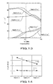
- FIG. 13 is a graph illustrating the relationship between the frequency and the magnetic permeability.
- ⁇ " represents the energy loss.
- the resonance frequency of the antenna coil 21 is 13.56MHz as described above. Then, ⁇ ' and ⁇ " of Samples A through C are as follows.
- FIG. 14 is a graph illustrating the resistances (R) and the inductances (L) of Samples A through C.
- line 111 indicates the inductances (L) while line 112 indicates the losses/resistances (R).
- R losses/resistances
- FIG. 15 is a graph illustrating the relationship between the Q values of Samples A through C and the communication distances.
- line 113 indicates the Q values of Samples A through C
- line 114 indicates the communication distances of Samples A through C.
- the Q values rises in the order of Sample A, Sample B and Sample C.
- the loss/resistance (R) and the Q value show a relationship that the Q value rises as the resistance (R) falls. Therefore, the communication distances increase in the order of Sample A, Sample B and Sample C.
- the RFID section 2c arranged at the rear side of one of the main surface of the equipment main body 2 of the above described portable telephone set 1 may additionally be provided with a reader/writer circuit.
- the substrate 42 is replaced by substrate 51 on which a first antenna coil 52 that replaces the antenna coil 21 of the RFID section 2c and a second antenna coil 53 that replaces the antenna coil 32 of the reader/writer circuit 31 are arranged.
- the first antenna coil 52 for the card is arranged in the outer circumferential side and the second antenna coil 53 for the reader/writer circuit is arranged in the inside.
- the first antenna coil 52 and the second antenna coil 53 are arranged close to each other on the same surface to downsize the antenna module.
- a non-contact type IC card circuit 54 is arranged on the first antenna coil 52 and a reader/writer circuit 55 is connected to the second antenna coil 53 in the RFID section 2c. Since the non-contact type IC card circuit 54 has a circuit configuration similar to the one illustrated in FIG. 3, it will not be described here any further. Similarly, since the reader/writer circuit 55 has a circuit configuration similar to that of the reader/writer circuit 31 shown in FIG. 4, it will not be described here any further either.
- a filter circuit 56 is arranged between the reader/writer circuit 55 and the second antenna coil 53.
- the filter circuit 56 is driven by the reader/writer circuit 55 and suppresses the signal emitted from the second antenna coil 54 to a predetermined signal level.
- the filter circuit 56 includes low pass filters and band pass filters that are inserted therein, if necessary, in order to secure the communication quality of the portable telephone set 1 and reduce any spurious emission of transmission wave, or so-called unnecessary radiation, to make the portable telephone set 1 conform to the Radio laws of different nations.
- the filter circuit 56 has a pair of low pass filters on the respective transmission lines between the reader/writer circuit 55 and the second antenna coil 53.
- the low pass filters are so called T-type tertiary low pass filters, each of which comprises a pair of coils 56a, 56b and a capacitor 56c.
- a low pass filter is inserted in one of the transmission lines and configured in such a way that one of the coils, or the coil 56a, is connected at an end thereof to an end of the second antenna coil 53 and at the other end thereof to an end of the other coil 56b while the other end of the other coil 56b is connected to connection terminal S3 and the capacitor 56c is connected at an end thereof between the pair of coils 56a, 56b and at the other end to the ground.
- another low pass filter is inserted on the other transmission line and configured in such a way that one of the coils, or the coil 56a, is connected at an end thereof to an end of the second antenna coil 53 and at the other end thereof to an end of the other coil 56b while the other end of the other coil 56b is connected to connection terminal S4 and the capacitor 56c is connected at an end thereof between the pair of coils 56a, 56b and at the other end to the ground.
- the filter circuit 56 is provided with a changeover switch 56d adapted to suppress the operation of the filter circuit 56 when the non-contact type IC card circuit 54 communicates with an external reader/writer and formed by using a MOS (complementary metal oxide semiconductor) type FET (field effect transistor).
- the changeover switch 56d has its gate connected to an output terminal S5 of changeover control circuit 57, which will be described in greater detail hereinafter, its drain connected to the other end of the capacitor 56c and its source connected to a grounding point.
- the changeover control circuit 57 turns on and off the changeover switch 56d, which is inserted in the filter circuit 56, according to the control signal supplied from the system controller 17 to the RFID section 2c. More specifically, the changeover control circuit 57 turns off the changeover switch 56d when the non-contact type IC card circuit 54 is driven for use, whereas it turns on the changeover switch 56d when the reader/writer circuit 55 is driven for use.
- the first antenna coil 52 receives the electromagnetic wave transmitted from the external reader/writer and the non-contact type IC card circuit 54 is driven to operate by the power induced by the first antenna coil 52.
- power is induced by the electromagnetic wave transmitted from the external reader/writer both in the first antenna coil 52 of the non-contact type IC card circuit 54 and the second antenna coil 53 of the reader/writer circuit 55. Therefore, the electric current I that is inducted in the second antenna coil 53 flows through the coil 31 and the capacitor 56c of the filter circuit 56 but blocked by the changeover switch 56d that is turned off.
- the changeover switch 56d that is inserted in the filter circuit 56 is turned off to raise the impedance of the capacitor 56c infinitely and consequently increase the overall impedance as viewed from the first antenna coil 52 so as to make the filter circuit 56 not constitute any load.
- the non-contact type IC card circuit 54 of the portable type telephone set 1 communicates with the external reader/writer and becomes driven to operate, the electric power induced in the second antenna coil 53 by the electromagnetic wave transmitted from the external reader/writer is prevented from flowing to the ground by way of the coil 56a and the capacitor 56c of the filter circuit 56.
- the electric power inducted in the second antenna coil 53 is not consumed and substantially all the electric power inducted by the electromagnetic wave transmitted from the external reader/writer can be used in the non-contact type IC card circuit 54.
- the changeover switch 56d inserted in the filter circuit 56 is turned on. Then, it is possible to secure the performance of the filter circuit 56 by selecting a device whose switch-on resistance is sufficiently small. Since the changeover switch 56d is not inserted directly in the signal line, it is possible to prevent the waveform passing through the changeover switch 56d from degrading and a loss of electric power from arising.
- the advantages of embodiments of the present invention are secured due to the provision of the magnetic plate 43 and the metal plate 44 arranged under the substrate 51 even when the RFID section 2c is provided with a non-contact type IC card circuit 54 and a reader/writer circuit 55 and the first antenna coil 52 and the second antenna coil 53 are arranged close to each other on the substrate 51.
- the position of the RFID section 2c is not particularly restricted so long as the antenna coil is or antenna coils are located on the inner surface side of the cabinet.
- the advantages of embodiments of the present invention are secured even when the RFID section 2c is arranged on a printed circuit board.
- embodiments of the present invention are by no means limited to portable type telephone sets so long as it is a portable type device.
- embodiments of the present invention can be applied to PDAs and portable type recording and/or reproduction devices that are adapted to use a disc cartridge or an IC card as recording medium.
- a portable type information processing terminal device comprises a substrate carrying a substantially annular antenna coil thereon, a signal processing integrated circuit element arranged inside the antenna coil, a magnetic plate arranged under the substrate and a metal plate arranged under the magnetic plate, which are integrally formed and arranged on one or more than one metal parts including a battery pack.
- the metal plate is used to roughly regulate the resonance frequency of the antenna coil so that it is allowed to be arranged in a cabinet of the portable device.
Landscapes
- Engineering & Computer Science (AREA)
- Physics & Mathematics (AREA)
- Health & Medical Sciences (AREA)
- Toxicology (AREA)
- General Physics & Mathematics (AREA)
- Theoretical Computer Science (AREA)
- Artificial Intelligence (AREA)
- Computer Vision & Pattern Recognition (AREA)
- Electromagnetism (AREA)
- Computer Networks & Wireless Communication (AREA)
- General Health & Medical Sciences (AREA)
- Architecture (AREA)
- Structural Engineering (AREA)
- Civil Engineering (AREA)
- Near-Field Transmission Systems (AREA)
- Support Of Aerials (AREA)
- Details Of Aerials (AREA)
- Telephone Function (AREA)
- Credit Cards Or The Like (AREA)
- Telephone Set Structure (AREA)
- Structure Of Receivers (AREA)
Applications Claiming Priority (2)
| Application Number | Priority Date | Filing Date | Title |
|---|---|---|---|
| JP2004024431 | 2004-01-30 | ||
| JP2004024431A JP4042702B2 (ja) | 2004-01-30 | 2004-01-30 | 携帯型情報処理端末装置 |
Publications (3)
| Publication Number | Publication Date |
|---|---|
| EP1560149A2 true EP1560149A2 (fr) | 2005-08-03 |
| EP1560149A3 EP1560149A3 (fr) | 2009-07-08 |
| EP1560149B1 EP1560149B1 (fr) | 2017-03-08 |
Family
ID=34650862
Family Applications (1)
| Application Number | Title | Priority Date | Filing Date |
|---|---|---|---|
| EP05250483.4A Expired - Lifetime EP1560149B1 (fr) | 2004-01-30 | 2005-01-28 | Terminal portable de traitement d'informations |
Country Status (5)
| Country | Link |
|---|---|
| US (1) | US7261240B2 (fr) |
| EP (1) | EP1560149B1 (fr) |
| JP (1) | JP4042702B2 (fr) |
| KR (1) | KR101064445B1 (fr) |
| CN (1) | CN100571291C (fr) |
Cited By (11)
| Publication number | Priority date | Publication date | Assignee | Title |
|---|---|---|---|---|
| FR2897179A1 (fr) * | 2006-02-07 | 2007-08-10 | Schneider Electric Ind Sas | Station de lecture/ecriture d'etiquettes electroniques |
| EP1884881A1 (fr) * | 2006-07-14 | 2008-02-06 | Sony Ericsson Mobile Communications Japan, Inc. | Circuit de communication sans contact et terminal portable |
| CN101281614B (zh) * | 2008-04-14 | 2010-06-09 | 北京大学深圳研究生院 | 一种用于超高频射频识别芯片的解调电路 |
| EP2128788A3 (fr) * | 2008-05-27 | 2011-06-29 | Brother Kogyo Kabushiki Kaisha | Appareil de communication d'étiquette RFID |
| EP2088538A4 (fr) * | 2006-10-25 | 2011-11-09 | Nec Corp | Dispositif de communication et terminal de communication portatif utilisant ce dispositif |
| US20120206307A1 (en) * | 2009-07-28 | 2012-08-16 | Sony Chemical & Information Device Corporation | Antenna device and communication device |
| EP2169839A3 (fr) * | 2008-09-29 | 2012-10-10 | TDK Corporation | Transmetteur radio |
| EP2461425A4 (fr) * | 2009-07-28 | 2013-01-16 | Sony Chem & Inf Device Corp | Dispositif d'antenne et dispositif de communication |
| EP2461424A4 (fr) * | 2009-07-28 | 2013-01-23 | Sony Chem & Inf Device Corp | Procédé de fabrication d'un dispositif d'antenne |
| US8752277B2 (en) | 2009-07-28 | 2014-06-17 | Dexerials Corporation | Method for producing antenna device |
| EP1758049B2 (fr) † | 2005-08-23 | 2018-02-21 | Inside Secure | Lecteur à couplage inductif comprenant des moyens d'extraction d'une tension d'alimentation électrique |
Families Citing this family (47)
| Publication number | Priority date | Publication date | Assignee | Title |
|---|---|---|---|---|
| JP3791923B2 (ja) * | 2004-01-13 | 2006-06-28 | 株式会社東芝 | 無線通信端末 |
| JPWO2006059487A1 (ja) * | 2004-11-30 | 2008-06-05 | 松下電器産業株式会社 | 携帯端末 |
| WO2007099592A1 (fr) * | 2006-02-28 | 2007-09-07 | Matsushita Electric Industrial Co., Ltd. | Dispositif d'antenne et dispositif electronique sur lequel est monte le dispositif d'antenne |
| JP5029605B2 (ja) | 2006-04-03 | 2012-09-19 | パナソニック株式会社 | アンテナ内蔵半導体メモリモジュール |
| JP4722774B2 (ja) * | 2006-06-19 | 2011-07-13 | 京セラ株式会社 | 電子機器 |
| US8693720B2 (en) | 2006-08-31 | 2014-04-08 | Red Tail Hawk Corporation | Wireless earplug with improved sensitivity and form factor |
| US8688036B2 (en) | 2006-08-31 | 2014-04-01 | Red Tail Hawk Corporation | Wireless communications headset system employing a loop transmitter that fits around the pinna |
| JP4915323B2 (ja) * | 2006-11-28 | 2012-04-11 | ブラザー工業株式会社 | 無線タグ情報通信装置 |
| KR100836536B1 (ko) * | 2006-12-21 | 2008-06-10 | 한국과학기술원 | 컨덕터의 안테나에 대한 영향이 감소된 에스아이피 및 그설계 방법 |
| US8061620B2 (en) | 2007-07-27 | 2011-11-22 | Mastercard International, Inc. | Removably securing small contactless payment card to electronic device |
| JP4910967B2 (ja) * | 2007-10-03 | 2012-04-04 | ソニー株式会社 | 非接触通信装置用アンテナ基板および非接触通信装置 |
| US20090159705A1 (en) * | 2007-12-24 | 2009-06-25 | Dynamics Inc. | Payment cards and devices operable to receive point-of-sale actions before point-of-sale and forward actions at point-of-sale |
| US20090212913A1 (en) * | 2008-02-21 | 2009-08-27 | Holland1916 Inc | Radio Frequency Identification Enabled Tag And Method For Its Production |
| JP4949333B2 (ja) * | 2008-07-22 | 2012-06-06 | 日本電信電話株式会社 | 読み書き装置および携帯機器 |
| US20100026458A1 (en) * | 2008-07-29 | 2010-02-04 | Disney Enterprises, Inc. | Expansion module for portable gaming devices and system for providing localized environmental interaction |
| JP2010062734A (ja) * | 2008-09-02 | 2010-03-18 | Toshiba Corp | 無線装置、アンテナ装置及び無線システム |
| JP4843658B2 (ja) * | 2008-10-09 | 2011-12-21 | フェリカネットワークス株式会社 | バッテリパック及び情報処理装置 |
| TWM368981U (en) * | 2009-07-28 | 2009-11-11 | Inventec Appliances Corp | Electronic device for wireless transmitting |
| TW201108104A (en) * | 2009-08-31 | 2011-03-01 | Walton Advanced Eng Inc | Integrated circuit module with display device |
| JP2011066627A (ja) * | 2009-09-16 | 2011-03-31 | Smart:Kk | Nfcセンサアンテナ |
| CN102035069A (zh) * | 2009-09-30 | 2011-04-27 | 深圳富泰宏精密工业有限公司 | 便携式电子装置 |
| JP2011138403A (ja) | 2009-12-28 | 2011-07-14 | Sony Corp | 情報処理装置 |
| JP2011176604A (ja) * | 2010-02-24 | 2011-09-08 | Fujitsu Toshiba Mobile Communications Ltd | 携帯端末 |
| JP5162648B2 (ja) * | 2010-12-01 | 2013-03-13 | デクセリアルズ株式会社 | アンテナ装置、及び、通信装置 |
| US8917160B2 (en) * | 2011-03-21 | 2014-12-23 | Sony Corporation | RFID module |
| US8905317B1 (en) * | 2012-06-07 | 2014-12-09 | Amazon Technologies, Inc. | Co-located passive UHF RFID tag and NFC antenna in compact electronic devices |
| JP6033603B2 (ja) * | 2012-08-08 | 2016-11-30 | シャープ株式会社 | 携帯端末 |
| US9083388B2 (en) * | 2012-08-29 | 2015-07-14 | Red Tail Hawk Corporation | Transmitter with improved sensitivity and shielding |
| CN104756317B (zh) * | 2012-10-26 | 2017-09-26 | 株式会社村田制作所 | 接口、通信装置以及程序 |
| US9620843B2 (en) * | 2013-01-31 | 2017-04-11 | Hewlett-Packard Development Company, L.P. | Display panel for front-side wireless communication |
| USD710231S1 (en) | 2013-02-18 | 2014-08-05 | Holland 1916, Inc. | Housing for electronic tag |
| JP6112923B2 (ja) * | 2013-03-14 | 2017-04-12 | Necトーキン株式会社 | アンテナ、アンテナ構造体及び電子機器 |
| KR20140115209A (ko) * | 2013-03-20 | 2014-09-30 | 삼성에스디아이 주식회사 | 안테나를 갖는 배터리 팩 |
| WO2014156285A1 (fr) * | 2013-03-25 | 2014-10-02 | 株式会社村田製作所 | Dispositif d'antenne et dispositif de communication |
| KR101467706B1 (ko) * | 2013-11-21 | 2014-12-01 | 광운대학교 산학협력단 | 루프 간에 상쇄 전류가 감소된 성능이 개선된 nfc 안테나 구조 |
| WO2015115401A1 (fr) * | 2014-01-30 | 2015-08-06 | 株式会社村田製作所 | Appareil de communication sans fil |
| KR101762778B1 (ko) | 2014-03-04 | 2017-07-28 | 엘지이노텍 주식회사 | 무선 충전 및 통신 기판 그리고 무선 충전 및 통신 장치 |
| KR102110886B1 (ko) * | 2014-04-24 | 2020-05-14 | 삼성전자주식회사 | 기판 탑재형 방사체를 구비한 휴대용 전자 장치 |
| KR101681409B1 (ko) * | 2015-04-16 | 2016-12-12 | 삼성전기주식회사 | 코일 전자부품 |
| JP2017085418A (ja) * | 2015-10-29 | 2017-05-18 | キヤノン株式会社 | 電子機器 |
| USD821401S1 (en) * | 2016-01-29 | 2018-06-26 | Siebels Asset Management Research, Ltd. | Controlled document tracking and/or authentication device |
| JPWO2018003792A1 (ja) * | 2016-06-27 | 2019-04-11 | 日本電産サンキョー株式会社 | カードリーダ |
| US10249456B2 (en) | 2017-03-21 | 2019-04-02 | Illinois Tool Works Inc. | Apparatus with membrane panel having close-proximity communication antenna |
| JP6987579B2 (ja) * | 2017-09-21 | 2022-01-05 | ラピスセミコンダクタ株式会社 | 電池ユニット、電池監視システム、電池交換方法 |
| KR102453075B1 (ko) * | 2018-03-09 | 2022-10-11 | 도레이 카부시키가이샤 | 무선 통신 장치 |
| CN111092286B (zh) * | 2019-12-05 | 2022-10-14 | 航天信息股份有限公司 | 便携式rfid读写器用天线及其使用结合方法 |
| CN112749571B (zh) * | 2020-12-28 | 2022-07-05 | 杭州海康威视数字技术股份有限公司 | 读卡终端及无线射频识别系统 |
Citations (1)
| Publication number | Priority date | Publication date | Assignee | Title |
|---|---|---|---|---|
| EP1347533A1 (fr) | 2000-12-18 | 2003-09-24 | Mitsubishi Materials Corporation | Antenne rfid |
Family Cites Families (28)
| Publication number | Priority date | Publication date | Assignee | Title |
|---|---|---|---|---|
| US5642120A (en) * | 1993-03-29 | 1997-06-24 | Seiko Epson Corporation | Antenna device and wireless apparatus employing the same |
| JPH06344692A (ja) | 1993-06-04 | 1994-12-20 | Toshiba Corp | 薄型モジュール |
| JP3085507B2 (ja) | 1994-03-25 | 2000-09-11 | ホーチキ株式会社 | アンテナ装置 |
| JP3255221B2 (ja) | 1996-11-29 | 2002-02-12 | 三菱マテリアル株式会社 | 盗難防止用タグ |
| EP0886232B1 (fr) * | 1997-06-20 | 2007-09-05 | Hitachi, Ltd. | Lecteur-enregistreur, système d'alimentation et système de communication |
| JPH11250205A (ja) | 1998-02-27 | 1999-09-17 | Tokin Corp | Icカード |
| JPH11250207A (ja) | 1998-03-03 | 1999-09-17 | Nagase & Co Ltd | Icモジュール、その製造方法及び該モジュールを搭載した非接触型icカード |
| JP4340929B2 (ja) * | 1998-10-02 | 2009-10-07 | ソニー株式会社 | メモリicタグ装置 |
| JP2000163544A (ja) * | 1998-12-01 | 2000-06-16 | Rohm Co Ltd | 半導体装置 |
| JP3838815B2 (ja) * | 1999-05-10 | 2006-10-25 | 日本電気株式会社 | 携帯電話機 |
| JP2001006007A (ja) | 1999-06-23 | 2001-01-12 | Casio Comput Co Ltd | データ通信装置及びデータ通信システム |
| JP2001024425A (ja) | 1999-07-06 | 2001-01-26 | Kitagawa Ind Co Ltd | ループアンテナ用積層体 |
| JP2001044747A (ja) | 1999-07-27 | 2001-02-16 | Nec Corp | 非接触型icカードのリードライト装置 |
| JP2001307051A (ja) | 2000-04-21 | 2001-11-02 | Sony Corp | アンテナ付き回路基板およびアンテナ付き回路基板の製造方法および容量付き回路基板および容量付き回路基板の製造方法およびアンテナ及び容量付き回路基板およびアンテナ及び容量付き回路基板の製造方法および非接触型情報授受装置 |
| JP2001307032A (ja) | 2000-04-27 | 2001-11-02 | Matsushita Electric Ind Co Ltd | 携帯端末 |
| JP2001319192A (ja) | 2000-05-12 | 2001-11-16 | Matsushita Electric Ind Co Ltd | カードリーダ |
| JP3776310B2 (ja) | 2000-12-15 | 2006-05-17 | ボーダフォン株式会社 | Icカード |
| JP3642029B2 (ja) * | 2001-02-06 | 2005-04-27 | 日本電気株式会社 | 携帯電話機 |
| JP2002279383A (ja) | 2001-03-22 | 2002-09-27 | Toppan Printing Co Ltd | 非接触型ic記録媒体用アンテナの形成方法、この形成方法に使用するシート及び非接触型ic記録媒体 |
| JP4578728B2 (ja) | 2001-07-02 | 2010-11-10 | 株式会社ハネックス | 携帯型機器 |
| JP4670195B2 (ja) | 2001-07-23 | 2011-04-13 | 凸版印刷株式会社 | 非接触式icカードを備えた携帯電話機用筐体 |
| JP2003046627A (ja) | 2001-07-27 | 2003-02-14 | Dainippon Printing Co Ltd | Icタグ付き携帯電話機 |
| JP2003087385A (ja) | 2001-09-14 | 2003-03-20 | Mbr:Kk | 携帯情報端末 |
| JP2003099733A (ja) | 2001-09-25 | 2003-04-04 | Nec Tokin Corp | Icカードリーダライタのアンテナユニット |
| JP2003216899A (ja) | 2002-01-22 | 2003-07-31 | Hitachi Cable Ltd | 携帯型無線端末及びそれを用いた情報移転システム |
| CN1659588A (zh) | 2002-06-10 | 2005-08-24 | 坂村健 | Ic芯片和与其连接的卡以及移动终端装置 |
| JP2005026743A (ja) * | 2003-06-30 | 2005-01-27 | Matsushita Electric Ind Co Ltd | アンテナ一体型非接触icカード読取/書込装置 |
| JP2005033413A (ja) * | 2003-07-10 | 2005-02-03 | Matsushita Electric Ind Co Ltd | ループアンテナ及び非接触icカード読取/書込装置 |
-
2004
- 2004-01-30 JP JP2004024431A patent/JP4042702B2/ja not_active Expired - Fee Related
-
2005
- 2005-01-25 US US11/042,786 patent/US7261240B2/en not_active Expired - Lifetime
- 2005-01-28 KR KR1020050007869A patent/KR101064445B1/ko not_active Expired - Fee Related
- 2005-01-28 EP EP05250483.4A patent/EP1560149B1/fr not_active Expired - Lifetime
- 2005-01-31 CN CNB2005100062009A patent/CN100571291C/zh not_active Expired - Fee Related
Patent Citations (1)
| Publication number | Priority date | Publication date | Assignee | Title |
|---|---|---|---|---|
| EP1347533A1 (fr) | 2000-12-18 | 2003-09-24 | Mitsubishi Materials Corporation | Antenne rfid |
Cited By (16)
| Publication number | Priority date | Publication date | Assignee | Title |
|---|---|---|---|---|
| EP1758049B2 (fr) † | 2005-08-23 | 2018-02-21 | Inside Secure | Lecteur à couplage inductif comprenant des moyens d'extraction d'une tension d'alimentation électrique |
| US8269611B2 (en) | 2006-02-07 | 2012-09-18 | Schneider Electric Industries Sas | Electronic tag reading/writing station |
| FR2897179A1 (fr) * | 2006-02-07 | 2007-08-10 | Schneider Electric Ind Sas | Station de lecture/ecriture d'etiquettes electroniques |
| EP1884881A1 (fr) * | 2006-07-14 | 2008-02-06 | Sony Ericsson Mobile Communications Japan, Inc. | Circuit de communication sans contact et terminal portable |
| US7907056B2 (en) | 2006-07-14 | 2011-03-15 | Sony Ericsson Mobile Communications Japan, Inc. | Contactless communication circuit and portable terminal |
| EP2088538A4 (fr) * | 2006-10-25 | 2011-11-09 | Nec Corp | Dispositif de communication et terminal de communication portatif utilisant ce dispositif |
| EP2793174A1 (fr) * | 2006-10-25 | 2014-10-22 | NEC Corporation | Dispositif de communication et terminal de communication portable l'utilisant |
| CN101281614B (zh) * | 2008-04-14 | 2010-06-09 | 北京大学深圳研究生院 | 一种用于超高频射频识别芯片的解调电路 |
| EP2128788A3 (fr) * | 2008-05-27 | 2011-06-29 | Brother Kogyo Kabushiki Kaisha | Appareil de communication d'étiquette RFID |
| US8242913B2 (en) | 2008-05-27 | 2012-08-14 | Brother Kogyo Kabushiki Kaisha | RFID tag communication apparatus |
| EP2169839A3 (fr) * | 2008-09-29 | 2012-10-10 | TDK Corporation | Transmetteur radio |
| EP2461425A4 (fr) * | 2009-07-28 | 2013-01-16 | Sony Chem & Inf Device Corp | Dispositif d'antenne et dispositif de communication |
| EP2461424A4 (fr) * | 2009-07-28 | 2013-01-23 | Sony Chem & Inf Device Corp | Procédé de fabrication d'un dispositif d'antenne |
| US8745855B2 (en) | 2009-07-28 | 2014-06-10 | Dexerials Corporation | Method for producing antenna device |
| US8752277B2 (en) | 2009-07-28 | 2014-06-17 | Dexerials Corporation | Method for producing antenna device |
| US20120206307A1 (en) * | 2009-07-28 | 2012-08-16 | Sony Chemical & Information Device Corporation | Antenna device and communication device |
Also Published As
| Publication number | Publication date |
|---|---|
| EP1560149A3 (fr) | 2009-07-08 |
| KR101064445B1 (ko) | 2011-09-14 |
| JP4042702B2 (ja) | 2008-02-06 |
| CN1649364A (zh) | 2005-08-03 |
| CN100571291C (zh) | 2009-12-16 |
| JP2005217946A (ja) | 2005-08-11 |
| EP1560149B1 (fr) | 2017-03-08 |
| KR20050078224A (ko) | 2005-08-04 |
| US20050178835A1 (en) | 2005-08-18 |
| US7261240B2 (en) | 2007-08-28 |
Similar Documents
| Publication | Publication Date | Title |
|---|---|---|
| EP1560149B1 (fr) | Terminal portable de traitement d'informations | |
| EP1477927B1 (fr) | Dispositif d antenne et dispositif de communication utilisan t un dispositif d antenne | |
| JP4466689B2 (ja) | アンテナ及び携帯電子機器 | |
| JP4232474B2 (ja) | 通信機能付き電子機器 | |
| US8406686B2 (en) | Wireless communication terminal apparatus and method of controlling same | |
| US7699231B2 (en) | Reader/writer and mobile communication apparatus | |
| US9362985B2 (en) | Portable apparatus and feed system | |
| US20070069961A1 (en) | Magnetic core member for antenna module, antenna module and portable information terminal equipped with antenna module | |
| US20080238799A1 (en) | Near field communication antenna and mobile device | |
| GB2510509A (en) | Power reception device, power transmission device, and wireless power transmission system | |
| KR20060060545A (ko) | 무선 통신 단말기, 무선 통신 단말기 수용 케이스, 무선통신 단말기 대응 시트, 및 무선 통신 단말기 대응 표시기기 | |
| JP2006005836A (ja) | 携帯情報端末 | |
| JP2005236585A (ja) | アンテナモジュール及びこれを備えた携帯情報端末 | |
| JP4264534B2 (ja) | データ通信装置、非接触データ送受信システム、及びアンテナ装置 | |
| JP4380275B2 (ja) | データ通信装置 | |
| JP2005234827A (ja) | アンテナモジュール及びこれを備えた携帯情報端末 | |
| JP2005236586A (ja) | アンテナモジュール及びこれを備えた携帯情報端末 | |
| CN101136505B (zh) | 天线及便携电子设备 | |
| CN101136505A (zh) | 天线及便携电子设备 |
Legal Events
| Date | Code | Title | Description |
|---|---|---|---|
| PUAI | Public reference made under article 153(3) epc to a published international application that has entered the european phase |
Free format text: ORIGINAL CODE: 0009012 |
|
| AK | Designated contracting states |
Kind code of ref document: A2 Designated state(s): AT BE BG CH CY CZ DE DK EE ES FI FR GB GR HU IE IS IT LI LT LU MC NL PL PT RO SE SI SK TR |
|
| AX | Request for extension of the european patent |
Extension state: AL BA HR LV MK YU |
|
| PUAL | Search report despatched |
Free format text: ORIGINAL CODE: 0009013 |
|
| AK | Designated contracting states |
Kind code of ref document: A3 Designated state(s): AT BE BG CH CY CZ DE DK EE ES FI FR GB GR HU IE IS IT LI LT LU MC NL PL PT RO SE SI SK TR |
|
| AX | Request for extension of the european patent |
Extension state: AL BA HR LV MK YU |
|
| RIC1 | Information provided on ipc code assigned before grant |
Ipc: G06K 7/00 20060101AFI20050427BHEP Ipc: G06K 19/077 20060101ALI20090604BHEP |
|
| 17P | Request for examination filed |
Effective date: 20090714 |
|
| 17Q | First examination report despatched |
Effective date: 20090819 |
|
| AKX | Designation fees paid |
Designated state(s): DE FR GB |
|
| GRAP | Despatch of communication of intention to grant a patent |
Free format text: ORIGINAL CODE: EPIDOSNIGR1 |
|
| INTG | Intention to grant announced |
Effective date: 20160902 |
|
| STAA | Information on the status of an ep patent application or granted ep patent |
Free format text: STATUS: GRANT OF PATENT IS INTENDED |
|
| GRAS | Grant fee paid |
Free format text: ORIGINAL CODE: EPIDOSNIGR3 |
|
| GRAA | (expected) grant |
Free format text: ORIGINAL CODE: 0009210 |
|
| STAA | Information on the status of an ep patent application or granted ep patent |
Free format text: STATUS: THE PATENT HAS BEEN GRANTED |
|
| AK | Designated contracting states |
Kind code of ref document: B1 Designated state(s): DE FR GB |
|
| REG | Reference to a national code |
Ref country code: GB Ref legal event code: FG4D |
|
| REG | Reference to a national code |
Ref country code: DE Ref legal event code: R096 Ref document number: 602005051456 Country of ref document: DE |
|
| REG | Reference to a national code |
Ref country code: DE Ref legal event code: R097 Ref document number: 602005051456 Country of ref document: DE |
|
| PLBE | No opposition filed within time limit |
Free format text: ORIGINAL CODE: 0009261 |
|
| STAA | Information on the status of an ep patent application or granted ep patent |
Free format text: STATUS: NO OPPOSITION FILED WITHIN TIME LIMIT |
|
| REG | Reference to a national code |
Ref country code: FR Ref legal event code: PLFP Year of fee payment: 14 |
|
| 26N | No opposition filed |
Effective date: 20171211 |
|
| REG | Reference to a national code |
Ref country code: GB Ref legal event code: 746 Effective date: 20211108 |
|
| PGFP | Annual fee paid to national office [announced via postgrant information from national office to epo] |
Ref country code: FR Payment date: 20211215 Year of fee payment: 18 Ref country code: GB Payment date: 20211216 Year of fee payment: 18 |
|
| PGFP | Annual fee paid to national office [announced via postgrant information from national office to epo] |
Ref country code: DE Payment date: 20211215 Year of fee payment: 18 |
|
| REG | Reference to a national code |
Ref country code: DE Ref legal event code: R119 Ref document number: 602005051456 Country of ref document: DE |
|
| GBPC | Gb: european patent ceased through non-payment of renewal fee |
Effective date: 20230128 |
|
| PG25 | Lapsed in a contracting state [announced via postgrant information from national office to epo] |
Ref country code: GB Free format text: LAPSE BECAUSE OF NON-PAYMENT OF DUE FEES Effective date: 20230128 Ref country code: DE Free format text: LAPSE BECAUSE OF NON-PAYMENT OF DUE FEES Effective date: 20230801 |
|
| PG25 | Lapsed in a contracting state [announced via postgrant information from national office to epo] |
Ref country code: FR Free format text: LAPSE BECAUSE OF NON-PAYMENT OF DUE FEES Effective date: 20230131 |