EP1560276A2 - Dispositif émettant de lumière fabriqué de matériau III-nitrure ayant des champs de polarisation réduits - Google Patents
Dispositif émettant de lumière fabriqué de matériau III-nitrure ayant des champs de polarisation réduits Download PDFInfo
- Publication number
- EP1560276A2 EP1560276A2 EP05100413A EP05100413A EP1560276A2 EP 1560276 A2 EP1560276 A2 EP 1560276A2 EP 05100413 A EP05100413 A EP 05100413A EP 05100413 A EP05100413 A EP 05100413A EP 1560276 A2 EP1560276 A2 EP 1560276A2
- Authority
- EP
- European Patent Office
- Prior art keywords
- layer
- net polarization
- spacer
- light emitting
- spacer layers
- Prior art date
- Legal status (The legal status is an assumption and is not a legal conclusion. Google has not performed a legal analysis and makes no representation as to the accuracy of the status listed.)
- Granted
Links
Images


Classifications
-
- H—ELECTRICITY
- H10—SEMICONDUCTOR DEVICES; ELECTRIC SOLID-STATE DEVICES NOT OTHERWISE PROVIDED FOR
- H10H—INORGANIC LIGHT-EMITTING SEMICONDUCTOR DEVICES HAVING POTENTIAL BARRIERS
- H10H20/00—Individual inorganic light-emitting semiconductor devices having potential barriers, e.g. light-emitting diodes [LED]
- H10H20/80—Constructional details
- H10H20/81—Bodies
- H10H20/822—Materials of the light-emitting regions
- H10H20/824—Materials of the light-emitting regions comprising only Group III-V materials, e.g. GaP
- H10H20/825—Materials of the light-emitting regions comprising only Group III-V materials, e.g. GaP containing nitrogen, e.g. GaN
Definitions
- the present invention relates to III-nitride light emitting devices.
- LEDs light emitting diodes
- RCLEDs resonant cavity light emitting diodes
- VCSELs vertical cavity laser diodes
- edge emitting lasers are among the most efficient light sources currently available.
- Materials systems currently of interest in the manufacture of high-brightness light emitting devices capable of operation across the visible spectrum include Group III-V semiconductors, particularly binary, ternary, and quaternary alloys of gallium, aluminum, indium, and nitrogen, also referred to as III-nitride materials.
- III-nitride light emitting devices are fabricated by epitaxially growing a stack of semiconductor layers of different compositions and dopant concentrations on a sapphire, silicon carbide, III-nitride, or other suitable substrate by metal-organic chemical vapor deposition (MOCVD), molecular beam epitaxy (MBE), or other epitaxial techniques.
- MOCVD metal-organic chemical vapor deposition
- MBE molecular beam epitaxy
- the stack often includes one or more n-type layers doped with, for example, Si, formed over the substrate, a light emitting or active region formed over the n-type layer or layers, and one or more p-type layers doped with, for example, Mg, formed over the active region.
- III-nitride devices formed on conductive substrates may have the p- and n-contacts formed on opposite sides of the device.
- III-nitride devices are fabricated on insulating substrates, such as sapphire, with both contacts on the same side of the device. Such devices are mounted so light is extracted either through the contacts (known as an epitaxy-up device) or through a surface of the device opposite the contacts (known as a flip chip device).
- the crystal layers in III-nitride devices are often grown as strained wurtzite crystals on lattice-mismatched substrates such as sapphire.
- Such crystals exhibit two types of polarization, spontaneous polarization, which arises from the difference of alloy composition between layers of different composition, and piezoelectric polarization, which arises due to the strain in the layers of the device.
- the total polarization in a layer is the sum of the spontaneous and piezoelectric polarization.
- Fig. 1A is a sectional view schematically illustrating a typical conventional strained wurtzite nitride double heterostructure semiconductor, described in U.S. Patent 6,515,313.
- the illustrated substrate layer 1 may be any material suitable for growing nitride semiconductors, including spinel (MgAl 2 O 4 ), sapphire (Al 2 O 3 ), SiC (including 6H, 4H, and 3C), ZnS, ZnO, GaAs, AlN and GaN.
- the substrate thickness typically ranges from 100 ⁇ m to 1 mm.
- a buffer layer 2 on the substrate 1 can be formed of AlN, GaN, AlGaN, InGaN or the like.
- the buffer layer facilitates possible lattice mismatches between the substrate 1 and an overlying conductive contact layer 3.
- the buffer layer 2 may be omitted if the substrate has a lattice constant approximately equal to that of the nitride semiconductor.
- the buffer layer 2 may also be omitted with some nitride growth techniques.
- the buffer layer energy bandgap may range from 2.1 eV to 6.2 eV, with a thickness of about 0.5 ⁇ m to 10 ⁇ m.
- the n-type contact layer 3 is also typically formed from a nitride semiconductor, preferably GaN or InGaN with a thickness ranging from 0.5 ⁇ m to 5.0 ⁇ m, and a bandgap of approximately 3.4 eV for GaN and less for InGaN (depending upon the Indium concentration).
- a lower n-type or undoped cladding layer 4 on the conductive layer 3 conventionally comprises GaN or AlGaN, with a bandgap of 3.4 eV for GaN and greater for AlGaN (depending upon the Al concentration). Its thickness can range from 1 nm to 100 nm.
- Nitride double heterostructures typically employ InGaN as an active region 5 over the lower cladding layer, with a thickness of 1 nm to 100 nm.
- the bandgap of this layer is typically 2.8 eV for blue emission, but may vary depending upon the Indium concentration.
- a top p-type or undoped cladding layer 6 over the active region is generally comprised of AlGaN or GaN, with a thickness and bandgap energy similar to that of the lower n-type cladding layer 4.
- a p-type GaN conductive contact layer 7 on the cladding layer 6 has an energy bandgap of about 3.4 eV and a thickness of about 10 nm to 500 nm.
- a polarization-induced sheet charge occurs at the interface between layers due to different constituent materials. Of particular concern for the operation of a light emitter are the polarization-induced sheet charges adjacent to the active region 5.
- a negative polarization-induced sheet charge density ⁇ 1 with a magnitude such as 10 13 electrons/cm 2 , is typically formed at the interface between the active region 5 and the lower cladding layer 4.
- a positive sheet charge density ⁇ 2 of similar magnitude is formed at the interface between the active region 5 and the upper cladding layer 6.
- the polarities of these charges depend upon the bonds of the crystal layers. In general, the density of a sheet charge will depend upon both a spontaneous factor arising from compositional differences between the two layers, and a piezoelectric strain arising from the lattice mismatch between the layers.
- ⁇ 1 between an In 0.2 Ga 0.8 N active region 5 and a GaN cladding layer 4 is about 8.3 x 10 12 electrons/cm 2 . This is due to the 20% Indium content in the In 0.2 Ga 0.8 N active region (spontaneous polarization), and the strain in that layer arising from the lattice mismatch with the underlying GaN layer (piezoelectric polarization).
- Fig. 1B illustrates the energy bands corresponding to the device structure of Fig. 1A.
- the naturally occurring polarization field generated by ⁇ 1 and ⁇ 2 reduces the efficiency in a number of ways.
- the dipole leads to a spatial separation (movement in the opposite direction) of electrons and holes within the region.
- holes in the valence band E v are attracted to the negative sheet charge ⁇ 1 at one end of the active region 5, while electrons in the conduction band E c are attracted to the positive sheet charge ⁇ 2 at its other end.
- This spatial separation of free carriers lowers the probability of radiative recombination, reducing emission efficiency.
- the energy barriers of the conduction and valence band quantum wells are reduced by quantization effects associated with the electric field.
- carriers below E v and above E c escape the well through the paths indicated by dashed lines A.
- the presence of polarization-induced fields also leads to carrier overshoots, illustrated by carrier trajectories B, from the higher E c level on the ⁇ 1 side of the active region to the lower E c level on the ⁇ 2 side, and from the lower E v level on the ⁇ 2 side of the active region to the higher E v level on the ⁇ 1 side.
- a semiconductor light emitting device includes a light emitting layer sandwiched between two spacer layers.
- the difference between the net polarization in at least one of the spacer layers and the net polarization in the light emitting layer is less than in the device with conventional spacer layers, such as GaN spacer layers.
- the difference between the net polarization in at least one of the spacer layers and the net polarization in the light emitting layer is less than about 0.02 C/m 2 .
- at least one of the spacer layers is a quaternary alloy of aluminum, indium, gallium, and nitrogen.
- Matching the net polarization in the spacer layers and the light emitting layers may move polarization-induced sheet charges away from the interfaces between the spacer layers and the light emitting layer to the interface between the p- and n-type regions and the spacer layers.
- the interface between the p- and n-type regions and the spacer layers is doped, which may reduce the polarization field across the light emitting layer. Accordingly, matching the net polarization in the spacer layers and the light emitting layers, and canceling sheet charges by doping may avoid the inefficiencies caused by polarization, described above.
- Fig. 2 illustrates a device according to several embodiments of the invention.
- An n-type region 21 is formed over a suitable substrate 20, usually sapphire, SiC, or GaN.
- Active region 23 is sandwiched between two spacer layers, an n-type spacer layer 22 and a p-type spacer layer 24.
- Active region 23 may be a single light emitting layer or may include one or more quantum well layers separated by barrier layers.
- a p-type region 25 is formed over p-type spacer layer 24.
- P-contact 26 provides electrical contact to the p-side of the active region and n-contact 27 provides electrical contact to the n-side of the active region. Two possible arrangements of the p- and n-contacts are described below in Figs. 7-10.
- one or more of p-type spacer layer 24, n-type spacer layer 22, and the barrier layers separating the quantum wells in a multiple quantum well active region may be quaternary alloys of aluminum, indium, gallium, and nitrogen.
- the composition of aluminum, indium, and gallium in the barrier layers and/or in spacer layers 22 and 24 are selected to match the net polarization within the light emitting layers of active region 23, or to minimize the difference in net polarization between the light emitting layers of the active region and the spacer layers and/or barrier layers.
- the net polarization in each layer is the sum of the spontaneous polarization and the piezoelectric polarization.
- the quaternary compositions required in the barrier layers and/or in spacer layers is based on the composition of the active region, which, along with the structure of the active region, determines the color of light emitted by the active region.
- Quaternary layers may be grown by techniques known in the art such as atmospheric pressure growth or pulsed metalorganic chemical vapor deposition (also known as pulsed atomic layer epitaxy).
- pulsed metalorganic chemical vapor deposition also known as pulsed atomic layer epitaxy.
- pulsed metalorganic chemical vapor deposition see, for example, J. Zhang et al., "Pulsed Atomic Layer Epitaxy of Quaternary AlInGaN Layers," 79 Appl. Phys. Lett. 925 (2001) and C.
- the composition of the spacer layers are selected such that the difference in net polarization between the light emitting layers of the active region and at least one of the spacer layers is zero.
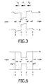
- the use of spacer layers with the same net polarization as the light emitting layers of the active region effectively cancels the sheet charges (shown in Fig. 1B) at the interface between the spacer layer and the active region.
- Fig. 3 also illustrates that the sheet charges and resulting curves in the energy band diagram are not eliminated entirely, but are shifted from the interfaces between the active region and the spacer layers to the interfaces between the spacer layers and the p- and n-type regions.
- the composition of the spacer layers is selected such that the barrier height is enough to provide a sufficient barrier, but the difference in net polarization between the light emitting layers of the active region and the spacer layers is less than in a device with conventional spacer layers, such as GaN spacer layers.
- the barrier height is defined as the difference between the band gap in the spacer layer and the band gap in the light emitting layers of the active region.
- the higher the composition of aluminum and indium in a quaternary III-nitride layer the more difficult it is to grow a layer of high crystal quality.
- spacer layers according to the first embodiment have high compositions of aluminum and indium.
- devices according to the second embodiment do not completely cancel the sheet charges at the interface between the spacer layer and the active region, these devices have potentially smaller sheet charges than devices with conventional barriers, and potentially better crystal quality spacer layers than devices according to the first embodiment. Both effects may increase the efficiency of devices according to the second embodiment.
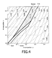
- Fig. 4 illustrates how to determine the appropriate composition of the spacer layers for the first and second embodiments, given an active region composition.
- Fig. 4 is a contour plot of the polarization and the bandgap of an Al x In y Ga z N film vs. aluminum nitride composition and indium nitride composition.
- the Al x In y Ga z N film is assumed to be coherently grown on GaN.
- the solid contour lines represent the net polarization in C/m 2 .
- the dashed contour lines represent the band gap in eV.
- Fig. 4 illustrates an example of an InGaN active layer of 10% indium, In 0.1 Ga 0.9 N (labeled "Active”), which may emit blue light when forward biased.
- 0.1 Ga 0.9 N has a band gap of about 3.1 eV and a net polarization of about 0.01 C/m 2 .
- the minimum barrier height is arbitrarily selected to be 0.2 eV. In other embodiments, the minimum barrier height may be larger or smaller, for example 0.3 eV or 0.1 eV.
- a composition range for spacer layers according to the first embodiment, where the spacer layers have the same net polarization as the active region can be determined by following the 0.01 C/m 2 contour line in the direction of increasing indium composition and increasing aluminum composition until a composition with a band gap of at least 3.3 is reached, about Al 0.20 In 0.22 Ga 0.58 N. Any spacer layer composition at this point or above along the 0.01 C/m 2 contour line (the solid line marked "First" on Fig. 4) will provide a barrier height of at least 0.2 eV with the same net polarization as the active region.
- a composition range for spacer layers according to the second embodiment, where the spacer layers have a minimum barrier height and a net polarization less than that of a conventional spacer layer is illustrated as shaded region "A" in Fig. 4.
- This region is bordered on the bottom right hand side by a curved line between about In 0.03 Ga 0.97 N and about Al 0.20 In 0.22 Ga 0.58 N, following a contour line representing the minimum barrier height of 0.2 eV.
- Region A is bordered on the top right hand side by a curved line between about Al 0.20 In 0.22 Ga 0.58 N and about Al 0.45 In 0.34 Ga 0.21 N, representing the first embodiment composition range.
- Region A is bordered on the left hand side by a curved line between about GaN and about Al 0.45 In 0.26 Ga 0.29 N, following a contour line representing the net polarization of a GaN spacer layer (labeled "GaN" on Fig. 4). Any spacer layer composition within this shaded region will have at least a 0.2 eV barrier and a net polarization less than that of a GaN spacer layer.
- the solid line within region A represents spacer layer compositions that have the same barrier height as a GaN spacer layer, but a net polarization less than that of a GaN spacer layer.
- Fig. 5 illustrates an example of an InGaN active layer of 20% indium, In 0.2 Ga 0.8 N, which may emit green light when forward biased.
- the In 0.2 Ga 0.8 N active region (labeled "Active") has a net polarization of about 0.021 C/m 2 and a band gap of about 2.9 eV.
- the minimum barrier height is again arbitrarily selected to be 0.2 eV.
- a composition range for spacer layers according to the first embodiment, where the spacer layers have the same net polarization as the active region, is determined by following the 0.021 C/m 2 contour line to the composition where the difference in band gap is at least 0.2eV, a composition of about Al 0.17 In 0.28 Ga 0.55 N, which has a band gap of 3.1 eV. Any composition at this point or above along the 0.021 C/m 2 contour line (the line labeled "First" in Fig. 5) will provide a sufficiently high barrier spacer layer with the same net polarization as the active region.
- This region is bordered on the bottom right hand side by a curved line between about In 0.12 Ga 0.88 N and about Al 0.17 In 0.28 Ga 0.55 N, following a contour line representing the minimum barrier height of 0.2 eV.
- Region B is bordered on the top right hand side by a curved line between about Al 0.17 In 0.28 Ga 0.55 N and about Al 0.45 In 0.40 Ga 0.15 N, representing the first embodiment composition range.
- Region B is bordered on the left hand side by a curved line between about GaN and about Al 0.45 In 0.26 Ga 0.29 N, following a contour line representing the net polarization of a GaN spacer layer (labeled "GaN"). Any spacer layer composition within this shaded region will have a least a 0.2 eV barrier and a net polarization less than a GaN spacer layer.
- the solid line within region B represents spacer layer compositions with the same barrier height as a GaN spacer layer, but a net polarization less than that of a GaN spacer layer.
- FIGs. 4 and 5 end at aluminum nitride and indium nitride compositions of 45%, layers with greater aluminum nitride and indium nitride compositions may be appropriate.
- the data illustrated in Figs. 4 and 5 is not meant to limit the invention.
- the data in Figs. 4 and 5 were calculated using techniques well known in the art and using the following material parameters.
- P ( P sp - P spGaN )+ P pz
- U.S. Patent 6,515,313 teaches "incorporating various dopants into the semiconductor.
- the dopant impurity should be of a type that does not diffuse away from its intended position.
- the dopants ionize, based upon their energy levels, into either positive or negative charge states, which are opposite to the interfacial polarization-induced charge states, to cancel or reduce its effect.”
- U.S. Patent 6,515,313 incorporates the dopants at the interfaces between the spacer layers and the active region. The incorporation of dopants, especially Mg, so close to the active region can degrade the crystal quality of the active region.
- the sheet charges are eliminated by making the spacer layers sufficiently thick to "screen" the active region from the sheet charges at the interfaces between the p- and n-type regions and the spacer layers, then doping the interfaces with the sheet charge with a dopant that neutralizes the sheet charge.
- the spacer layers often have a thickness between about 50 angstroms and about 200 angstroms.
- the spacer layers may have a thickness between about 500 angstroms and the critical thickness of the spacer layer, defined as the maximum thickness of the spacer layer that can be grown without cracking or relaxing.
- the thick spacer layers usually have a thickness between about 200 angstroms and about 1000 angstroms. In general, the thickness of the thick spacer layers is chosen to be thick enough to shield the active region from the doping to cancel the sheet charges, and thin enough to permit growth of a high crystal quality spacer layer.
- a negative sheet charge accumulates at the interface between n-type or undoped spacer layer 22 and n-type region 21. This sheet charge may be canceled by incorporating a region of highly n-type doped material as close to the interface as possible.
- the highly doped region may be in the part of n-type region 21 or spacer layer 22 adjacent to the interface. For example, a region 10 angstroms thick and having a Si concentration between about 1x10 18 cm -3 and 1x10 20 cm -3 may be incorporated in n-type region 21 or spacer layer 22, immediately adjacent to the interface between these two layers. More preferably, the highly doped region has a Si concentration between about 5x10 19 cm -3 and 1x10 20 cm -3 .
- a positive sheet charge accumulates at the interface between p-type spacer layer 24 and p-type region 25.
- This sheet charge may be canceled by incorporating a region of highly p-type doped material in the part of p-type region 25 or spacer layer 24 adjacent to the interface.
- a region 10 angstroms thick and having a Mg concentration between about 1x10 18 cm -3 and 1x10 20 cm -3 may be incorporated in p-type region 25 or spacer layer 24, immediately adjacent to the interface between these two layers.
- the highly doped region has a Mg concentration between about 5x10 19 cm -3 and 1x10 20 cm -3 .
- the amount of doping required at the interfaces between the spacer layers and the p- and n-type regions may depend on the magnitude of the sheet charge, which depends on the compositions of the layers in the device.
- the thickness and dopant concentration are selected such that the dopant concentration in the highly doped area times the thickness of the highly doped area is about equal to the sheet charge at the interface. Accordingly, the higher the dopant concentration in the highly doped area, the thinner this area needs to be to cancel the sheet charge.
- the sheet charges may be canceled by incorporating lower concentrations of dopants in the n- and p-type regions or in the spacer layers over greater thicknesses.
- the magnitude of the sheet change increases.
- the sheet charges in the device with 20% indium quantum wells may be twice the magnitude of the sheet charges in the device with 10% indium quantum wells.
- Fig. 6 is an energy band diagram with a device where the spacer layers and active region have the same net polarization and where the sheet charges are eliminated with thick spacer layers and doping at the sheet charge interface. As illustrated in Fig. 6, both the bending of the energy bands at the interfaces between the layers and the tilt of the energy bands in the active region is eliminated.
- Fig. 7 is a plan view of a small junction device (i.e. an area less than one square millimeter).
- Fig. 8 is a cross section of the device shown in Fig. 7, taken along axis CC.
- Figs. 7 and 8 illustrate an arrangement of contacts that may be used with any of the epitaxial structures 30 illustrated in Fig. 2 and described above.
- the device shown in Figs. 7 and 8 has a single via 21 etched down to an n-type layer of epitaxial structure 30 below the active region.
- An n-contact 27 is deposited in via 21.
- N-via 21 is located at the center of the device to provide uniformity of current and light emission.
- a p-contact 26 provides electrical contact to the p-side of the active region of epitaxial structure 30.
- N-contact 27 is separated from the p-contact 26 by one or more dielectric layers 32.
- a p-submount connection 34 for example, a wettable metal for connecting to solder, connects to p-contact 26 and an n-submount connection 33 connects to n-contact 27.
- the device is connected to a submount by three submount connections, two p-submount connections 34 and one n-submount connection 33.
- N-submount connection 33 may be located anywhere within n-contact region 27 (surrounded by insulating layer 32) and need not be located directly over via 31.
- p-submount connections 34 may be located anywhere on p-contact 26.
- the connection of the device to a submount is not limited by the shape or placement of p-contact 26 and n-contact 27.
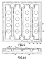
- Fig. 9 is a plan view of a large junction device (i.e. an area greater than or equal to one square millimeter).
- Fig. 10 is a cross section of the device shown in Fig. 9, taken along axis DD.
- Figs. 9 and 10 also illustrate an arrangement of contacts that may be used with any of the epitaxial structures 30 illustrated in Fig. 2 and described above.
- the active region of epitaxial structure 30 is separated into four regions separated by three trenches in which n-contacts 27 are formed. Each region is connected to a submount by four p-submount connections 34 formed on p-contact 26.
- N-contact 27 surrounds the four active regions.
- N-contact 27 is connected to a submount by six n-submount connections 33.
- the n- and p-contacts may be electrically isolated by an insulating layer 32.
- Fig. 11 is an exploded view of a packaged light emitting device.
- a heat-sinking slug 100 is placed into an insert-molded leadframe.
- the insert-molded leadframe is, for example, a filled plastic material 105 molded around a metal frame 106 that provides an electrical path.
- Slug 100 may include an optional reflector cup 102.
- the light emitting device die 104 which may be any of the devices described above, is mounted directly or indirectly via a thermally conducting submount 103 to slug 100.
- An optical lens 108 may be added.
- Reducing the effect of polarization fields on the active region may have several advantages.
- First, carrier recombination rate may increase, increasing the quantum efficiency of the device.
- Second, the carrier recombination lifetime may be reduced, reducing the carrier density at a given current density, and resulting in improved quantum efficiency at increased drive currents.
- Third, electron and hole injection efficiency may increase, leading to more uniform filling of the active region with carriers. Each of these effects may improve the efficiency of the device.
Landscapes
- Led Devices (AREA)
- Led Device Packages (AREA)
Applications Claiming Priority (2)
| Application Number | Priority Date | Filing Date | Title |
|---|---|---|---|
| US769260 | 1996-12-18 | ||
| US10/769,260 US7115908B2 (en) | 2004-01-30 | 2004-01-30 | III-nitride light emitting device with reduced polarization fields |
Publications (3)
| Publication Number | Publication Date |
|---|---|
| EP1560276A2 true EP1560276A2 (fr) | 2005-08-03 |
| EP1560276A3 EP1560276A3 (fr) | 2010-12-01 |
| EP1560276B1 EP1560276B1 (fr) | 2015-10-21 |
Family
ID=34654383
Family Applications (1)
| Application Number | Title | Priority Date | Filing Date |
|---|---|---|---|
| EP05100413.3A Expired - Lifetime EP1560276B1 (fr) | 2004-01-30 | 2005-01-24 | Dispositif émettant de lumière fabriqué de matériau III-nitrure ayant des champs de polarisation réduits |
Country Status (4)
| Country | Link |
|---|---|
| US (1) | US7115908B2 (fr) |
| EP (1) | EP1560276B1 (fr) |
| JP (1) | JP2005217415A (fr) |
| TW (1) | TWI392106B (fr) |
Cited By (2)
| Publication number | Priority date | Publication date | Assignee | Title |
|---|---|---|---|---|
| US8847252B2 (en) | 2005-08-24 | 2014-09-30 | Philips Lumileds Lighting Company, Llc | III-nitride light emitting device with double heterostructure light emitting region |
| WO2016020348A1 (fr) * | 2014-08-04 | 2016-02-11 | Osram Opto Semiconductors Gmbh | Composant optoélectronique et procédé servant à fabriquer ledit composant optoélectronique |
Families Citing this family (51)
| Publication number | Priority date | Publication date | Assignee | Title |
|---|---|---|---|---|
| US7115908B2 (en) * | 2004-01-30 | 2006-10-03 | Philips Lumileds Lighting Company, Llc | III-nitride light emitting device with reduced polarization fields |
| US7332365B2 (en) * | 2004-05-18 | 2008-02-19 | Cree, Inc. | Method for fabricating group-III nitride devices and devices fabricated using method |
| US7791061B2 (en) | 2004-05-18 | 2010-09-07 | Cree, Inc. | External extraction light emitting diode based upon crystallographic faceted surfaces |
| JP2007188990A (ja) * | 2006-01-12 | 2007-07-26 | Mitsubishi Electric Corp | 窒化物半導体素子 |
| JP2007305965A (ja) * | 2006-04-14 | 2007-11-22 | Toyoda Gosei Co Ltd | 発光素子およびこれを用いた通信装置 |
| JP4836703B2 (ja) | 2006-07-31 | 2011-12-14 | パナソニック株式会社 | 半導体レーザおよびその製造方法 |
| US20080283854A1 (en) * | 2007-05-01 | 2008-11-20 | The Regents Of The University Of California | Light emitting diode device layer structure using an indium gallium nitride contact layer |
| US8546846B2 (en) * | 2007-08-20 | 2013-10-01 | Samsung Electronics Co., Ltd. | Nitride semiconductor light emitting device |
| US20090050874A1 (en) | 2007-08-20 | 2009-02-26 | Samsung Electro-Mechanics Co., Ltd. | Nitride semiconductor light emitting device |
| KR100961108B1 (ko) | 2007-11-27 | 2010-06-07 | 삼성엘이디 주식회사 | 분극 현상을 방지한 질화물 반도체 발광 소자 |
| EP3525301B1 (fr) * | 2007-12-28 | 2021-11-03 | Avago Technologies International Sales Pte. Limited | Dispositif doté d'une région active dopée delta |
| JP2011511463A (ja) * | 2008-02-01 | 2011-04-07 | ザ リージェンツ オブ ザ ユニバーシティ オブ カリフォルニア | インジウム混和の増加による、窒化物発光ダイオードの偏光の向上 |
| JP2011511462A (ja) * | 2008-02-01 | 2011-04-07 | ザ リージェンツ オブ ザ ユニバーシティ オブ カリフォルニア | ウエハの軸外カットによる窒化物発光ダイオードの偏光の向上 |
| US8664747B2 (en) * | 2008-04-28 | 2014-03-04 | Toshiba Techno Center Inc. | Trenched substrate for crystal growth and wafer bonding |
| KR100957724B1 (ko) | 2008-06-05 | 2010-05-12 | 우리엘에스티 주식회사 | 화합물 반도체 발광소자 및 발광소자를 위한 발광소자의화합물 반도체 조성비 결정방법 |
| TW201007981A (en) * | 2008-08-11 | 2010-02-16 | Advanced Optoelectronic Tech | Light emitting device and reduced polarization interlayer thereof |
| KR101053799B1 (ko) | 2009-01-09 | 2011-08-03 | 우리엘에스티 주식회사 | 질화물계 발광소자 |
| US8253145B2 (en) * | 2009-04-29 | 2012-08-28 | University Of Seoul Industry Cooperation Foundation | Semiconductor device having strong excitonic binding |
| US20100270547A1 (en) * | 2009-04-27 | 2010-10-28 | University Of Seoul Industry Cooperation Foundation | Semiconductor device |
| CN102460739A (zh) * | 2009-06-05 | 2012-05-16 | 加利福尼亚大学董事会 | 长波长非极性及半极性(Al,Ga,In)N基激光二极管 |
| US8207547B2 (en) | 2009-06-10 | 2012-06-26 | Brudgelux, Inc. | Thin-film LED with P and N contacts electrically isolated from the substrate |
| TWI405409B (zh) * | 2009-08-27 | 2013-08-11 | Novatek Microelectronics Corp | 低電壓差動訊號輸出級 |
| US8525221B2 (en) | 2009-11-25 | 2013-09-03 | Toshiba Techno Center, Inc. | LED with improved injection efficiency |
| JP2011166108A (ja) * | 2010-01-15 | 2011-08-25 | Ricoh Co Ltd | 面発光レーザ素子、面発光レーザアレイ、光走査装置及び画像形成装置 |
| US9252330B2 (en) * | 2010-08-06 | 2016-02-02 | Panasonic Intellectual Property Management Co., Ltd. | Semiconductor light emitting element |
| US8395165B2 (en) | 2011-07-08 | 2013-03-12 | Bridelux, Inc. | Laterally contacted blue LED with superlattice current spreading layer |
| US20130026480A1 (en) | 2011-07-25 | 2013-01-31 | Bridgelux, Inc. | Nucleation of Aluminum Nitride on a Silicon Substrate Using an Ammonia Preflow |
| US8916906B2 (en) | 2011-07-29 | 2014-12-23 | Kabushiki Kaisha Toshiba | Boron-containing buffer layer for growing gallium nitride on silicon |
| US9343641B2 (en) | 2011-08-02 | 2016-05-17 | Manutius Ip, Inc. | Non-reactive barrier metal for eutectic bonding process |
| US8865565B2 (en) | 2011-08-02 | 2014-10-21 | Kabushiki Kaisha Toshiba | LED having a low defect N-type layer that has grown on a silicon substrate |
| US9012939B2 (en) | 2011-08-02 | 2015-04-21 | Kabushiki Kaisha Toshiba | N-type gallium-nitride layer having multiple conductive intervening layers |
| US9142743B2 (en) | 2011-08-02 | 2015-09-22 | Kabushiki Kaisha Toshiba | High temperature gold-free wafer bonding for light emitting diodes |
| US20130032810A1 (en) | 2011-08-03 | 2013-02-07 | Bridgelux, Inc. | Led on silicon substrate using zinc-sulfide as buffer layer |
| US8564010B2 (en) | 2011-08-04 | 2013-10-22 | Toshiba Techno Center Inc. | Distributed current blocking structures for light emitting diodes |
| US8624482B2 (en) | 2011-09-01 | 2014-01-07 | Toshiba Techno Center Inc. | Distributed bragg reflector for reflecting light of multiple wavelengths from an LED |
| US8669585B1 (en) | 2011-09-03 | 2014-03-11 | Toshiba Techno Center Inc. | LED that has bounding silicon-doped regions on either side of a strain release layer |
| US8558247B2 (en) | 2011-09-06 | 2013-10-15 | Toshiba Techno Center Inc. | GaN LEDs with improved area and method for making the same |
| US8686430B2 (en) | 2011-09-07 | 2014-04-01 | Toshiba Techno Center Inc. | Buffer layer for GaN-on-Si LED |
| US20130082274A1 (en) | 2011-09-29 | 2013-04-04 | Bridgelux, Inc. | Light emitting devices having dislocation density maintaining buffer layers |
| US8698163B2 (en) | 2011-09-29 | 2014-04-15 | Toshiba Techno Center Inc. | P-type doping layers for use with light emitting devices |
| US8664679B2 (en) | 2011-09-29 | 2014-03-04 | Toshiba Techno Center Inc. | Light emitting devices having light coupling layers with recessed electrodes |
| US8853668B2 (en) | 2011-09-29 | 2014-10-07 | Kabushiki Kaisha Toshiba | Light emitting regions for use with light emitting devices |
| US9012921B2 (en) | 2011-09-29 | 2015-04-21 | Kabushiki Kaisha Toshiba | Light emitting devices having light coupling layers |
| US9178114B2 (en) | 2011-09-29 | 2015-11-03 | Manutius Ip, Inc. | P-type doping layers for use with light emitting devices |
| US8581267B2 (en) | 2011-11-09 | 2013-11-12 | Toshiba Techno Center Inc. | Series connected segmented LED |
| US8552465B2 (en) | 2011-11-09 | 2013-10-08 | Toshiba Techno Center Inc. | Method for reducing stress in epitaxial growth |
| US8896008B2 (en) | 2013-04-23 | 2014-11-25 | Cree, Inc. | Light emitting diodes having group III nitride surface features defined by a mask and crystal planes |
| KR20150025264A (ko) | 2013-08-28 | 2015-03-10 | 삼성전자주식회사 | 정공주입층을 구비하는 반도체 발광 소자 및 그 제조 방법 |
| TWI577046B (zh) * | 2014-12-23 | 2017-04-01 | 錼創科技股份有限公司 | 半導體發光元件及其製作方法 |
| US10693038B2 (en) | 2017-11-22 | 2020-06-23 | Epistar Corporation | Semiconductor device |
| CN110854248B (zh) * | 2019-12-16 | 2024-07-26 | 广东省半导体产业技术研究院 | 一种光电器件结构及其制作方法 |
Family Cites Families (13)
| Publication number | Priority date | Publication date | Assignee | Title |
|---|---|---|---|---|
| US6459100B1 (en) * | 1998-09-16 | 2002-10-01 | Cree, Inc. | Vertical geometry ingan LED |
| JP2000277868A (ja) * | 1999-03-25 | 2000-10-06 | Sanyo Electric Co Ltd | 発光素子 |
| JP3656456B2 (ja) * | 1999-04-21 | 2005-06-08 | 日亜化学工業株式会社 | 窒化物半導体素子 |
| US6515313B1 (en) * | 1999-12-02 | 2003-02-04 | Cree Lighting Company | High efficiency light emitters with reduced polarization-induced charges |
| US6853663B2 (en) * | 2000-06-02 | 2005-02-08 | Agilent Technologies, Inc. | Efficiency GaN-based light emitting devices |
| US6764888B2 (en) * | 2000-09-27 | 2004-07-20 | Sensor Electronic Technology, Inc. | Method of producing nitride-based heterostructure devices |
| US6635904B2 (en) * | 2001-03-29 | 2003-10-21 | Lumileds Lighting U.S., Llc | Indium gallium nitride smoothing structures for III-nitride devices |
| US6955933B2 (en) * | 2001-07-24 | 2005-10-18 | Lumileds Lighting U.S., Llc | Light emitting diodes with graded composition active regions |
| US6833564B2 (en) * | 2001-11-02 | 2004-12-21 | Lumileds Lighting U.S., Llc | Indium gallium nitride separate confinement heterostructure light emitting devices |
| JP2003234545A (ja) * | 2002-02-07 | 2003-08-22 | Sanyo Electric Co Ltd | 半導体発光素子 |
| WO2003089695A1 (fr) * | 2002-04-15 | 2003-10-30 | The Regents Of The University Of California | Films minces de nitrure de gallium a plan a non polaire obtenus par depot chimique en phase vapeur metalorganique |
| TWI234915B (en) * | 2002-11-18 | 2005-06-21 | Pioneer Corp | Semiconductor light-emitting element and method of manufacturing the same |
| US7115908B2 (en) * | 2004-01-30 | 2006-10-03 | Philips Lumileds Lighting Company, Llc | III-nitride light emitting device with reduced polarization fields |
-
2004
- 2004-01-30 US US10/769,260 patent/US7115908B2/en not_active Expired - Lifetime
-
2005
- 2005-01-24 EP EP05100413.3A patent/EP1560276B1/fr not_active Expired - Lifetime
- 2005-01-27 TW TW094102469A patent/TWI392106B/zh not_active IP Right Cessation
- 2005-01-28 JP JP2005020611A patent/JP2005217415A/ja active Pending
Cited By (6)
| Publication number | Priority date | Publication date | Assignee | Title |
|---|---|---|---|---|
| US8847252B2 (en) | 2005-08-24 | 2014-09-30 | Philips Lumileds Lighting Company, Llc | III-nitride light emitting device with double heterostructure light emitting region |
| US9640724B2 (en) | 2005-08-24 | 2017-05-02 | Lumileds Llc | III-nitride light emitting device with double heterostructure light emitting region |
| WO2016020348A1 (fr) * | 2014-08-04 | 2016-02-11 | Osram Opto Semiconductors Gmbh | Composant optoélectronique et procédé servant à fabriquer ledit composant optoélectronique |
| CN107004739A (zh) * | 2014-08-04 | 2017-08-01 | 奥斯兰姆奥普托半导体有限责任公司 | 光电组件以及用于制造所述光电组件的方法 |
| US9818910B2 (en) | 2014-08-04 | 2017-11-14 | Osram Opto Semiconductors Gmbh | Optoelectronic component and method for the production thereof |
| CN107004739B (zh) * | 2014-08-04 | 2020-03-20 | 奥斯兰姆奥普托半导体有限责任公司 | 光电组件以及用于制造所述光电组件的方法 |
Also Published As
| Publication number | Publication date |
|---|---|
| US7115908B2 (en) | 2006-10-03 |
| JP2005217415A (ja) | 2005-08-11 |
| EP1560276A3 (fr) | 2010-12-01 |
| TWI392106B (zh) | 2013-04-01 |
| EP1560276B1 (fr) | 2015-10-21 |
| TW200537712A (en) | 2005-11-16 |
| US20050169333A1 (en) | 2005-08-04 |
Similar Documents
| Publication | Publication Date | Title |
|---|---|---|
| US7115908B2 (en) | III-nitride light emitting device with reduced polarization fields | |
| EP1560277B1 (fr) | Dispositifs émettants de lumière fabriqués de matériau III-nitrure plus efficace aux courants forts | |
| KR100267839B1 (ko) | 질화물 반도체 장치 | |
| US8106403B2 (en) | III-nitride light emitting device incorporation boron | |
| US9620671B2 (en) | Nitride semiconductor light emitting element and method for manufacturing same | |
| US7939833B2 (en) | Nitride semiconductor light emitting device | |
| US6989555B2 (en) | Strain-controlled III-nitride light emitting device | |
| US7122839B2 (en) | Semiconductor light emitting devices with graded composition light emitting layers | |
| US20080042161A1 (en) | Nitride semiconductor light emitting diode | |
| US7285799B2 (en) | Semiconductor light emitting devices including in-plane light emitting layers | |
| US7851808B2 (en) | Nitride semiconductor light emitting diode | |
| US20260068369A1 (en) | UV-LED with Cathode with Electron Gas Layer |
Legal Events
| Date | Code | Title | Description |
|---|---|---|---|
| PUAI | Public reference made under article 153(3) epc to a published international application that has entered the european phase |
Free format text: ORIGINAL CODE: 0009012 |
|
| AK | Designated contracting states |
Kind code of ref document: A2 Designated state(s): AT BE BG CH CY CZ DE DK EE ES FI FR GB GR HU IE IS IT LI LT LU MC NL PL PT RO SE SI SK TR |
|
| AX | Request for extension of the european patent |
Extension state: AL BA HR LV MK YU |
|
| RAP1 | Party data changed (applicant data changed or rights of an application transferred) |
Owner name: PHILIPS LUMILEDS LIGHTING COMPANY LLC |
|
| PUAL | Search report despatched |
Free format text: ORIGINAL CODE: 0009013 |
|
| AK | Designated contracting states |
Kind code of ref document: A3 Designated state(s): AT BE BG CH CY CZ DE DK EE ES FI FR GB GR HU IE IS IT LI LT LU MC NL PL PT RO SE SI SK TR |
|
| AX | Request for extension of the european patent |
Extension state: AL BA HR LV MK YU |
|
| 17P | Request for examination filed |
Effective date: 20110601 |
|
| AKX | Designation fees paid |
Designated state(s): AT BE BG CH CY CZ DE DK EE ES FI FR GB GR HU IE IS IT LI LT LU MC NL PL PT RO SE SI SK TR |
|
| 17Q | First examination report despatched |
Effective date: 20110927 |
|
| REG | Reference to a national code |
Ref country code: DE Ref legal event code: R079 Ref document number: 602005047729 Country of ref document: DE Free format text: PREVIOUS MAIN CLASS: H01L0033000000 Ipc: H01L0033320000 |
|
| GRAP | Despatch of communication of intention to grant a patent |
Free format text: ORIGINAL CODE: EPIDOSNIGR1 |
|
| RIC1 | Information provided on ipc code assigned before grant |
Ipc: H01L 33/32 20100101AFI20150508BHEP |
|
| INTG | Intention to grant announced |
Effective date: 20150529 |
|
| GRAS | Grant fee paid |
Free format text: ORIGINAL CODE: EPIDOSNIGR3 |
|
| GRAA | (expected) grant |
Free format text: ORIGINAL CODE: 0009210 |
|
| AK | Designated contracting states |
Kind code of ref document: B1 Designated state(s): AT BE BG CH CY CZ DE DK EE ES FI FR GB GR HU IE IS IT LI LT LU MC NL PL PT RO SE SI SK TR |
|
| REG | Reference to a national code |
Ref country code: GB Ref legal event code: FG4D Ref country code: NL Ref legal event code: MP Effective date: 20151021 Ref country code: DE Ref legal event code: R081 Ref document number: 602005047729 Country of ref document: DE Owner name: LUMILEDS HOLDING B.V., NL Free format text: FORMER OWNER: LUMILEDS LIGHTING U.S., LLC, SAN JOSE, CALIF., US |
|
| REG | Reference to a national code |
Ref country code: CH Ref legal event code: EP |
|
| REG | Reference to a national code |
Ref country code: AT Ref legal event code: REF Ref document number: 757093 Country of ref document: AT Kind code of ref document: T Effective date: 20151115 |
|
| REG | Reference to a national code |
Ref country code: IE Ref legal event code: FG4D |
|
| REG | Reference to a national code |
Ref country code: DE Ref legal event code: R096 Ref document number: 602005047729 Country of ref document: DE |
|
| REG | Reference to a national code |
Ref country code: FR Ref legal event code: PLFP Year of fee payment: 12 |
|
| REG | Reference to a national code |
Ref country code: LT Ref legal event code: MG4D |
|
| REG | Reference to a national code |
Ref country code: AT Ref legal event code: MK05 Ref document number: 757093 Country of ref document: AT Kind code of ref document: T Effective date: 20151021 |
|
| PG25 | Lapsed in a contracting state [announced via postgrant information from national office to epo] |
Ref country code: IT Free format text: LAPSE BECAUSE OF FAILURE TO SUBMIT A TRANSLATION OF THE DESCRIPTION OR TO PAY THE FEE WITHIN THE PRESCRIBED TIME-LIMIT Effective date: 20151021 Ref country code: ES Free format text: LAPSE BECAUSE OF FAILURE TO SUBMIT A TRANSLATION OF THE DESCRIPTION OR TO PAY THE FEE WITHIN THE PRESCRIBED TIME-LIMIT Effective date: 20151021 Ref country code: IS Free format text: LAPSE BECAUSE OF FAILURE TO SUBMIT A TRANSLATION OF THE DESCRIPTION OR TO PAY THE FEE WITHIN THE PRESCRIBED TIME-LIMIT Effective date: 20160221 Ref country code: LT Free format text: LAPSE BECAUSE OF FAILURE TO SUBMIT A TRANSLATION OF THE DESCRIPTION OR TO PAY THE FEE WITHIN THE PRESCRIBED TIME-LIMIT Effective date: 20151021 Ref country code: NL Free format text: LAPSE BECAUSE OF FAILURE TO SUBMIT A TRANSLATION OF THE DESCRIPTION OR TO PAY THE FEE WITHIN THE PRESCRIBED TIME-LIMIT Effective date: 20151021 |
|
| PG25 | Lapsed in a contracting state [announced via postgrant information from national office to epo] |
Ref country code: FI Free format text: LAPSE BECAUSE OF FAILURE TO SUBMIT A TRANSLATION OF THE DESCRIPTION OR TO PAY THE FEE WITHIN THE PRESCRIBED TIME-LIMIT Effective date: 20151021 Ref country code: GR Free format text: LAPSE BECAUSE OF FAILURE TO SUBMIT A TRANSLATION OF THE DESCRIPTION OR TO PAY THE FEE WITHIN THE PRESCRIBED TIME-LIMIT Effective date: 20160122 Ref country code: PT Free format text: LAPSE BECAUSE OF FAILURE TO SUBMIT A TRANSLATION OF THE DESCRIPTION OR TO PAY THE FEE WITHIN THE PRESCRIBED TIME-LIMIT Effective date: 20160222 Ref country code: PL Free format text: LAPSE BECAUSE OF FAILURE TO SUBMIT A TRANSLATION OF THE DESCRIPTION OR TO PAY THE FEE WITHIN THE PRESCRIBED TIME-LIMIT Effective date: 20151021 Ref country code: BE Free format text: LAPSE BECAUSE OF NON-PAYMENT OF DUE FEES Effective date: 20160131 Ref country code: SE Free format text: LAPSE BECAUSE OF FAILURE TO SUBMIT A TRANSLATION OF THE DESCRIPTION OR TO PAY THE FEE WITHIN THE PRESCRIBED TIME-LIMIT Effective date: 20151021 Ref country code: AT Free format text: LAPSE BECAUSE OF FAILURE TO SUBMIT A TRANSLATION OF THE DESCRIPTION OR TO PAY THE FEE WITHIN THE PRESCRIBED TIME-LIMIT Effective date: 20151021 |
|
| REG | Reference to a national code |
Ref country code: DE Ref legal event code: R097 Ref document number: 602005047729 Country of ref document: DE |
|
| PG25 | Lapsed in a contracting state [announced via postgrant information from national office to epo] |
Ref country code: CZ Free format text: LAPSE BECAUSE OF FAILURE TO SUBMIT A TRANSLATION OF THE DESCRIPTION OR TO PAY THE FEE WITHIN THE PRESCRIBED TIME-LIMIT Effective date: 20151021 |
|
| PLBE | No opposition filed within time limit |
Free format text: ORIGINAL CODE: 0009261 |
|
| STAA | Information on the status of an ep patent application or granted ep patent |
Free format text: STATUS: NO OPPOSITION FILED WITHIN TIME LIMIT |
|
| PG25 | Lapsed in a contracting state [announced via postgrant information from national office to epo] |
Ref country code: EE Free format text: LAPSE BECAUSE OF FAILURE TO SUBMIT A TRANSLATION OF THE DESCRIPTION OR TO PAY THE FEE WITHIN THE PRESCRIBED TIME-LIMIT Effective date: 20151021 Ref country code: LU Free format text: LAPSE BECAUSE OF FAILURE TO SUBMIT A TRANSLATION OF THE DESCRIPTION OR TO PAY THE FEE WITHIN THE PRESCRIBED TIME-LIMIT Effective date: 20160124 Ref country code: SK Free format text: LAPSE BECAUSE OF FAILURE TO SUBMIT A TRANSLATION OF THE DESCRIPTION OR TO PAY THE FEE WITHIN THE PRESCRIBED TIME-LIMIT Effective date: 20151021 Ref country code: DK Free format text: LAPSE BECAUSE OF FAILURE TO SUBMIT A TRANSLATION OF THE DESCRIPTION OR TO PAY THE FEE WITHIN THE PRESCRIBED TIME-LIMIT Effective date: 20151021 Ref country code: RO Free format text: LAPSE BECAUSE OF FAILURE TO SUBMIT A TRANSLATION OF THE DESCRIPTION OR TO PAY THE FEE WITHIN THE PRESCRIBED TIME-LIMIT Effective date: 20151021 |
|
| REG | Reference to a national code |
Ref country code: CH Ref legal event code: PL |
|
| 26N | No opposition filed |
Effective date: 20160722 |
|
| PG25 | Lapsed in a contracting state [announced via postgrant information from national office to epo] |
Ref country code: MC Free format text: LAPSE BECAUSE OF FAILURE TO SUBMIT A TRANSLATION OF THE DESCRIPTION OR TO PAY THE FEE WITHIN THE PRESCRIBED TIME-LIMIT Effective date: 20151021 |
|
| PG25 | Lapsed in a contracting state [announced via postgrant information from national office to epo] |
Ref country code: LI Free format text: LAPSE BECAUSE OF NON-PAYMENT OF DUE FEES Effective date: 20160131 Ref country code: CH Free format text: LAPSE BECAUSE OF NON-PAYMENT OF DUE FEES Effective date: 20160131 |
|
| REG | Reference to a national code |
Ref country code: IE Ref legal event code: MM4A |
|
| PG25 | Lapsed in a contracting state [announced via postgrant information from national office to epo] |
Ref country code: SI Free format text: LAPSE BECAUSE OF FAILURE TO SUBMIT A TRANSLATION OF THE DESCRIPTION OR TO PAY THE FEE WITHIN THE PRESCRIBED TIME-LIMIT Effective date: 20151021 |
|
| PG25 | Lapsed in a contracting state [announced via postgrant information from national office to epo] |
Ref country code: BE Free format text: LAPSE BECAUSE OF FAILURE TO SUBMIT A TRANSLATION OF THE DESCRIPTION OR TO PAY THE FEE WITHIN THE PRESCRIBED TIME-LIMIT Effective date: 20151021 |
|
| REG | Reference to a national code |
Ref country code: FR Ref legal event code: PLFP Year of fee payment: 13 |
|
| PG25 | Lapsed in a contracting state [announced via postgrant information from national office to epo] |
Ref country code: IE Free format text: LAPSE BECAUSE OF NON-PAYMENT OF DUE FEES Effective date: 20160124 |
|
| REG | Reference to a national code |
Ref country code: FR Ref legal event code: PLFP Year of fee payment: 14 |
|
| REG | Reference to a national code |
Ref country code: DE Ref legal event code: R081 Ref document number: 602005047729 Country of ref document: DE Owner name: LUMILEDS HOLDING B.V., NL Free format text: FORMER OWNER: PHILIPS LUMILEDS LIGHTING COMPANY, LLC, SAN JOSE, CALIF, US |
|
| PG25 | Lapsed in a contracting state [announced via postgrant information from national office to epo] |
Ref country code: HU Free format text: LAPSE BECAUSE OF FAILURE TO SUBMIT A TRANSLATION OF THE DESCRIPTION OR TO PAY THE FEE WITHIN THE PRESCRIBED TIME-LIMIT; INVALID AB INITIO Effective date: 20050124 Ref country code: CY Free format text: LAPSE BECAUSE OF FAILURE TO SUBMIT A TRANSLATION OF THE DESCRIPTION OR TO PAY THE FEE WITHIN THE PRESCRIBED TIME-LIMIT Effective date: 20151021 |
|
| PG25 | Lapsed in a contracting state [announced via postgrant information from national office to epo] |
Ref country code: TR Free format text: LAPSE BECAUSE OF FAILURE TO SUBMIT A TRANSLATION OF THE DESCRIPTION OR TO PAY THE FEE WITHIN THE PRESCRIBED TIME-LIMIT Effective date: 20151021 |
|
| PG25 | Lapsed in a contracting state [announced via postgrant information from national office to epo] |
Ref country code: BG Free format text: LAPSE BECAUSE OF FAILURE TO SUBMIT A TRANSLATION OF THE DESCRIPTION OR TO PAY THE FEE WITHIN THE PRESCRIBED TIME-LIMIT Effective date: 20151021 |
|
| REG | Reference to a national code |
Ref country code: GB Ref legal event code: 732E Free format text: REGISTERED BETWEEN 20180920 AND 20180926 |
|
| P01 | Opt-out of the competence of the unified patent court (upc) registered |
Effective date: 20230530 |
|
| PGFP | Annual fee paid to national office [announced via postgrant information from national office to epo] |
Ref country code: DE Payment date: 20240129 Year of fee payment: 20 Ref country code: GB Payment date: 20240123 Year of fee payment: 20 |
|
| PGFP | Annual fee paid to national office [announced via postgrant information from national office to epo] |
Ref country code: FR Payment date: 20240125 Year of fee payment: 20 |
|
| REG | Reference to a national code |
Ref country code: DE Ref legal event code: R079 Ref document number: 602005047729 Country of ref document: DE Free format text: PREVIOUS MAIN CLASS: H01L0033320000 Ipc: H10H0020825000 |
|
| REG | Reference to a national code |
Ref country code: DE Ref legal event code: R071 Ref document number: 602005047729 Country of ref document: DE |
|
| REG | Reference to a national code |
Ref country code: GB Ref legal event code: PE20 Expiry date: 20250123 |
|
| PG25 | Lapsed in a contracting state [announced via postgrant information from national office to epo] |
Ref country code: GB Free format text: LAPSE BECAUSE OF EXPIRATION OF PROTECTION Effective date: 20250123 |