EP1560279B1 - Elément piezoélectrique et procédé de fabrication, tête jet d'encre et dispositif d'enregistrement à jet d'encre utilisant l'élément - Google Patents
Elément piezoélectrique et procédé de fabrication, tête jet d'encre et dispositif d'enregistrement à jet d'encre utilisant l'élément Download PDFInfo
- Publication number
- EP1560279B1 EP1560279B1 EP05001581A EP05001581A EP1560279B1 EP 1560279 B1 EP1560279 B1 EP 1560279B1 EP 05001581 A EP05001581 A EP 05001581A EP 05001581 A EP05001581 A EP 05001581A EP 1560279 B1 EP1560279 B1 EP 1560279B1
- Authority
- EP
- European Patent Office
- Prior art keywords
- thin film
- piezoelectric element
- lead
- piezoelectric
- titanate
- Prior art date
- Legal status (The legal status is an assumption and is not a legal conclusion. Google has not performed a legal analysis and makes no representation as to the accuracy of the status listed.)
- Expired - Lifetime
Links
Images



Classifications
-
- B—PERFORMING OPERATIONS; TRANSPORTING
- B41—PRINTING; LINING MACHINES; TYPEWRITERS; STAMPS
- B41J—TYPEWRITERS; SELECTIVE PRINTING MECHANISMS, i.e. MECHANISMS PRINTING OTHERWISE THAN FROM A FORME; CORRECTION OF TYPOGRAPHICAL ERRORS
- B41J2/00—Typewriters or selective printing mechanisms characterised by the printing or marking process for which they are designed
- B41J2/005—Typewriters or selective printing mechanisms characterised by the printing or marking process for which they are designed characterised by bringing liquid or particles selectively into contact with a printing material
- B41J2/01—Ink jet
- B41J2/135—Nozzles
- B41J2/16—Production of nozzles
- B41J2/1621—Manufacturing processes
- B41J2/164—Manufacturing processes thin film formation
- B41J2/1646—Manufacturing processes thin film formation thin film formation by sputtering
-
- B—PERFORMING OPERATIONS; TRANSPORTING
- B41—PRINTING; LINING MACHINES; TYPEWRITERS; STAMPS
- B41J—TYPEWRITERS; SELECTIVE PRINTING MECHANISMS, i.e. MECHANISMS PRINTING OTHERWISE THAN FROM A FORME; CORRECTION OF TYPOGRAPHICAL ERRORS
- B41J2/00—Typewriters or selective printing mechanisms characterised by the printing or marking process for which they are designed
- B41J2/005—Typewriters or selective printing mechanisms characterised by the printing or marking process for which they are designed characterised by bringing liquid or particles selectively into contact with a printing material
- B41J2/01—Ink jet
- B41J2/135—Nozzles
- B41J2/16—Production of nozzles
- B41J2/1607—Production of print heads with piezoelectric elements
- B41J2/161—Production of print heads with piezoelectric elements of film type, deformed by bending and disposed on a diaphragm
-
- B—PERFORMING OPERATIONS; TRANSPORTING
- B41—PRINTING; LINING MACHINES; TYPEWRITERS; STAMPS
- B41J—TYPEWRITERS; SELECTIVE PRINTING MECHANISMS, i.e. MECHANISMS PRINTING OTHERWISE THAN FROM A FORME; CORRECTION OF TYPOGRAPHICAL ERRORS
- B41J2/00—Typewriters or selective printing mechanisms characterised by the printing or marking process for which they are designed
- B41J2/005—Typewriters or selective printing mechanisms characterised by the printing or marking process for which they are designed characterised by bringing liquid or particles selectively into contact with a printing material
- B41J2/01—Ink jet
- B41J2/135—Nozzles
- B41J2/16—Production of nozzles
- B41J2/1621—Manufacturing processes
- B41J2/1623—Manufacturing processes bonding and adhesion
-
- B—PERFORMING OPERATIONS; TRANSPORTING
- B41—PRINTING; LINING MACHINES; TYPEWRITERS; STAMPS
- B41J—TYPEWRITERS; SELECTIVE PRINTING MECHANISMS, i.e. MECHANISMS PRINTING OTHERWISE THAN FROM A FORME; CORRECTION OF TYPOGRAPHICAL ERRORS
- B41J2/00—Typewriters or selective printing mechanisms characterised by the printing or marking process for which they are designed
- B41J2/005—Typewriters or selective printing mechanisms characterised by the printing or marking process for which they are designed characterised by bringing liquid or particles selectively into contact with a printing material
- B41J2/01—Ink jet
- B41J2/135—Nozzles
- B41J2/16—Production of nozzles
- B41J2/1621—Manufacturing processes
- B41J2/1626—Manufacturing processes etching
- B41J2/1628—Manufacturing processes etching dry etching
-
- B—PERFORMING OPERATIONS; TRANSPORTING
- B41—PRINTING; LINING MACHINES; TYPEWRITERS; STAMPS
- B41J—TYPEWRITERS; SELECTIVE PRINTING MECHANISMS, i.e. MECHANISMS PRINTING OTHERWISE THAN FROM A FORME; CORRECTION OF TYPOGRAPHICAL ERRORS
- B41J2/00—Typewriters or selective printing mechanisms characterised by the printing or marking process for which they are designed
- B41J2/005—Typewriters or selective printing mechanisms characterised by the printing or marking process for which they are designed characterised by bringing liquid or particles selectively into contact with a printing material
- B41J2/01—Ink jet
- B41J2/135—Nozzles
- B41J2/16—Production of nozzles
- B41J2/1621—Manufacturing processes
- B41J2/1631—Manufacturing processes photolithography
-
- B—PERFORMING OPERATIONS; TRANSPORTING
- B41—PRINTING; LINING MACHINES; TYPEWRITERS; STAMPS
- B41J—TYPEWRITERS; SELECTIVE PRINTING MECHANISMS, i.e. MECHANISMS PRINTING OTHERWISE THAN FROM A FORME; CORRECTION OF TYPOGRAPHICAL ERRORS
- B41J2/00—Typewriters or selective printing mechanisms characterised by the printing or marking process for which they are designed
- B41J2/005—Typewriters or selective printing mechanisms characterised by the printing or marking process for which they are designed characterised by bringing liquid or particles selectively into contact with a printing material
- B41J2/01—Ink jet
- B41J2/135—Nozzles
- B41J2/16—Production of nozzles
- B41J2/1621—Manufacturing processes
- B41J2/1632—Manufacturing processes machining
-
- B—PERFORMING OPERATIONS; TRANSPORTING
- B41—PRINTING; LINING MACHINES; TYPEWRITERS; STAMPS
- B41J—TYPEWRITERS; SELECTIVE PRINTING MECHANISMS, i.e. MECHANISMS PRINTING OTHERWISE THAN FROM A FORME; CORRECTION OF TYPOGRAPHICAL ERRORS
- B41J2/00—Typewriters or selective printing mechanisms characterised by the printing or marking process for which they are designed
- B41J2/005—Typewriters or selective printing mechanisms characterised by the printing or marking process for which they are designed characterised by bringing liquid or particles selectively into contact with a printing material
- B41J2/01—Ink jet
- B41J2/135—Nozzles
- B41J2/16—Production of nozzles
- B41J2/1621—Manufacturing processes
- B41J2/164—Manufacturing processes thin film formation
- B41J2/1642—Manufacturing processes thin film formation thin film formation by CVD [chemical vapor deposition]
-
- H—ELECTRICITY
- H10—SEMICONDUCTOR DEVICES; ELECTRIC SOLID-STATE DEVICES NOT OTHERWISE PROVIDED FOR
- H10N—ELECTRIC SOLID-STATE DEVICES NOT OTHERWISE PROVIDED FOR
- H10N30/00—Piezoelectric or electrostrictive devices
- H10N30/01—Manufacture or treatment
- H10N30/07—Forming of piezoelectric or electrostrictive parts or bodies on an electrical element or another base
- H10N30/074—Forming of piezoelectric or electrostrictive parts or bodies on an electrical element or another base by depositing piezoelectric or electrostrictive layers, e.g. aerosol or screen printing
- H10N30/076—Forming of piezoelectric or electrostrictive parts or bodies on an electrical element or another base by depositing piezoelectric or electrostrictive layers, e.g. aerosol or screen printing by vapour phase deposition
-
- H—ELECTRICITY
- H10—SEMICONDUCTOR DEVICES; ELECTRIC SOLID-STATE DEVICES NOT OTHERWISE PROVIDED FOR
- H10N—ELECTRIC SOLID-STATE DEVICES NOT OTHERWISE PROVIDED FOR
- H10N30/00—Piezoelectric or electrostrictive devices
- H10N30/20—Piezoelectric or electrostrictive devices with electrical input and mechanical output, e.g. functioning as actuators or vibrators
- H10N30/204—Piezoelectric or electrostrictive devices with electrical input and mechanical output, e.g. functioning as actuators or vibrators using bending displacement, e.g. unimorph, bimorph or multimorph cantilever or membrane benders
- H10N30/2041—Beam type
- H10N30/2042—Cantilevers, i.e. having one fixed end
-
- H—ELECTRICITY
- H10—SEMICONDUCTOR DEVICES; ELECTRIC SOLID-STATE DEVICES NOT OTHERWISE PROVIDED FOR
- H10N—ELECTRIC SOLID-STATE DEVICES NOT OTHERWISE PROVIDED FOR
- H10N30/00—Piezoelectric or electrostrictive devices
- H10N30/704—Piezoelectric or electrostrictive devices based on piezoelectric or electrostrictive films or coatings
-
- H—ELECTRICITY
- H10—SEMICONDUCTOR DEVICES; ELECTRIC SOLID-STATE DEVICES NOT OTHERWISE PROVIDED FOR
- H10N—ELECTRIC SOLID-STATE DEVICES NOT OTHERWISE PROVIDED FOR
- H10N30/00—Piezoelectric or electrostrictive devices
- H10N30/80—Constructional details
- H10N30/85—Piezoelectric or electrostrictive active materials
- H10N30/853—Ceramic compositions
- H10N30/8548—Lead-based oxides
- H10N30/8554—Lead-zirconium titanate [PZT] based
-
- B—PERFORMING OPERATIONS; TRANSPORTING
- B41—PRINTING; LINING MACHINES; TYPEWRITERS; STAMPS
- B41J—TYPEWRITERS; SELECTIVE PRINTING MECHANISMS, i.e. MECHANISMS PRINTING OTHERWISE THAN FROM A FORME; CORRECTION OF TYPOGRAPHICAL ERRORS
- B41J2/00—Typewriters or selective printing mechanisms characterised by the printing or marking process for which they are designed
- B41J2/005—Typewriters or selective printing mechanisms characterised by the printing or marking process for which they are designed characterised by bringing liquid or particles selectively into contact with a printing material
- B41J2/01—Ink jet
- B41J2/135—Nozzles
- B41J2/14—Structure thereof only for on-demand ink jet heads
- B41J2/14201—Structure of print heads with piezoelectric elements
- B41J2/14233—Structure of print heads with piezoelectric elements of film type, deformed by bending and disposed on a diaphragm
- B41J2002/1425—Embedded thin film piezoelectric element
Definitions
- piezoelectric elements are used in the form of thin films whose volumes are significantly reduced from those of sinters, which have conventionally been used in various applications, and active researches and developments have been made for reducing the thickness of piezoelectric elements.
- PZT film formation methods include a sputtering method, a CVD method, a sol-gel method, or the like.
- Piezoelectric elements which contain a lead compound such as PZT are synthesized at high temperature. This is true for piezoelectric elements in the form of thin films.
- a piezoelectric thin film is often made up of a collection of columnar crystal grains oriented from one side to the other side in the thickness direction of the piezoelectric thin film fabricated by a sputtering method, for example.
- the boundaries of these columnar crystal grains exist as grain boundaries. Even a piezoelectric thin film, which is not in the form of a columnar crystal grain collection, also has many grain boundaries.
- the thickness of the piezoelectric thin film is 2 ⁇ m or more but 6 ⁇ m or less.
- the piezoelectric thin film having stable displacement and high reliability in normal use is obtained easily.
- a highly reliable piezoelectric element piezoelectric actuator which is displaced in the film-layering direction of the layered structure by application of a voltage between the first and second electrode films is easily attained.
- the piezoelectric thin film is made of lead zirconate titanate or lead-zirconate-titanate-based oxide, which is an oxide having a perovskite crystalline structure, the lead zirconate titanate having a chemical composition expressed by a chemical formula Pb (1-x) (Zr (1-s) Ti s )O 3 (0 ⁇ s ⁇ 1), the lead-zirconate-titanate-based oxide having a chemical composition expressed by a chemical formula (Pb (1-x-y) A y )(Zr (1-s-t) Ti s B t )O 3 (0 ⁇ s ⁇ 1, 0 ⁇ t ⁇ 1-s) where A is a substitutive metal ion in an A-site in the perovskite crystalline structure and B is a substitutive metal ion in a B-site in the perovskite crystalline structure, the value of x in the chemical composition formulas of the lead zirconate titanate and the lead-zirconate-t
- One method is that when the potential of the substrate is electrically floating so as not to be fixed at the ground potential (i.e., the substrate is not grounded and is not electrically connected to any other members), the degree of vacuum during the sputter deposition process is increased (i.e., the sputtering gas pressure is decreased) so as to reduce the probability of collision between the sputtered particles and the gas molecules present in the space between the substrate and the target, thereby subjecting the substrate to the ion bombardment.
- Alternative method is that the potential of the substrate is made equal to the ground potential or made to be a negative potential lower than the ground potential, so that the sputtered particles are electrically attracted to the substrate, thereby subjecting the substrate to the ion bombardment.
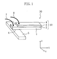
- the first electrode film 2 is made of an iridium (Ir) alloy thin film having a thickness of 0.10 ⁇ m and containing 6 mol% of cobalt (Co), and is formed on and entirely across one surface of the substrate 1 in the thickness direction. It should be noted that the first electrode film 2 does not have to be made of a Co-containing iridium alloy.
- the piezoelectric thin film 3 is formed across the entire upper surface of the first electrode film 2 excluding the 3.0-mm (base) end portion thereof that is bonded to the stainless steel support substrate 5 (i.e., a portion of the upper surface of the first electrode film 2 having a width of 3.0 mm and a length of 8.0 mm), and is made of an oxide having a perovskite crystalline structure.
- the value of x in the chemical composition formulas of the lead zirconate titanate and the lead-zirconate-titanate-based oxide which indicates a deficiency in Pb content in each composition that is a deviation from stoichiometric composition, is more than 0 but not more than 0.15.
- the lead content in the composition of the piezoelectric thin film 3 is thus less than that of the stoichiometric composition. This eliminates, in the grain boundaries in the piezoelectric thin film 3 , the existence of lead oxide that undergoes a chemical reaction with water content in the atmosphere. As a result, even if the piezoelectric element is driven by application of a voltage in a high humidity environment, degradation resulting from insulation deterioration does not occur.
- the character A in the chemical composition formula of the lead-zirconate-titanate-based oxide is preferably at least one metal ion selected from the group consisting of lanthanum (La), strontium (Sr), bismuth (Bi), and calcium (Ca).
- the character B in the chemical composition formula is preferably at least one metal ion selected from the group consisting of niobium (Nb), magnesium (Mg), nickel (Ni), manganese (Mn), and iron (Fe).
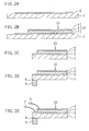
- the substrate 1 whose surface has been polished to be a mirror finished surface and which has a size of 20 mm x 20 mm and a thickness of 0.30 mm is prepared.
- the first electrode film 2 is formed by an RF sputtering method on the substrate 1 by using a stainless steel mask (not shown) having a thickness of 0.2 mm and including therein rectangular openings having a width of 5.0 mm and a length of 18.0 mm.
- the piezoelectric thin film 3 made of the above-mentioned PZT or PZT-based oxide is formed, by an RF magnetron sputtering method, precisely in a predetermined position on the surface of the first electrode film 2 by using a stainless steel mask (thickness: 0.2 mm) including therein rectangular openings having a width of 5.0 mm and a length of 8.0 mm.
- a sinter target of PZT or PZT-based oxide is used.
- the substrate 1 is subjected to ion bombardment. More specifically, when the substrate is in a state in which its potential floats electrically so as not to be fixed at the ground potential, the sputtering gas pressure is set as small as 0.15 Pa or less (but not less than 0.05 Pa for plasma generation) so that the degree of vacuum during the sputter deposition process is increased, thereby reducing the probability of collision between the sputtered particles and the gas molecules present in the space between the substrate 1 and the target.
- the sputtered particles are electrically attracted to the substrate 1 , whereby the substrate 1 is subjected to the ion bombardment. Consequently, among the particles of the composition elements ejected from the target onto the substrate 1 by the sputtering gas during the sputter deposition process, the particles of the lead element having a high vapor pressure are reduced in deposition rate. As a result, the piezoelectric thin film 3 expressed by the above chemical composition formula, in which the lead content is small, is formed easily.
- the first electrode film 2 is made of a noble metal to which an additive such as titanium has been added (cobalt-containing iridium in this embodiment), it becomes easier to preferentially orient the piezoelectric thin film 3 along the (001) plane. More specifically, the additive is present in the form of islands in a dotted pattern on the surface of the first electrode film 2 .
- This additive which is titanium or the like, easily undergoes oxidation. Thus, even if the additive contained is not in the form of oxide, the additive existing in a dotted pattern on the surface becomes an oxide, if oxygen is present in the piezoelectric thin film 3 formation process step or the like.
- one end of the substrate 1 of the piezoelectric element precursor 22 is bonded to the stainless steel support substrate 5 by using the epoxy adhesive 6.
- the piezoelectric element 20 prepared in the above manner was placed in a thermostatic high humidity chamber held in an atmosphere in which the temperature was 35 C° and the relative humidity was 80%, and a direct voltage of 35 V was then applied between the first electrode film 2 and the second electrode film 4 to perform a durability test for 200 hours. Elapsed time since the start of the voltage application and the value of leakage current at the respective elapsed time were measured.
- the external appearance of the electrode film surfaces of the piezoelectric element 20 was observed after the 200-hour durability test by an optical microscope. No changes such as cracks or coloring were observed.
- a triangular voltage with a maximum voltage of 0 V and a minimum voltage of - 25 V was applied between the first electrode film 2 and the second electrode film 4 of the piezoelectric element 20 so as to measure the amount of displacement in up-and-down movement of the tip of the piezoelectric element 20 .
- the applied voltage changed from 0 V to - 25 V
- the tip of the piezoelectric element 20 was linearly displaced from 0 ⁇ m to - 7.2 ⁇ m in proportion to the applied voltage.
- a piezoelectric element 20 was prepared in the same manner as in Example 1.
- the sputtering time for depositing a piezoelectric thin film 3 (PZT thin film) by sputtering was changed to 30 minutes, and in the other respects, a piezoelectric element 20 was prepared in the same manner as in Example 1.
- a silicon substrate with a first electrode film 2 (an iridium alloy thin film) formed thereon was attached onto a metal substrate holder and a ground wire was attached to the substrate holder for connection to the ground potential.
- the substrate 1 was changed to a pyrex glass substrate (coning # 7059).
- a piezoelectric element 20 was prepared in the same manner as in Example 7.
- a triangular voltage with a maximum voltage of 0 V and a minimum voltage of - 25 V was applied between the first electrode film 2 and the second electrode film 4 of the piezoelectric element 20 so as to measure the amount of displacement in up-and-down movement of the tip of the piezoelectric element 20 .
- the applied voltage changed from 0V to - 25V, the tip of the piezoelectric element 20 was linearly displaced from 0 ⁇ m to - 9.3 ⁇ m in proportion to the applied voltage.
- a triangular voltage with a maximum voltage of 0 V and a minimum voltage of - 25 V was applied between the first electrode film 2 and the second electrode film 4 of the piezoelectric element 20 so as to measure the amount of displacement in up-and-down movement of the tip of the piezoelectric element 20 .
- the applied voltage changed from 0V to - 25V, the tip of the piezoelectric element 20 was linearly displaced from 0 ⁇ m to - 5.0 ⁇ m in proportion to the applied voltage.
- the piezoelectric element 20 was subjected to a durability test performed in a thermostatic high humidity chamber in which the temperature was 35 C° and the relative humidity was 80%. From the test results, it was found that the value of leakage current was 0.4 nA, 1.2 nA, 5 nA, and 5nA at the measurement start time, after one hour, after 100 hours, and after 200 hours, respectively. This indicates that the piezoelectric element 20 of this example had high reliability.
- the PZT-based oxide thin film of the piezoelectric element 20 prepared in this manner was a film having a perovskite crystalline structure and preferentially oriented along the (001) plane (the (001) crystalline orientation degree was 85%).
- a silicon substrate with a first electrode film 2 (an iridium alloy thin film) formed thereon was attached onto a substrate holder made of metal, and one end of a lead wire was attached to the substrate holder and the other end of the lead wire was attached to a DC power supply so as to allow the DC power supply to apply to the substrate holder (i.e., the silicon substrate) a negative bias voltage of - 200 V with respect to the ground potential.
- the potential of the silicon substrate, over which the PZT thin film was to be formed was kept at - 200 V with respect to the ground potential.
- a triangular voltage with a maximum voltage of 0 V and a minimum voltage of - 25 V was applied between the first electrode film 2 and the second electrode film 4 of the piezoelectric element 20 so as to measure the amount of displacement in up-and-down movement of the tip of the piezoelectric element 20 .
- the applied voltage changed from 0 V to - 25V, the tip of the piezoelectric element 20 was linearly displaced from 0 ⁇ m to - 6.2 ⁇ m in proportion to the applied voltage.
- the PZT thin film of the piezoelectric element obtained in this manner was a film having a perovskite crystalline structure and preferentially oriented along the (001) plane (the (001) crystalline orientation degree was 97%).
- the thickness of the PZT thin film was 3.5 ⁇ m.
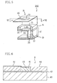
- the actuator section B includes a first electrode film 33 (separate electrode) above each pressure chamber 32 .
- the position of the first electrode film 33 generally corresponds to that of the pressure chamber 32 .
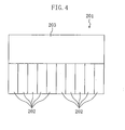
- the ink channel member C includes: a common ink chamber 35 shared by the pressure chambers 32 of the plurality of ink discharging elements 202 arranged in the ink supply direction; a supply port 36 via which the common ink chamber 35 is communicated to the pressure chamber 32 so that ink in the common ink chamber 35 is supplied into the pressure chamber 32 ; and an ink channel 37 through which ink in the pressure chamber 32 is discharged.
- the reference character D denotes a nozzle plate.
- the first electrode film 33 , the piezoelectric thin film 41 and the second electrode film 42 are layered in this order to form a layered structure.
- This layered structure and the vibration plate 43 provided on one surface of the layered structure (i.e., one surface of the layered structure closer to the second electrode film 42 ) in the film-layering direction form a piezoelectric element (piezoelectric actuator).
- the piezoelectric thin film 41 is a PZT thin film which is expressed by Pb 0.97 (Zr 0.53 Ti 0.47 )O 3
- the piezoelectric thin film 41 may be made of any oxide having a perovskite crystalline structure so long as the oxide is made of PZT whose composition is expressed by the chemical formula Pb (1-x) (Zr (1-s) Ti s )O 3 (0 ⁇ s ⁇ 1) or PZT-based oxide expressed by the chemical composition formula (Pb (1-x-y) A y )(Zr (1-s-t) Ti s B t )O 3 (0 ⁇ s ⁇ 1, 0 ⁇ t ⁇ 1-s) and the value of x in the chemical composition formulas of the lead zirconate titanate and the lead-zirconate-titanate-based oxide, which indicates a deficiency in Pb content in each composition that is a deviation from stoichiometric composition, is more than 0 but not more than 0.
- the character "A” in the chemical composition formula of the lead-zirconate-titanate-based oxide is preferably at least one metal ion selected from the group consisting of lanthanum (La), strontium (Sr), bismuth (Bi), and calcium (Ca).
- the character "B” in the chemical composition formula is preferably at least one metal ion selected from the group consisting of niobium (Nb), magnesium (Mg), nickel (Ni), manganese (Mn), and iron (Fe).
- the ink jet recording apparatus 81 includes a plurality of rollers 85 for moving the recording medium 82 in the secondary scanning direction (the direction Y in FIG. 8 ), which is substantially perpendicular to the primary scanning direction X of the ink jet head 201 .
- the plurality of rollers 85 together form relative movement means for relatively moving the ink jet head 201 and the recording medium 82 with respect to each other, while forming recording medium moving means for moving the recording medium 82 in the direction (the secondary scanning direction Y) substantially perpendicular to the predetermined direction.
- an arrow Z represents the vertical direction.
Landscapes
- Engineering & Computer Science (AREA)
- Manufacturing & Machinery (AREA)
- Chemical & Material Sciences (AREA)
- Ceramic Engineering (AREA)
- Particle Formation And Scattering Control In Inkjet Printers (AREA)
- Compositions Of Oxide Ceramics (AREA)
Claims (12)
- Elément piézoélectrique comprenant une structure en couches dans laquelle un premier film d'électrode, un film piézoélectrique mince et un deuxième film d'électrode sont empilés en couches dans cet ordre,
caractérisé en ce que le film piézoélectrique mince est fait de zirconate-titanate de plomb ou d'un oxyde à base de zirconate-titanate de plomb, qui est un oxyde ayant une structure cristalline de type perovskite, le zirconate-titanate de plomb ayant une composition chimique exprimée par la formule chimique Pb(1-x)(Zr(1-s)Tis)O3 (0<s<1), l'oxyde à base de zirconate-titanate de plomb ayant une composition chimique exprimée par la formule chimique (Pb(1-x-y)Ay) (Zr(1-s-t)TisBi)O3 (0<s<1, 0<t<1-s), dans laquelle A est un ion métallique de substitution sur un site A dans la structure cristalline de type perovskite et B est un ion métallique de substitution sur un site B dans la structure cristalline de type perovskite, et
la valeur de x dans les formules de composition chimique du zirconate-titanate de plomb et de l'oxyde à base de zirconate-titanate de plomb, qui indique un défaut de teneur de Pb dans chaque composition, à savoir un écart par rapport à la composition stoechiométrique, est supérieur à 0 mais non supérieur à 0,15. - Elément piézoélectrique selon la revendication 1, dans lequel A dans la formule de composition chimique de l'oxyde à base de zirconate-titanate de plomb est au moins un ion métallique choisi dans le groupe constitué par le lanthane (La), le strontium Sr), le bismuth (Bi) et le calcium (Ca), et
B dans la formule de composition chimique est au moins un ion métallique choisi dans le groupe constitué par le niobium (Nb), le magnésium (Mg), le nickel (Ni), le manganèse (Mn) et le fer (Fe). - Elément piézoélectrique selon la revendication 1, dans lequel l'épaisseur du film piézoélectrique mince est de 2 µm ou plus, mais de 6 µm ou moins.
- Elément piézoélectrique selon la revendication 1, dans lequel le film piézoélectrique mince est de préférence orienté dans un plan (001).
- Elément piézoélectrique selon la revendication 1, dans lequel une plaque de vibration est fournie sur une surface de la structure en couches dans la direction de dépôt de couche de film.
- Elément piézoélectrique selon la revendication 5, dans lequel la plaque de vibration est faite d'au moins un matériau choisi dans le groupe constitué par du silicium, du verre, un matériau céramique et un matériau métallique.
- Procédé de fabrication d'un élément piézoélectrique, comprenant l'étape de formation d'un premier film d'électrode sur un substrat, l'étape de formation d'un film piézoélectrique mince sur le premier film d'électrode par un procédé de pulvérisation cathodique et l'étape de formation d'un deuxième film d'électrode sur le film piézoélectrique mince,
caractérisé en ce que le film piézoélectrique mince est fait de zirconate-titanate de plomb ou d'un oxyde à base de zirconate-titanate de plomb, qui est un oxyde ayant une structure cristalline de type perovskite, le zirconate-titanate de plomb ayant une composition chimique exprimée par la formule chimique Pb(1-x) (Zr(1-s)Tis)O3 (0<s<1), l'oxyde à base de zirconate-titanate de plomb ayant une composition chimique exprimée par la formule chimique (Pb(1-x-y)Ay) (Zr(1-s-t)TisBt)O3 (0<s<1, 0<t<1-s), dans laquelle A est un ion métallique de substitution sur un site A dans la structure cristalline de type perovskite et B est un ion métallique de substitution sur un site B dans la structure cristalline de type perovskite,
la valeur de x dans les formules de composition chimique du zirconate-titanate de plomb et de l'oxyde à base de zirconate-titanate de plomb, qui indique un défaut de teneur de Pb dans chaque composition, à savoir un écart par rapport à la composition stoechiométrique, est supérieur à 0 mais non supérieur à 0,15, et
dans l'étape de formation du film piézoélectrique mince, le film piézoélectrique mince est formé dans des conditions de pulvérisation cathodique dans lesquelles le substrat portant le premier film d'électrode formé sur celui-ci a un potentiel qui flotte au plan électrique de façon à ne pas être fixé au potentiel de la terre, et une pression de gaz de pulvérisation cathodique est de 0,05 Pa ou plus, mais de 0,15 Pa ou moins. - Procédé de fabrication d'un élément piézoélectrique, comprenant l'étape de formation d'un premier film d'électrode sur un substrat, l'étape de formation d'un film piézoélectrique mince sur le premier film d'électrode par un procédé de pulvérisation cathodique et l'étape de formation d'un deuxième film d'électrode sur le film piézoélectrique mince,
caractérisé en ce que le film piézoélectrique mince est fait de zirconate-titanate de plomb ou d'un oxyde à base de zirconate-titanate de plomb, qui est un oxyde ayant une structure cristalline de type perovskite, le zirconate-titanate de plomb ayant une composition chimique exprimée par la formule chimique Pb(1-x) (Zr(1-s)Tis)O3 (0<s<1), l'oxyde à base de zirconate-titanate de plomb ayant une composition chimique exprimée par la formule chimique (Pb(1-x-y)Ay) (Zr(1-s-t)TisBt)O3 (0<s<1, 0<t<1-s), dans laquelle A est un ion métallique de substitution sur un site A dans la structure cristalline de type perovskite et B est un ion métallique de substitution sur un site B dans la structure cristalline de type perovskite,
la valeur de x dans les formules de composition chimique du zirconate-titanate de plomb et de l'oxyde à base de zirconate-titanate de plomb, qui indique un défaut de teneur de Pb dans chaque composition, à savoir un écart par rapport à la composition stoechiométrique, est supérieur à 0 mais non supérieur à 0,15, et
dans l'étape de formation du film piézoélectrique mince, le film piézoélectrique mince est formé dans des conditions de pulvérisation cathodique dans lesquelles une tension de polarisation est appliquée au substrat, sur lequel le premier film d'électrode a été formé, de sorte que le substrat a un potentiel égal au potentiel de la terre ou a un potentiel négatif inférieur au potentiel de la terre. - Tête de jet d'encre comprenant : un élément piézoélectrique comprenant une structure en couches, dans laquelle un premier film d'électrode, un film piézoélectrique mince et un deuxième film d'électrode sont empilés en couches dans cet ordre, et une plaque de vibration fournie sur une surface de la structure en couche dans la direction de dépôt de couche de film ; une chambre de pression pour y stocker de l'encre ; et une buse communiquant avec la chambre de pression, la tête de jet d'encre étant conçue de sorte que la plaque de vibration est déplacée dans le sens de l'épaisseur par un effet piézoélectrique du film piézoélectrique mince de l'élément piézoélectrique, de sorte que l'encre dans la chambre de pression soit déchargée par la buse,
caractérisé en ce que le film piézoélectrique mince de l'élément piézoélectrique est fait de zirconate-titanate de plomb ou d'un oxyde à base de zirconate-titanate de plomb, qui est un oxyde ayant une structure cristalline de type perovskite, le zirconate-titanate de plomb ayant une composition chimique exprimée par la formule chimique Pb(1-x) (Zr(1-s)Tis) O3 (0<s<1), l'oxyde à base de zirconate-titanate de plomb ayant une composition chimique exprimée par la formule chimique (Pb(1-x-y)Ay) (Zr(1-s-t)TisBt)O3 (0<s<1, 0<t<1-s), dans laquelle A est un ion métallique de substitution sur un site A dans la structure cristalline de type perovskite et B est un ion métallique de substitution sur un site B dans la structure cristalline de type perovskite, et
la valeur de x dans les formules de composition chimique du zirconate-titanate de plomb et de l'oxyde à base de zirconate-titanate de plomb, qui indique un défaut de teneur de Pb dans chaque composition, à savoir un écart par rapport à la composition stoechiométrique, est supérieur à 0 mais non supérieur à 0,15. - Appareil d'enregistrement à jet d'encre comprenant :Une tête de jet d'encre selon la revendication 9, etun moyen de mise en mouvement relatif pour déplacer relativement la tête de jet d'encre et un support d'enregistrement l'un par rapport à l'autre,l'appareil d'enregistrement à jet d'encre étant conçu de sorte que, pendant que la tête de jet d'encre est déplacée relativement par rapport au support d'enregistrement, la plaque de vibration est déplacée dans un sens de l'épaisseur par un effet piézoélectrique du film piézoélectrique mince de l'élément piézoélectrique de la tête de jet d'encre, de sorte que l'encre dans la chambre de pression soit déchargée par la buse sur le support d'enregistrement, afin d'enregistrer une information.
- Appareil d'enregistrement à jet d'encre selon la revendication 10, dans lequel le moyen de mise en mouvement relatif comprend un moyen de déplacement de la tête pour faire aller et venir la tête de jet d'encre dans une direction prédéterminée et un moyen de déplacement du support d'enregistrement pour déplacer le support d'enregistrement dans une direction pratiquement perpendiculaire à la direction prédéterminée, et
pendant que la tête de jet d'encre est déplacée dans la direction prédéterminée par le moyen de déplacement de la tête du moyen de mise en mouvement relatif, l'encre dans la chambre de pression est déchargée par la buse de la tête de jet d'encre sur le support d'enregistrement, enregistrant ainsi une information. - Appareil d'enregistrement à jet d'encre selon la revendication 10, dans lequel une pluralité de têtes de jet d'encre sont alignées et reliées les unes avec les autres dans une direction prédéterminée, et
le moyen de mise en mouvement relatif déplace un support d'enregistrement dans une direction pratiquement perpendiculaire à la direction prédéterminée, réalisant ainsi un déplacement relatif des têtes de jet d'encre et du support d'enregistrement les uns par rapport aux autres.
Applications Claiming Priority (2)
| Application Number | Priority Date | Filing Date | Title |
|---|---|---|---|
| JP2004018017 | 2004-01-27 | ||
| JP2004018017 | 2004-01-27 |
Publications (3)
| Publication Number | Publication Date |
|---|---|
| EP1560279A2 EP1560279A2 (fr) | 2005-08-03 |
| EP1560279A3 EP1560279A3 (fr) | 2006-05-10 |
| EP1560279B1 true EP1560279B1 (fr) | 2007-08-22 |
Family
ID=34650753
Family Applications (1)
| Application Number | Title | Priority Date | Filing Date |
|---|---|---|---|
| EP05001581A Expired - Lifetime EP1560279B1 (fr) | 2004-01-27 | 2005-01-26 | Elément piezoélectrique et procédé de fabrication, tête jet d'encre et dispositif d'enregistrement à jet d'encre utilisant l'élément |
Country Status (4)
| Country | Link |
|---|---|
| US (1) | US7348715B2 (fr) |
| EP (1) | EP1560279B1 (fr) |
| CN (1) | CN1661827B (fr) |
| DE (1) | DE602005002060T2 (fr) |
Families Citing this family (33)
| Publication number | Priority date | Publication date | Assignee | Title |
|---|---|---|---|---|
| EP1675162A3 (fr) * | 2004-12-27 | 2007-05-30 | Seiko Epson Corporation | Couche ferroélectrique, procédé de fabrication d'une couche ferroélectrique, condensateur ferroélectrique, mémoire ferroélectrique |
| JP4991145B2 (ja) | 2005-11-30 | 2012-08-01 | ブラザー工業株式会社 | 圧電アクチュエータの検査方法 |
| JP2007287745A (ja) * | 2006-04-12 | 2007-11-01 | Seiko Epson Corp | 圧電材料および圧電素子 |
| US20080024563A1 (en) * | 2006-07-25 | 2008-01-31 | Matsushita Electric Industrial Co., Ltd. | Piezoelectric thin film element, ink jet head, and ink jet type recording apparatus |
| JP4246227B2 (ja) * | 2006-09-28 | 2009-04-02 | 富士フイルム株式会社 | 圧電膜とその成膜方法、及び圧電素子 |
| JP4142706B2 (ja) * | 2006-09-28 | 2008-09-03 | 富士フイルム株式会社 | 成膜装置、成膜方法、絶縁膜、誘電体膜、圧電膜、強誘電体膜、圧電素子および液体吐出装置 |
| US20080081215A1 (en) * | 2006-09-28 | 2008-04-03 | Fujifilm Corporation | Process for forming a film, piezoelectric film, and piezoelectric device |
| JP4142705B2 (ja) | 2006-09-28 | 2008-09-03 | 富士フイルム株式会社 | 成膜方法、圧電膜、圧電素子、及び液体吐出装置 |
| US7837305B2 (en) * | 2007-01-30 | 2010-11-23 | Panasonic Corporation | Piezoelectric element, ink jet head, and ink jet recording device |
| US7766463B2 (en) * | 2008-08-19 | 2010-08-03 | Xerox Corporation | Fluid dispensing subassembly with compliant film |
| JP2010080813A (ja) | 2008-09-29 | 2010-04-08 | Fujifilm Corp | 圧電体膜とその製造方法、圧電素子、及び液体吐出装置 |
| JP4438892B1 (ja) * | 2009-02-03 | 2010-03-24 | 富士フイルム株式会社 | 圧電体とその製造方法、圧電素子、及び液体吐出装置 |
| JP5410780B2 (ja) | 2009-02-18 | 2014-02-05 | 富士フイルム株式会社 | 成膜方法、成膜装置、圧電体膜、圧電素子、及び液体吐出装置 |
| US8164234B2 (en) * | 2009-02-26 | 2012-04-24 | Fujifilm Corporation | Sputtered piezoelectric material |
| JP5557572B2 (ja) * | 2009-03-31 | 2014-07-23 | キヤノン株式会社 | セラミクス、圧電素子および圧電素子の製造方法 |
| US8197031B2 (en) | 2009-05-22 | 2012-06-12 | Xerox Corporation | Fluid dispensing subassembly with polymer layer |
| JP5903578B2 (ja) * | 2010-01-21 | 2016-04-13 | 株式会社ユーテック | Pbnzt強誘電体膜及び強誘電体膜の製造方法 |
| US8133362B2 (en) * | 2010-02-26 | 2012-03-13 | Fujifilm Corporation | Physical vapor deposition with multi-point clamp |
| JP5854184B2 (ja) * | 2010-03-02 | 2016-02-09 | セイコーエプソン株式会社 | 液体噴射ヘッド、液体噴射装置、圧電素子、超音波センサー及び赤外センサー |
| JP5854183B2 (ja) | 2010-03-02 | 2016-02-09 | セイコーエプソン株式会社 | 液体噴射ヘッド、液体噴射装置、圧電素子、超音波センサー及び赤外センサー |
| JP5716897B2 (ja) * | 2010-03-02 | 2015-05-13 | セイコーエプソン株式会社 | 液体噴射ヘッド、液体噴射装置、圧電素子、超音波センサー及び赤外センサー |
| JP2011187790A (ja) * | 2010-03-10 | 2011-09-22 | Seiko Epson Corp | 液体噴射ヘッド、液体噴射装置、および圧電素子 |
| JP5672433B2 (ja) * | 2010-03-12 | 2015-02-18 | セイコーエプソン株式会社 | 液体噴射ヘッド、液体噴射装置、圧電素子、焦電素子及びirセンサー |
| JP6004640B2 (ja) * | 2011-01-07 | 2016-10-12 | キヤノン株式会社 | 圧電素子、液体吐出ヘッド、超音波モータ、塵埃除去装置、およびデバイス |
| DE112011105592B4 (de) * | 2011-09-07 | 2019-06-27 | Toyota Jidosha Kabushiki Kaisha | Halbleitereinrichtung und Verfahren zur Herstellung derselben |
| JP5803528B2 (ja) * | 2011-09-30 | 2015-11-04 | ブラザー工業株式会社 | 圧電アクチュエータ、液体移送装置及び圧電アクチュエータの製造方法 |
| US8866367B2 (en) | 2011-10-17 | 2014-10-21 | The United States Of America As Represented By The Secretary Of The Army | Thermally oxidized seed layers for the production of {001} textured electrodes and PZT devices and method of making |
| US9761785B2 (en) | 2011-10-17 | 2017-09-12 | The United States Of America As Represented By The Secretary Of The Army | Stylo-epitaxial piezoelectric and ferroelectric devices and method of manufacturing |
| JP6686444B2 (ja) * | 2016-01-07 | 2020-04-22 | 株式会社リコー | Pzt膜積層構造体、液体吐出ヘッド、液体吐出ユニット、液体を吐出する装置及びpzt膜積層構造体の製造方法 |
| JP6869675B2 (ja) * | 2016-09-23 | 2021-05-12 | 東芝テック株式会社 | インクジェットヘッドおよびインクジェットヘッドの製造方法 |
| CN110950658A (zh) * | 2018-09-27 | 2020-04-03 | 湖南嘉业达电子有限公司 | 一种可低温烧结的功率型压电陶瓷制备方法 |
| JP7298159B2 (ja) * | 2019-01-11 | 2023-06-27 | Tdk株式会社 | 圧電薄膜、圧電薄膜素子、圧電アクチュエータ、圧電センサ、ヘッドアセンブリ、ヘッドスタックアセンブリ、ハードディスクドライブ、プリンタヘッド、及びインクジェットプリンタ装置 |
| CN115734944A (zh) * | 2021-06-23 | 2023-03-03 | 京东方科技集团股份有限公司 | 压电材料及压电装置 |
Family Cites Families (8)
| Publication number | Priority date | Publication date | Assignee | Title |
|---|---|---|---|---|
| JPH04349675A (ja) | 1991-05-28 | 1992-12-04 | Hitachi Metals Ltd | 圧電アクチュエータ |
| JP3193302B2 (ja) * | 1996-06-26 | 2001-07-30 | ティーディーケイ株式会社 | 膜構造体、電子デバイス、記録媒体および強誘電体薄膜の製造方法 |
| JP3666179B2 (ja) * | 1997-03-31 | 2005-06-29 | 株式会社豊田中央研究所 | 結晶配向セラミックス及びその製造方法 |
| JP4144043B2 (ja) | 1997-04-16 | 2008-09-03 | セイコーエプソン株式会社 | 圧電体薄膜素子の製造方法 |
| JP2000043259A (ja) | 1998-07-29 | 2000-02-15 | Seiko Epson Corp | インクジェット式記録ヘッド及びインクジェット式記録装置 |
| DE10101188A1 (de) * | 2001-01-12 | 2002-08-01 | Bosch Gmbh Robert | Piezoelektrisches keramisches Material, Verfahren zu dessen Herstellung und elektrokeramisches Mehrlagenbauteil |
| US6969157B2 (en) * | 2002-05-31 | 2005-11-29 | Matsushita Electric Industrial Co., Ltd. | Piezoelectric element, ink jet head, angular velocity sensor, method for manufacturing the same, and ink jet recording apparatus |
| US7083270B2 (en) * | 2002-06-20 | 2006-08-01 | Matsushita Electric Industrial Co., Ltd. | Piezoelectric element, ink jet head, angular velocity sensor, method for manufacturing the same, and ink jet recording apparatus |
-
2005
- 2005-01-26 EP EP05001581A patent/EP1560279B1/fr not_active Expired - Lifetime
- 2005-01-26 DE DE602005002060T patent/DE602005002060T2/de not_active Expired - Lifetime
- 2005-01-26 US US11/043,704 patent/US7348715B2/en not_active Expired - Lifetime
- 2005-01-27 CN CN200510002980XA patent/CN1661827B/zh not_active Expired - Fee Related
Also Published As
| Publication number | Publication date |
|---|---|
| US7348715B2 (en) | 2008-03-25 |
| CN1661827B (zh) | 2010-04-28 |
| CN1661827A (zh) | 2005-08-31 |
| EP1560279A3 (fr) | 2006-05-10 |
| DE602005002060D1 (de) | 2007-10-04 |
| EP1560279A2 (fr) | 2005-08-03 |
| US20050162047A1 (en) | 2005-07-28 |
| DE602005002060T2 (de) | 2007-12-13 |
Similar Documents
| Publication | Publication Date | Title |
|---|---|---|
| EP1560279B1 (fr) | Elément piezoélectrique et procédé de fabrication, tête jet d'encre et dispositif d'enregistrement à jet d'encre utilisant l'élément | |
| EP2044245B1 (fr) | Substance piézoélectrique, élément piézoélectrique, et tête et appareil de décharge de liquide utilisant l'élément piézoélectrique | |
| EP1544927B1 (fr) | Elément piézo-électrique, méthode de sa fabrication, tête à jet d'encre, appareil d'enregistrement à jet d'encre, et capteur de vitesse angulaire comprenant un tel élément | |
| CN101182202B (zh) | 压电/电致伸缩材料、压电/电致伸缩体以及压电/电致伸缩元件 | |
| JP7298159B2 (ja) | 圧電薄膜、圧電薄膜素子、圧電アクチュエータ、圧電センサ、ヘッドアセンブリ、ヘッドスタックアセンブリ、ハードディスクドライブ、プリンタヘッド、及びインクジェットプリンタ装置 | |
| AU2002359979A1 (en) | Piezoelectric element, ink jet head, angular velocity sensor, manufacturing method thereof, and ink jet type recording apparatus | |
| US12329036B2 (en) | Dielectric thin film, dielectric thin film element, piezoelectric actuator, piezoelectric sensor, head assembly, head stack assembly, hard disk drive, printer head and inkjet printer device | |
| JP3996594B2 (ja) | 圧電素子、インクジェットヘッド、及びインクジェット式記録装置 | |
| US7193756B2 (en) | Piezoelectric element, method for fabricating the same, inkjet head, method for fabricating the same, and inkjet recording apparatus | |
| JP2004249729A (ja) | 圧電体素子 | |
| KR100532773B1 (ko) | 압전 박막 및 그 제조방법, 압전 박막을 구비한 압전소자, 압전 소자를 이용한 잉크 제트 헤드, 및 잉크 제트헤드를 구비한 잉크 제트식 기록 장치 | |
| EP2131409B1 (fr) | Actionneur piézoélectrique stratifié et tête d'éjection de liquide | |
| JP2005244174A (ja) | 圧電体素子及びその製造方法、並びに該圧電体素子を用いたインクジェットヘッド及びインクジェット式記録装置 | |
| JP5131674B2 (ja) | 圧電体とその製造方法、圧電素子とそれを用いた液体吐出ヘッド及び液体吐出装置 | |
| JP5178065B2 (ja) | 圧電セラミックス、圧電アクチュエータおよび液体吐出ヘッド | |
| EP4580381A1 (fr) | Substrat empilé ayant un film piézoélectrique, procédé de fabrication de substrat empilé et élément piézoélectrique | |
| EP4686371A1 (fr) | Corps piézoélectrique multicouche, plaquette piézoélectrique multicouche et procédé de production de corps piézoélectrique multicouche | |
| US20260033244A1 (en) | Piezoelectric stack and method for manufacturing the piezoelectric stack |
Legal Events
| Date | Code | Title | Description |
|---|---|---|---|
| PUAI | Public reference made under article 153(3) epc to a published international application that has entered the european phase |
Free format text: ORIGINAL CODE: 0009012 |
|
| AK | Designated contracting states |
Kind code of ref document: A2 Designated state(s): AT BE BG CH CY CZ DE DK EE ES FI FR GB GR HU IE IS IT LI LT LU MC NL PL PT RO SE SI SK TR |
|
| AX | Request for extension of the european patent |
Extension state: AL BA HR LV MK YU |
|
| PUAL | Search report despatched |
Free format text: ORIGINAL CODE: 0009013 |
|
| AK | Designated contracting states |
Kind code of ref document: A3 Designated state(s): AT BE BG CH CY CZ DE DK EE ES FI FR GB GR HU IE IS IT LI LT LU MC NL PL PT RO SE SI SK TR |
|
| AX | Request for extension of the european patent |
Extension state: AL BA HR LV MK YU |
|
| 17P | Request for examination filed |
Effective date: 20060710 |
|
| AKX | Designation fees paid |
Designated state(s): DE FR GB |
|
| GRAP | Despatch of communication of intention to grant a patent |
Free format text: ORIGINAL CODE: EPIDOSNIGR1 |
|
| GRAS | Grant fee paid |
Free format text: ORIGINAL CODE: EPIDOSNIGR3 |
|
| GRAA | (expected) grant |
Free format text: ORIGINAL CODE: 0009210 |
|
| AK | Designated contracting states |
Kind code of ref document: B1 Designated state(s): DE FR GB |
|
| REG | Reference to a national code |
Ref country code: GB Ref legal event code: FG4D |
|
| REF | Corresponds to: |
Ref document number: 602005002060 Country of ref document: DE Date of ref document: 20071004 Kind code of ref document: P |
|
| ET | Fr: translation filed | ||
| PLBE | No opposition filed within time limit |
Free format text: ORIGINAL CODE: 0009261 |
|
| STAA | Information on the status of an ep patent application or granted ep patent |
Free format text: STATUS: NO OPPOSITION FILED WITHIN TIME LIMIT |
|
| 26N | No opposition filed |
Effective date: 20080526 |
|
| REG | Reference to a national code |
Ref country code: FR Ref legal event code: PLFP Year of fee payment: 12 |
|
| REG | Reference to a national code |
Ref country code: FR Ref legal event code: PLFP Year of fee payment: 13 |
|
| REG | Reference to a national code |
Ref country code: FR Ref legal event code: PLFP Year of fee payment: 14 |
|
| PGFP | Annual fee paid to national office [announced via postgrant information from national office to epo] |
Ref country code: GB Payment date: 20211206 Year of fee payment: 18 Ref country code: FR Payment date: 20211217 Year of fee payment: 18 |
|
| PGFP | Annual fee paid to national office [announced via postgrant information from national office to epo] |
Ref country code: DE Payment date: 20211130 Year of fee payment: 18 |
|
| REG | Reference to a national code |
Ref country code: DE Ref legal event code: R079 Ref document number: 602005002060 Country of ref document: DE Free format text: PREVIOUS MAIN CLASS: H01L0041090000 Ipc: H10N0030200000 |
|
| REG | Reference to a national code |
Ref country code: DE Ref legal event code: R119 Ref document number: 602005002060 Country of ref document: DE |
|
| GBPC | Gb: european patent ceased through non-payment of renewal fee |
Effective date: 20230126 |
|
| PG25 | Lapsed in a contracting state [announced via postgrant information from national office to epo] |
Ref country code: GB Free format text: LAPSE BECAUSE OF NON-PAYMENT OF DUE FEES Effective date: 20230126 Ref country code: DE Free format text: LAPSE BECAUSE OF NON-PAYMENT OF DUE FEES Effective date: 20230801 |
|
| PG25 | Lapsed in a contracting state [announced via postgrant information from national office to epo] |
Ref country code: FR Free format text: LAPSE BECAUSE OF NON-PAYMENT OF DUE FEES Effective date: 20230131 |