EP1562286A2 - Dispositif pour la compensation des distorsions non-linéaires et amplificateur de puissance à fonction de compensation des distorsions - Google Patents
Dispositif pour la compensation des distorsions non-linéaires et amplificateur de puissance à fonction de compensation des distorsions Download PDFInfo
- Publication number
- EP1562286A2 EP1562286A2 EP05250604A EP05250604A EP1562286A2 EP 1562286 A2 EP1562286 A2 EP 1562286A2 EP 05250604 A EP05250604 A EP 05250604A EP 05250604 A EP05250604 A EP 05250604A EP 1562286 A2 EP1562286 A2 EP 1562286A2
- Authority
- EP
- European Patent Office
- Prior art keywords
- signal
- circuit
- inputted
- harmonic
- generated
- Prior art date
- Legal status (The legal status is an assumption and is not a legal conclusion. Google has not performed a legal analysis and makes no representation as to the accuracy of the status listed.)
- Granted
Links
- 230000005669 field effect Effects 0.000 claims description 9
- 230000010363 phase shift Effects 0.000 description 11
- 238000010586 diagram Methods 0.000 description 7
- 238000005259 measurement Methods 0.000 description 4
- 230000000694 effects Effects 0.000 description 3
- 238000004458 analytical method Methods 0.000 description 2
- 230000005540 biological transmission Effects 0.000 description 2
- 238000004891 communication Methods 0.000 description 2
- 238000013461 design Methods 0.000 description 2
- 238000000034 method Methods 0.000 description 2
- 229910001218 Gallium arsenide Inorganic materials 0.000 description 1
- 230000009471 action Effects 0.000 description 1
- 230000003321 amplification Effects 0.000 description 1
- 239000003990 capacitor Substances 0.000 description 1
- 230000001419 dependent effect Effects 0.000 description 1
- 238000009792 diffusion process Methods 0.000 description 1
- 239000000284 extract Substances 0.000 description 1
- 230000002349 favourable effect Effects 0.000 description 1
- 230000006872 improvement Effects 0.000 description 1
- 238000002347 injection Methods 0.000 description 1
- 239000007924 injection Substances 0.000 description 1
- 230000007246 mechanism Effects 0.000 description 1
- 238000012986 modification Methods 0.000 description 1
- 230000004048 modification Effects 0.000 description 1
- 238000003199 nucleic acid amplification method Methods 0.000 description 1
- 238000012545 processing Methods 0.000 description 1
Images

Classifications
-
- H—ELECTRICITY
- H03—ELECTRONIC CIRCUITRY
- H03F—AMPLIFIERS
- H03F1/00—Details of amplifiers with only discharge tubes, only semiconductor devices or only unspecified devices as amplifying elements
- H03F1/32—Modifications of amplifiers to reduce non-linear distortion
- H03F1/3241—Modifications of amplifiers to reduce non-linear distortion using predistortion circuits
- H03F1/3276—Modifications of amplifiers to reduce non-linear distortion using predistortion circuits using the nonlinearity inherent to components, e.g. a diode
Definitions
- the present invention relates to a distortion compensating device and more particularly to a distortion compensating device applicable to a high frequency power amplifier and a power amplifying device with a distortion compensating function.
- the transmission power of a terminal is constantly fluctuating and the peak of output distribution is in the vicinity of about 10 mW in the case where voice is used. Therefore, in many of the CDMA mobile telephone terminals, the power-supply voltage of a power amplifier (PA) is changed between low output and high output by using a DC-DC converter to increase efficiency in the low output.
- PA power amplifier
- the transmission power distribution is shifting to the higher output side.
- the output of as high a power as possible particularly in a state of a low power-supply voltage leads to low power consumption in the entire terminal. More specifically, it is important to make higher a switching power threshold at which switching between the low output and the high output is performed. However, when the switching power threshold is made higher, distortion is increased, so that reducing the distortion in the low output is an important issue. Although distortion compensation techniques have been proposed since some years ago, they cannot be immediately applied to the mobile telephone terminal in view of an increase in circuit scale or the like.
- Non-patent Documents 1 to 4 there has been proposed a technique in which the distortion is improved by injecting a second harmonic.
- Fig. 2 of the accompanying drawings shows a typical device configuration closest to the present invention.
- an input signal is divided into two in a dividing circuit (div) 21 and one of the divided signals is inputted to a gate of a small-size gate grounded FET (Field Effect Transistor) 22.
- a second harmonic generated in the FET 22 is extracted in a band pass filter (BPF) 23.
- BPF band pass filter
- a phase and amplitude thereof are adjusted by a phase shift circuit (Ph) 24 and an attenuation circuit (ATT) 25 respectively to input them in a first input terminal of an addition circuit (add) 26.
- Ph phase shift circuit
- ATT attenuation circuit
- the other output of the dividing circuit 21 is inputted to a second input terminal of this addition circuit 26 and this addition output is inputted to an input terminal of a power amplifier (A) 27.
- Distortion generated by the power amplifier 27 is reduced by optimally adjusting the phase and the amplitude of the second harmonic generated in the FET 22 by the phase shift circuit 24 and the attenuation circuit 25, respectively.
- An amount of the phase to be rotated by the phase shift circuit 24 included in the configuration of Fig. 2 is determined according to a nonlinear characteristic of the power amplifier 27 subjected to the distortion compensation.
- the phase shift circuit 24 is composed of a delay line such as a strip line. Since the circuit scale depends on a frequency and the frequency of CDMA commercialized at present in Japan is a 900 MHz band, there is a drawback that the scale becomes relatively large.
- a distortion compensating device capable of compensating for distortion of a power amplifier without using a phase shift circuit which increases the circuit scale, and a power amplifying device with a distortion compensating function.
- a distortion compensating device of the present invention is arranged in a previous stage of a power amplifier and compensates for distortion generated in the power amplifier.
- This device includes a dividing circuit in which an input signal is divided into two and outputted to first and second output terminals, a matching circuit in which the signal from the first output terminal of the dividing circuit is inputted an impedance is matched, a transistor in which a source (or an emitter) thereof is grounded and the signal from the matching circuit is inputted to a gate (or a base) thereof, a band pass filter in which the signal from a drain (or a collector) of the transistor is inputted and only a second harmonic of the input signal is passed, and an addition circuit in which the signal outputted from the band pass filter is added to a signal outputted from the second output terminal of the dividing circuit and this added signal is inputted to the power amplifier, wherein the impedance in the matching circuit affecting a phase of the second harmonic generated from the transistor is matched so that a distortion component generated in the power amplifier is compensated
- the transistor generates the second harmonic based on the one signal obtained by dividing the input signal into two in the dividing circuit.
- the band pass filter extracts this second harmonic.
- the extracted second harmonic component is added to the other signal obtained by dividing the input signal into two in the dividing circuit. Since the phase and the amplitude of the second harmonic component generated in the transistor depend on a predetermined impedance of the matching circuit, by appropriately setting this impedance, the phase of the second harmonic can be adjusted without using a phase shift circuit. By adding this second harmonic to the input signal in the addition circuit, the distortion component generated in the power amplifier can be compensated for.
- the use of the attenuation circuit attenuating the output of the band pass filter at a predetermined attenuation ratio allows the amplitude of the second harmonic to be adjusted more appropriately.
- the arrangement of a second matching circuit between the attenuation circuit and the addition circuit prevents the second harmonic from being reflected at an input end of the power amplifier, so that more favorable injection of the second harmonic can be accomplished.
- the power amplifier is used for a CDMA system mobile telephone terminal, for example.
- a power amplifying device with a distortion compensating function includes a matching circuit in which an input signal is inputted and an impedance is matched, a first transistor in which the signal from this matching circuit is inputted to a gate (or a base) thereof and a source (or an emitter) thereof is grounded, a dividing circuit in which the signal from a drain (or a collector) of the first transistor is inputted and this signal is divided into two to output to first and second output terminals, a band pass filter in which the signal from the first output terminal of the dividing circuit is inputted and only a second harmonic of this signal is passed, an addition circuit in which the signal outputted from the band pass filter is added to a signal outputted from the second output terminal of the dividing circuit, and a second transistor in which the signal from this addition circuit is inputted to a gate (or a base) thereof, a source (or an emitter) thereof is grounded, and an output signal is generated from a drain (or a collector) thereof, wherein the
- the distortion compensating function is included inside a power amplifier and the action of the distortion compensation is similar to that of the above-mentioned distortion compensating device.
- the distortion compensating device and the power amplifying device with a distortion compensating function in the present invention do not adjust the phase of the second harmonic for distortion compensation, which is injected to the power amplifier, by the phase shift circuit as in the conventional manner, but adjust the impedance of the matching circuit connected in the previous stage of the transistor to optimize the phase of the second harmonic, so that a large-size phase shift circuit as is found in the conventional art is not required. Accordingly, the miniaturization of the device can be accomplished and thus the application to a mobile telephone terminal becomes easier.
- Fig. 1 is a circuit block diagram of a first embodiment of the present invention. A configuration is first described.
- This circuit composes a distortion compensating device for compensating distortion generated by a power amplifier (A) 18.
- the distortion compensating device includes: a dividing circuit (div) 11 which divides an input signal inputted in an input terminal IN into two; a source grounded FET 13; a first matching circuit (M1) 12 connected between a first output terminal of the dividing circuit 11 and a gate terminal of the FET 13; a band pass filter (BPF) 14 which is connected to a drain terminal of the FET 13 to pass only a second harmonic; an attenuation circuit (ATT) 15 which is connected to the output of this band pass filter 14 to attenuate a signal voltage of the second harmonic; a second matching circuit (M2) 16 connected to output of the attenuation circuit 15; and an addition circuit (add) 17 in which the output of the second matching circuit 16 is connected to a first input terminal thereof, the second output of the dividing circuit 11 is connected
- the input signal inputted to the input terminal IN is divided into two in the dividing circuit 11, one of the divided signals is inputted to the gate grounded FET 13 through the first matching circuit 12.
- the second harmonic generated in FET 13 is extracted in the band pass filter 14, its amplitude is adjusted by the attenuation circuit 15, and the resultant is inputted to the first input terminal of the addition circuit 17 through the second matching circuit 16.
- the second matching circuit 16 realizes matching so that the second harmonic outputted from the attenuation circuit 15 is efficiently inputted to the power amplifier 18 through the addition circuit 17 without reflection.
- the other output of the dividing circuit 11 is inputted to the second input terminal of the addition circuit 17 and the addition output is inputted to the power amplifier 18.
- a distortion component generated in the FET 13 depends on the impedance Zs connected to the gate of the FET 13 as described in Non-patent Document 5. More specifically, the impedance Zs connected to the gate affects a phase and an amplitude of the distortion component generated in the FET 13. Since the second harmonic is also a distortion component, the characteristics described in Non-patent Document 5 hold true of the second harmonic. Accordingly, by adjusting the impedance Zs, the phase of the generated second harmonic can be set to a value required for the distortion compensation of the power amplifier 18. In particular, with respect to the phase, rotation of the phase equivalent to rotation by the conventional phase shift circuit 24 (Fig.
- phase shift circuit 24 is brought about to the second harmonic generated in the FET 13 by adjusting the value of the first matching circuit 12. This can make the phase shift circuit 24 dispensable. Since the matching circuit 12 can be generally realized with ease in a concentrated constant circuit, the circuit scale can be dramatically miniaturized as compared with the phase shift circuit 24.
- the matching circuit can be inserted between the dividing circuit 21 and the gate of the FET 22, it is intended to prevent the reflection of a signal between the dividing circuit 21 and the FET 22, not intended to adjust the phase of the second harmonic as in the present invention.
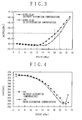
- Fig. 3 shows an actual measurement result of performance of the distortion compensating device in Fig. 1.
- a signal frequency is 900 MHz and a signal is of CDMA uplink with an Offset-QPSK modulated wave used and a diffusion rate set to 1.2288 Mcps.
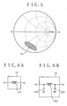
- Figs. 6A and 6B show concrete configuration examples of the first and second matching circuits 12 and 16 used in this actual measurement.
- the first matching circuit 12 can be composed of an inductor 121.
- the second matching circuit 16 can be composed of a type II circuit including capacitors 161 and 163 and an inductor 162.
- the configurations of the first and second matching circuits 12 and 16 in the present invention are not limited to ones shown in the figures.
- APR adjacent channel leakage power ratio
- a curve plotted with circle dots indicates a case without the distortion compensation
- a curve plotted with x dots indicates a case with the distortion compensation.
- Fig. 4 is a graph showing comparison in circuit power consumption between the case with the distortion of the present invention and the case without the distortion of the present invention.
- a curve plotted with circle dots similarly indicates the case without the distortion compensation and a curve plotted with x dots indicate the case with the distortion compensation.
- the current is increased by the operation of the FET 13, the operating current of the power amplifier 18 is reduced by the distortion compensation and thus, as a whole, it is apparent that the lower consumption of current is accomplished.
- Fig. 5 shows an appropriate range of the impedance Zs connected to the gate of the FET 13 in the present embodiment on a smith chart.
- the first embodiment is the distortion compensating device which is added to the existing power amplifier from the external, while the second embodiment is such that the distortion compensating function is added inside a power amplifier to be modularized.
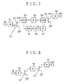
- Fig. 7 is a circuit block diagram showing a configuration example of a power amplifying device according to the second embodiment of the present invention.
- a configuration of a conventional typical power amplifier having no distortion compensating function is shown in Fig. 8.
- the power amplifier shown in Fig. 8 is a two-stage power amplifying circuit including two source grounded FETs, in which a first matching circuit 51, a first source grounded FET 52, a second matching circuit 53, a second source grounded FET 54 and a third matching circuit 55 are series-connected from an input terminal In to an output terminal OUT.
- This power amplifying device includes an input terminal IN, a first matching circuit 31, a first source grounded FET 32, a dividing circuit 33, a band pass filter (BPF) 35, an attenuation circuit (ATT) 36, a second matching circuit 37, a third matching circuit 34, an addition circuit (add) 38, a second source grounded FET 39, a fourth matching circuit 40 and an output terminal OUT.
- the matching circuit 31 is connected between a gate terminal of the source grounded FET 32 and the input terminal IN.
- the dividing circuit 33 is connected to a drain terminal of the FET 32 to divide the drain output into two.
- the band pass filter (BPF) 35 passing only a second harmonic and the attenuation circuit (ATT) 36 attenuating a signal voltage of the second harmonic are series-corrected to a first output terminal of the dividing circuit 33.
- the matching circuit 37 is connected between the attenuation circuit 36 and a first input terminal of the addition circuit 38.
- the matching circuit 34 is connected between a second output of the dividing circuit 33 and the addition circuit 38.
- the output of the adder 38 is connected to a gate of the second source grounded FET 39.
- the matching circuit 40 is connected between a drain of the FET 39 and the output terminal OUT.
- the matching circuit 31, FET 32, matching circuit 34 and FET 39 compose the main two-stage power amplifier.
- the dividing circuit 33, band pass filter 35, attenuation circuit 36, matching circuit 37 operate in the same manner as those of the first invention.
- An impedance Zs on the gate side of the FET 32 which is determined by the matching circuit 31 acts similarly to the impedance Zs in the first embodiment. More specifically, the phase of the second harmonic generated in the FET 32 is adjusted to be an optimal phase by setting the appropriate impedance Zs in the matching circuit 31. This can suppress the distortion generated in the FET 39.
- the FET 32 plays two roles of the first stage amplification of the main power amplifier and the generation of the second harmonic for suppressing the distortion generated in the final stage FET 39 of the main amplifier.
- a distortion component generated in the FET 32 also contributes to the distortion generated in the main amplifier, its amount is so small that it can be ignored as compared with the distortion generated in the FET 39, so that if the distortion generated in the FET 39 can be suppressed, the effect is sufficient.
- the FET can be replaced with a bipolar transistor.
- the terminals of the drain, source and gate of the FET correspond to the respective terminals of a collector, an emitter and a base of the bipolar transistor.
- a bias circuit or the like of the transistor is not shown in the figure, they can be added as necessary.
- the attenuation circuit and the matching circuit in the subsequent stage are deleted, an effect commensurate with the present invention can be attained.
Landscapes
- Physics & Mathematics (AREA)
- Nonlinear Science (AREA)
- Engineering & Computer Science (AREA)
- Power Engineering (AREA)
- Amplifiers (AREA)
- Transmitters (AREA)
Applications Claiming Priority (2)
| Application Number | Priority Date | Filing Date | Title |
|---|---|---|---|
| JP2004032351 | 2004-02-09 | ||
| JP2004032351A JP4868433B2 (ja) | 2004-02-09 | 2004-02-09 | 歪み補償装置および歪み補償機能付き電力増幅装置 |
Publications (3)
| Publication Number | Publication Date |
|---|---|
| EP1562286A2 true EP1562286A2 (fr) | 2005-08-10 |
| EP1562286A3 EP1562286A3 (fr) | 2008-03-05 |
| EP1562286B1 EP1562286B1 (fr) | 2011-07-20 |
Family
ID=34675592
Family Applications (1)
| Application Number | Title | Priority Date | Filing Date |
|---|---|---|---|
| EP05250604A Ceased EP1562286B1 (fr) | 2004-02-09 | 2005-02-03 | Dispositif pour la compensation des distorsions non-linéaires et amplificateur de puissance à fonction de compensation des distorsions |
Country Status (3)
| Country | Link |
|---|---|
| US (1) | US7259621B2 (fr) |
| EP (1) | EP1562286B1 (fr) |
| JP (1) | JP4868433B2 (fr) |
Cited By (1)
| Publication number | Priority date | Publication date | Assignee | Title |
|---|---|---|---|---|
| EP1898522A3 (fr) * | 2006-09-01 | 2009-04-01 | Sony Ericsson Mobile Communications Japan, Inc. | Système amplificateur de puissance et terminal de téléphone mobile l'utilisant |
Families Citing this family (32)
| Publication number | Priority date | Publication date | Assignee | Title |
|---|---|---|---|---|
| US6804502B2 (en) | 2001-10-10 | 2004-10-12 | Peregrine Semiconductor Corporation | Switch circuit and method of switching radio frequency signals |
| WO2006003959A1 (fr) * | 2004-06-30 | 2006-01-12 | Hitachi Metals, Ltd. | Circuit haute fréquence, composante haute fréquence, et appareil de communication multibande |
| US8081928B2 (en) * | 2005-02-03 | 2011-12-20 | Peregrine Semiconductor Corporation | Canceling harmonics in semiconductor RF switches |
| US7910993B2 (en) | 2005-07-11 | 2011-03-22 | Peregrine Semiconductor Corporation | Method and apparatus for use in improving linearity of MOSFET's using an accumulated charge sink |
| US8742502B2 (en) | 2005-07-11 | 2014-06-03 | Peregrine Semiconductor Corporation | Method and apparatus for use in improving linearity of MOSFETs using an accumulated charge sink-harmonic wrinkle reduction |
| US20080076371A1 (en) | 2005-07-11 | 2008-03-27 | Alexander Dribinsky | Circuit and method for controlling charge injection in radio frequency switches |
| US9653601B2 (en) | 2005-07-11 | 2017-05-16 | Peregrine Semiconductor Corporation | Method and apparatus for use in improving linearity of MOSFETs using an accumulated charge sink-harmonic wrinkle reduction |
| US7890891B2 (en) | 2005-07-11 | 2011-02-15 | Peregrine Semiconductor Corporation | Method and apparatus improving gate oxide reliability by controlling accumulated charge |
| USRE48965E1 (en) | 2005-07-11 | 2022-03-08 | Psemi Corporation | Method and apparatus improving gate oxide reliability by controlling accumulated charge |
| WO2007042850A1 (fr) | 2005-10-12 | 2007-04-19 | Acco | Transistor à effet de champ à grille isolé ayant une grille factice |
| KR100650685B1 (ko) | 2005-12-30 | 2006-11-30 | 엘지전자 주식회사 | Egprs용 전력증폭기 및 egprs용 전력증폭기의전력증폭방법 |
| US7750734B2 (en) * | 2007-03-23 | 2010-07-06 | Analog Devices, Inc. | Apparatus and methods for amplifiers |
| US7960772B2 (en) | 2007-04-26 | 2011-06-14 | Peregrine Semiconductor Corporation | Tuning capacitance to enhance FET stack voltage withstand |
| US7969243B2 (en) * | 2009-04-22 | 2011-06-28 | Acco Semiconductor, Inc. | Electronic circuits including a MOSFET and a dual-gate JFET |
| US8928410B2 (en) | 2008-02-13 | 2015-01-06 | Acco Semiconductor, Inc. | Electronic circuits including a MOSFET and a dual-gate JFET |
| US7863645B2 (en) * | 2008-02-13 | 2011-01-04 | ACCO Semiconductor Inc. | High breakdown voltage double-gate semiconductor device |
| US9240402B2 (en) | 2008-02-13 | 2016-01-19 | Acco Semiconductor, Inc. | Electronic circuits including a MOSFET and a dual-gate JFET |
| JPWO2010032283A1 (ja) * | 2008-09-16 | 2012-02-02 | 株式会社 Wave Technology | 高調波注入プッシュプル増幅器 |
| US7808415B1 (en) * | 2009-03-25 | 2010-10-05 | Acco Semiconductor, Inc. | Sigma-delta modulator including truncation and applications thereof |
| US7952431B2 (en) * | 2009-08-28 | 2011-05-31 | Acco Semiconductor, Inc. | Linearization circuits and methods for power amplification |
| US8532584B2 (en) | 2010-04-30 | 2013-09-10 | Acco Semiconductor, Inc. | RF switches |
| US9590674B2 (en) | 2012-12-14 | 2017-03-07 | Peregrine Semiconductor Corporation | Semiconductor devices with switchable ground-body connection |
| US20150236748A1 (en) | 2013-03-14 | 2015-08-20 | Peregrine Semiconductor Corporation | Devices and Methods for Duplexer Loss Reduction |
| US9406695B2 (en) | 2013-11-20 | 2016-08-02 | Peregrine Semiconductor Corporation | Circuit and method for improving ESD tolerance and switching speed |
| US9831857B2 (en) | 2015-03-11 | 2017-11-28 | Peregrine Semiconductor Corporation | Power splitter with programmable output phase shift |
| US9979361B1 (en) * | 2016-12-27 | 2018-05-22 | Nxp Usa, Inc. | Input circuits for RF amplifier devices, and methods of manufacture thereof |
| US10886911B2 (en) | 2018-03-28 | 2021-01-05 | Psemi Corporation | Stacked FET switch bias ladders |
| US10505530B2 (en) | 2018-03-28 | 2019-12-10 | Psemi Corporation | Positive logic switch with selectable DC blocking circuit |
| US10236872B1 (en) | 2018-03-28 | 2019-03-19 | Psemi Corporation | AC coupling modules for bias ladders |
| CN108649903B (zh) * | 2018-07-13 | 2024-12-24 | 成都四威功率电子科技有限公司 | 一种抑制倍频程功率放大器二次谐波的电路 |
| US11476849B2 (en) | 2020-01-06 | 2022-10-18 | Psemi Corporation | High power positive logic switch |
| CN113411062B (zh) * | 2021-08-19 | 2022-03-29 | 深圳飞骧科技股份有限公司 | 匹配电路、射频前端功率放大电路及移动通信设备 |
Citations (2)
| Publication number | Priority date | Publication date | Assignee | Title |
|---|---|---|---|---|
| US6249183B1 (en) | 1996-09-14 | 2001-06-19 | Daimlerchrysler Ag | High-efficiency amplifying device |
| US20030071684A1 (en) | 1999-12-17 | 2003-04-17 | Basim Noori | Linearisation method and signal processing device |
Family Cites Families (17)
| Publication number | Priority date | Publication date | Assignee | Title |
|---|---|---|---|---|
| JPS5573115A (en) * | 1978-11-27 | 1980-06-02 | Nec Corp | Traveling wave tube amplifying device |
| JPS59200504A (ja) * | 1983-04-26 | 1984-11-13 | Fujitsu Ltd | 逓倍器 |
| JPS62179205A (ja) * | 1986-02-03 | 1987-08-06 | Fujitsu Ltd | マイクロ波逓倍器 |
| JPS63114305A (ja) * | 1986-10-30 | 1988-05-19 | Fujitsu Ltd | 周波数逓倍器 |
| JP2807508B2 (ja) * | 1989-11-15 | 1998-10-08 | 株式会社エイ・ティ・アール光電波通信研究所 | マイクロ波周波数逓倍器 |
| IT1239472B (it) * | 1990-04-09 | 1993-11-02 | Sits Soc It Telecom Siemens | Linearizzatore del tipo a predistorsione per amplificatori di potenza a microonde |
| GB9502894D0 (en) * | 1995-02-15 | 1995-04-05 | British Tech Group | Amplifiers |
| JPH09107250A (ja) * | 1995-10-12 | 1997-04-22 | Sony Corp | 半導体増幅装置 |
| EP0827649A1 (fr) * | 1996-03-20 | 1998-03-11 | Koninklijke Philips Electronics N.V. | Circuit de preaccentuation pour signal analogique dans un reseau de videocommunication |
| JP3467670B2 (ja) * | 1996-07-26 | 2003-11-17 | 日本電信電話株式会社 | 歪補償回路 |
| JPH10126156A (ja) * | 1996-10-22 | 1998-05-15 | Japan Radio Co Ltd | 逓倍器 |
| JPH11289227A (ja) * | 1998-04-01 | 1999-10-19 | Nippon Telegr & Teleph Corp <Ntt> | 歪補償回路 |
| JP2001217659A (ja) * | 2000-02-03 | 2001-08-10 | Mitsubishi Electric Corp | マイクロ波増幅器 |
| JP2001223539A (ja) * | 2000-02-08 | 2001-08-17 | Nec Corp | アクティブフィードフォワード型プレディストーションに基づく線形電力増幅器 |
| JP3564382B2 (ja) * | 2000-10-24 | 2004-09-08 | 松下電器産業株式会社 | プリディストーション歪み補償回路 |
| JP2002368547A (ja) * | 2001-06-11 | 2002-12-20 | Hitachi Kokusai Electric Inc | 歪み改善回路 |
| JP3805221B2 (ja) * | 2001-09-18 | 2006-08-02 | 株式会社日立国際電気 | 歪み補償装置 |
-
2004
- 2004-02-09 JP JP2004032351A patent/JP4868433B2/ja not_active Expired - Fee Related
-
2005
- 2005-01-31 US US11/045,262 patent/US7259621B2/en not_active Expired - Fee Related
- 2005-02-03 EP EP05250604A patent/EP1562286B1/fr not_active Ceased
Patent Citations (2)
| Publication number | Priority date | Publication date | Assignee | Title |
|---|---|---|---|---|
| US6249183B1 (en) | 1996-09-14 | 2001-06-19 | Daimlerchrysler Ag | High-efficiency amplifying device |
| US20030071684A1 (en) | 1999-12-17 | 2003-04-17 | Basim Noori | Linearisation method and signal processing device |
Non-Patent Citations (1)
| Title |
|---|
| BUDIMIR D ET AL.: "Linearization of multichannel amplifiers with the injection of second harmonics into the amplifier and predistortion circuit", TELECOMMUNICATIONS IN MODERN SATELLITE, CABLE AND BROADCASTING SERVICE, vol. 1, 1 October 2003 (2003-10-01), pages 214 - 217 |
Cited By (2)
| Publication number | Priority date | Publication date | Assignee | Title |
|---|---|---|---|---|
| EP1898522A3 (fr) * | 2006-09-01 | 2009-04-01 | Sony Ericsson Mobile Communications Japan, Inc. | Système amplificateur de puissance et terminal de téléphone mobile l'utilisant |
| US7974597B2 (en) | 2006-09-01 | 2011-07-05 | Sony Ericsson Mobile Communications Japan, Inc. | Power amplifier system and mobile phone terminal using same |
Also Published As
| Publication number | Publication date |
|---|---|
| EP1562286A3 (fr) | 2008-03-05 |
| US7259621B2 (en) | 2007-08-21 |
| JP2005223849A (ja) | 2005-08-18 |
| EP1562286B1 (fr) | 2011-07-20 |
| JP4868433B2 (ja) | 2012-02-01 |
| US20050212595A1 (en) | 2005-09-29 |
Similar Documents
| Publication | Publication Date | Title |
|---|---|---|
| US7259621B2 (en) | Distortion compensating device and power amplifying device with distortion compensating function | |
| EP1620942B1 (fr) | Amplificateur rf a linearisation active de charge | |
| US9614480B2 (en) | Wide-band multi stage doherty power amplifier | |
| US7304537B2 (en) | Power amplification apparatus of a portable terminal | |
| EP2005577B1 (fr) | Commande de polarisation dynamique dans un amplificateur de puissance | |
| US20020039047A1 (en) | Power amplifier with gain change compensation | |
| US8718581B2 (en) | Method and apparatus for optimizing current consumption of amplifiers with power control | |
| US7307473B2 (en) | Distortion compensating and power amplifying apparatus | |
| KR20030090518A (ko) | 전력증폭장치와 그것을 이용한 무선통신장치 | |
| US8952758B2 (en) | Amplifier using nonlinear drivers | |
| US6522197B2 (en) | Method and apparatus for optimum biasing of cascaded MOSFET radio-frequency devices | |
| US6750724B1 (en) | Multistage amplifier | |
| US20090045878A1 (en) | Amplifier | |
| EP1667320A1 (fr) | Amplificateur | |
| US6313702B1 (en) | Phase correction amplifier and a feed-forward amplifier using the same | |
| KR100370545B1 (ko) | 고주파 선형 전력 증폭기의 대전력 방식 전치 왜곡 장치 | |
| Wood et al. | A high power, high efficiency UMTS amplifier using a novel Doherty configuration | |
| KR102912017B1 (ko) | 전력 증폭기용 rc 필터 기반의 적응형 선형화 회로 장치 | |
| EP1502352A2 (fr) | Appareil radio comprenant un amplificateur pour signaux de radiofrequence, amplificateur pour signaux de radiofrequence et procede pour amplifier ces signaux | |
| JP3393518B2 (ja) | モノリシック集積化低位相歪電力増幅器 | |
| KR100351657B1 (ko) | 다단 증폭단을 갖는 광대역 선형 증폭기 | |
| KR200252145Y1 (ko) | 광대역 전력 증폭기의 혼변조 성능 개선을 위해 다이오드믹서를 이용한 소형 프리디스토션 선형화기 | |
| Kim et al. | Linearity improvement of a power amplifier using a series LC resonant circuit |
Legal Events
| Date | Code | Title | Description |
|---|---|---|---|
| PUAI | Public reference made under article 153(3) epc to a published international application that has entered the european phase |
Free format text: ORIGINAL CODE: 0009012 |
|
| AK | Designated contracting states |
Kind code of ref document: A2 Designated state(s): AT BE BG CH CY CZ DE DK EE ES FI FR GB GR HU IE IS IT LI LT LU MC NL PL PT RO SE SI SK TR |
|
| AX | Request for extension of the european patent |
Extension state: AL BA HR LV MK YU |
|
| PUAL | Search report despatched |
Free format text: ORIGINAL CODE: 0009013 |
|
| AK | Designated contracting states |
Kind code of ref document: A3 Designated state(s): AT BE BG CH CY CZ DE DK EE ES FI FR GB GR HU IE IS IT LI LT LU MC NL PL PT RO SE SI SK TR |
|
| AX | Request for extension of the european patent |
Extension state: AL BA HR LV MK YU |
|
| 17P | Request for examination filed |
Effective date: 20080807 |
|
| 17Q | First examination report despatched |
Effective date: 20080910 |
|
| AKX | Designation fees paid |
Designated state(s): DE FR GB |
|
| GRAP | Despatch of communication of intention to grant a patent |
Free format text: ORIGINAL CODE: EPIDOSNIGR1 |
|
| GRAS | Grant fee paid |
Free format text: ORIGINAL CODE: EPIDOSNIGR3 |
|
| GRAA | (expected) grant |
Free format text: ORIGINAL CODE: 0009210 |
|
| AK | Designated contracting states |
Kind code of ref document: B1 Designated state(s): DE FR GB |
|
| REG | Reference to a national code |
Ref country code: DE Ref legal event code: R081 Ref document number: 602005029059 Country of ref document: DE Owner name: SNAPTRACK, INC., SAN DIEGO, US Free format text: FORMER OWNER: SONY ERICSSON MOBILE COMMUNICATIONS JAPAN, INC., TOKIO/TOKYO, JP Ref country code: DE Ref legal event code: R081 Ref document number: 602005029059 Country of ref document: DE Owner name: SONY MOBILE COMMUNICATIONS INC., JP Free format text: FORMER OWNER: SONY ERICSSON MOBILE COMMUNICATIONS JAPAN, INC., TOKIO/TOKYO, JP Ref country code: GB Ref legal event code: FG4D |
|
| REG | Reference to a national code |
Ref country code: DE Ref legal event code: R096 Ref document number: 602005029059 Country of ref document: DE Effective date: 20110908 |
|
| PLBE | No opposition filed within time limit |
Free format text: ORIGINAL CODE: 0009261 |
|
| STAA | Information on the status of an ep patent application or granted ep patent |
Free format text: STATUS: NO OPPOSITION FILED WITHIN TIME LIMIT |
|
| 26N | No opposition filed |
Effective date: 20120423 |
|
| REG | Reference to a national code |
Ref country code: DE Ref legal event code: R097 Ref document number: 602005029059 Country of ref document: DE Effective date: 20120423 |
|
| REG | Reference to a national code |
Ref country code: FR Ref legal event code: PLFP Year of fee payment: 11 |
|
| REG | Reference to a national code |
Ref country code: DE Ref legal event code: R082 Ref document number: 602005029059 Country of ref document: DE Representative=s name: FDST PATENTANWAELTE FREIER DOERR STAMMLER TSCH, DE Ref country code: DE Ref legal event code: R081 Ref document number: 602005029059 Country of ref document: DE Owner name: SNAPTRACK, INC., SAN DIEGO, US Free format text: FORMER OWNER: SONY ERICSSON MOBILE COMMUNICATIONS JAPAN, INC., TOKIO/TOKYO, JP Ref country code: DE Ref legal event code: R081 Ref document number: 602005029059 Country of ref document: DE Owner name: SONY MOBILE COMMUNICATIONS INC., JP Free format text: FORMER OWNER: SONY ERICSSON MOBILE COMMUNICATIONS JAPAN, INC., TOKIO/TOKYO, JP |
|
| REG | Reference to a national code |
Representative=s name: FDST PATENTANWAELTE FREIER DOERR STAMMLER TSCH, DE Ref country code: DE Ref legal event code: R082 Ref document number: 602005029059 Country of ref document: DE |
|
| REG | Reference to a national code |
Ref country code: FR Ref legal event code: CD Owner name: SONY MOBILE COMMUNICATIONS, INC Effective date: 20151209 |
|
| REG | Reference to a national code |
Ref country code: FR Ref legal event code: PLFP Year of fee payment: 12 |
|
| REG | Reference to a national code |
Ref country code: FR Ref legal event code: TP Owner name: SNAPTRACK, INC., US Effective date: 20161103 |
|
| REG | Reference to a national code |
Ref country code: FR Ref legal event code: PLFP Year of fee payment: 13 Ref country code: DE Ref legal event code: R081 Ref document number: 602005029059 Country of ref document: DE Owner name: SNAPTRACK, INC., SAN DIEGO, US Free format text: FORMER OWNER: SONY MOBILE COMMUNICATIONS INC., TOKYO, JP |
|
| REG | Reference to a national code |
Ref country code: GB Ref legal event code: 732E Free format text: REGISTERED BETWEEN 20161229 AND 20170104 |
|
| REG | Reference to a national code |
Ref country code: DE Ref legal event code: R082 Ref document number: 602005029059 Country of ref document: DE |
|
| REG | Reference to a national code |
Ref country code: FR Ref legal event code: PLFP Year of fee payment: 14 |
|
| PGFP | Annual fee paid to national office [announced via postgrant information from national office to epo] |
Ref country code: DE Payment date: 20180207 Year of fee payment: 14 Ref country code: GB Payment date: 20180125 Year of fee payment: 14 |
|
| PGFP | Annual fee paid to national office [announced via postgrant information from national office to epo] |
Ref country code: FR Payment date: 20180118 Year of fee payment: 14 |
|
| REG | Reference to a national code |
Ref country code: DE Ref legal event code: R119 Ref document number: 602005029059 Country of ref document: DE |
|
| GBPC | Gb: european patent ceased through non-payment of renewal fee |
Effective date: 20190203 |
|
| PG25 | Lapsed in a contracting state [announced via postgrant information from national office to epo] |
Ref country code: DE Free format text: LAPSE BECAUSE OF NON-PAYMENT OF DUE FEES Effective date: 20190903 Ref country code: GB Free format text: LAPSE BECAUSE OF NON-PAYMENT OF DUE FEES Effective date: 20190203 |
|
| PG25 | Lapsed in a contracting state [announced via postgrant information from national office to epo] |
Ref country code: FR Free format text: LAPSE BECAUSE OF NON-PAYMENT OF DUE FEES Effective date: 20190228 |