EP1564404A1 - Zündsystem für Kraftfahrzeuge mit funkloser sanfter Abschaltung als Thermisch-Überbelastungschutz - Google Patents
Zündsystem für Kraftfahrzeuge mit funkloser sanfter Abschaltung als Thermisch-Überbelastungschutz Download PDFInfo
- Publication number
- EP1564404A1 EP1564404A1 EP05075242A EP05075242A EP1564404A1 EP 1564404 A1 EP1564404 A1 EP 1564404A1 EP 05075242 A EP05075242 A EP 05075242A EP 05075242 A EP05075242 A EP 05075242A EP 1564404 A1 EP1564404 A1 EP 1564404A1
- Authority
- EP
- European Patent Office
- Prior art keywords
- switching device
- temperature
- control terminal
- current
- signal
- Prior art date
- Legal status (The legal status is an assumption and is not a legal conclusion. Google has not performed a legal analysis and makes no representation as to the accuracy of the status listed.)
- Granted
Links
Images


Classifications
-
- F—MECHANICAL ENGINEERING; LIGHTING; HEATING; WEAPONS; BLASTING
- F02—COMBUSTION ENGINES; HOT-GAS OR COMBUSTION-PRODUCT ENGINE PLANTS
- F02P—IGNITION, OTHER THAN COMPRESSION IGNITION, FOR INTERNAL-COMBUSTION ENGINES; TESTING OF IGNITION TIMING IN COMPRESSION-IGNITION ENGINES
- F02P3/00—Other installations
- F02P3/02—Other installations having inductive energy storage, e.g. arrangements of induction coils
- F02P3/04—Layout of circuits
- F02P3/055—Layout of circuits with protective means to prevent damage to the circuit, e.g. semiconductor devices or the ignition coil
-
- G—PHYSICS
- G01—MEASURING; TESTING
- G01K—MEASURING TEMPERATURE; MEASURING QUANTITY OF HEAT; THERMALLY-SENSITIVE ELEMENTS NOT OTHERWISE PROVIDED FOR
- G01K7/00—Measuring temperature based on the use of electric or magnetic elements directly sensitive to heat ; Power supply therefor, e.g. using thermoelectric elements
- G01K7/01—Measuring temperature based on the use of electric or magnetic elements directly sensitive to heat ; Power supply therefor, e.g. using thermoelectric elements using semiconducting elements having PN junctions
-
- F—MECHANICAL ENGINEERING; LIGHTING; HEATING; WEAPONS; BLASTING
- F02—COMBUSTION ENGINES; HOT-GAS OR COMBUSTION-PRODUCT ENGINE PLANTS
- F02D—CONTROLLING COMBUSTION ENGINES
- F02D41/00—Electrical control of supply of combustible mixture or its constituents
- F02D41/20—Output circuits, e.g. for controlling currents in command coils
- F02D2041/202—Output circuits, e.g. for controlling currents in command coils characterised by the control of the circuit
- F02D2041/2065—Output circuits, e.g. for controlling currents in command coils characterised by the control of the circuit the control being related to the coil temperature
-
- F—MECHANICAL ENGINEERING; LIGHTING; HEATING; WEAPONS; BLASTING
- F02—COMBUSTION ENGINES; HOT-GAS OR COMBUSTION-PRODUCT ENGINE PLANTS
- F02P—IGNITION, OTHER THAN COMPRESSION IGNITION, FOR INTERNAL-COMBUSTION ENGINES; TESTING OF IGNITION TIMING IN COMPRESSION-IGNITION ENGINES
- F02P3/00—Other installations
- F02P3/02—Other installations having inductive energy storage, e.g. arrangements of induction coils
- F02P3/04—Layout of circuits
- F02P3/045—Layout of circuits for control of the dwell or anti dwell time
- F02P3/0453—Opening or closing the primary coil circuit with semiconductor devices
-
- F—MECHANICAL ENGINEERING; LIGHTING; HEATING; WEAPONS; BLASTING
- F02—COMBUSTION ENGINES; HOT-GAS OR COMBUSTION-PRODUCT ENGINE PLANTS
- F02P—IGNITION, OTHER THAN COMPRESSION IGNITION, FOR INTERNAL-COMBUSTION ENGINES; TESTING OF IGNITION TIMING IN COMPRESSION-IGNITION ENGINES
- F02P9/00—Electric spark ignition control, not otherwise provided for
- F02P9/002—Control of spark intensity, intensifying, lengthening, suppression
Definitions
- the present invention is generally directed to an interface for providing thermal overload protection and, more specifically, to an automotive ignition system with sparkless thermal overload protection.
- Modem automotive ignition systems have provided protection from fault conditions that result in excessively long dwell times by a variety of techniques. For example, some systems have employed time-based protection that terminates a drive signal to an ignition coil current switching device, e.g., an insulated gate bipolar transistor (IGBT), when a predetermined dwell time was exceeded. Other existing systems have employed thermally triggered dwell termination that functions when excessively high temperatures are detected within a switching circuit and/or a control integrated circuit (IC). These methodologies, while generally effective in preventing damage to a control IC and/or a switching circuit, have several drawbacks. For example, time-based protection methods have required external timing capacitors.
- IGBT insulated gate bipolar transistor
- over-dwell protection systems have decreased an ignition coil current in a manner that has prevented the production of a spark at an associated spark plug. This type of sparkless dwell termination is commonly referred to as a "soft shutdown.”
- An example of one such over-dwell protection system is disclosed in U.S. Patent No. 5,819,713. This over-dwell protection system uses external timing capacitors to generate a slow ramp down voltage which is, in turn, applied to a control terminal of a switching device, e.g., a gate of an IGBT. While accomplishing the task of terminating a dwell event without the production of a spark, such systems incur the cost of an external capacitor, increased packaging space required for the capacitor and related interconnect wiring, as well as additional control die area for the required soft shutdown circuitry.
- Embodiments of the present invention are directed to an interface for providing thermal overload protection.
- the interface includes a switching device, a temperature indicating device, a drive circuit and a thermal monitoring circuit.
- the switching device includes a control terminal and a pair of output terminals that are configured to provide a drive current to an inductive load responsive to a control signal on the control terminal.
- the temperature indicating device is located approximate the switching device and receives a bias current and provides a temperature signal that provides an indication of a temperature of the switching device.
- the drive circuit is coupled to the control terminal of the switching device and provides the control signal at the control terminal of the switching device responsive to an external signal.
- the thermal monitoring circuit is coupled across the temperature indicating device and provides a shutdown signal to the drive circuit when the temperature of the switching device is above a predetermined temperature level, as indicated by the temperature signal.
- the drive circuit responds to the shutdown signal by removing current sources and current sinks from the control terminal of the switching device at which point leakage currents associated with the control terminal of the switching device cause the switching device to reduce the drive current to the inductive load in a predictable manner.
- a temperature of a switching device e.g., an insulated gate bipolar transistor (IGBT)
- IGBT insulated gate bipolar transistor
- IC control integrated circuit
- the control IC monitors a voltage developed across the diode string and if the voltage falls below a predetermined level, indicating a high temperature level, the drive connections to the control terminal of the switching device are effectively open circuited, allowing the switching device to, in effect, turn itself off via natural leakage currents associated with the control terminal.
- This turn-off period is sufficiently long so as to insure that current (i.e., ignition coil current) through the switching device is reduced at a rate that precludes a spark from occurring at an associated spark plug.
- an interface in response to a thermal overload condition, shuts off a gate drive to an insulated gate bipolar transistor (IGBT) in a fashion that reduces a coil current provided to a coil primary at a rate that prevents voltages on an associated coil secondary from reaching levels high enough to cause a spark across a gap of an associated spark plug.
- IGBT insulated gate bipolar transistor
- a diode string Ds integrated with a switching transistor 10, e.g., an IGBT, in a monolithic integrated circuit 20, includes a plurality of polysilicon diodes which are electrically isolated from active regions of the transistor 10.
- a current source I1 provides a bias current to the diode string Ds to develop a temperature-dependent voltage, which is monitored by a comparator C1, across the string Ds.
- the voltage across the diode string Ds decreases as the temperature of the transistor 10 increases, since the forward biased diode voltage has a negative temperature coefficient.
- an output of the comparator C1 changes state causing a latch (not separately shown in Fig. 1) in a soft shutdown control section 12 to be set.
- This latch records the fact that a thermal trip has occurred and is reset only when an electronic spark timing (EST) signal returns to an inactive state.
- a typical ignition system operates under what is known as a "ramp and hold" method of dwell timing.
- Engine control electronics issue an EST signal that is received by EST input circuitry 16.
- the transistor 10 is driven with a gate drive signal that forces the transistor 10 into saturation and the ignition coil 18 begins an inductively limited current charging period.
- a current limit control amplifier A1 acts to reduce the gate drive to a level that maintains a constant current through the coil 18 and transistor 10.
- the present invention when a thermal trip occurs, all transistors connected to the gate of the transistor 10 are turned off, removing any current sources or sinks, and causing the gate voltage to decay as a result of natural gate leakage currents associated with the transistor 10.
- This decay rate is sufficiently slow to allow a gradual decrease in coil current such that the coil energy dissipates without causing a high voltage spike at the coil secondary Ls output.
- the control circuitry may exist on a die separate from the transistor 10. However, due to the proximity of the control die to the transistor 10, the die temperature may be very high. At temperatures that may be as high as 160-185 degrees C, leakage currents inherent in junction isolated integrated circuitry become non-negligible. Therefore, any attempt to turn off the transistors coupled to the gate of the transistor 10, to allow a natural voltage decay to occur, will be disrupted by the junction leakage currents associated with any connected devices.
- a suitable technique for leakage current compensation is disclosed in U.S. Patent No. 6,369,646, which is hereby incorporated herein by reference in its entirety.
- This technique employs specific leakage compensator geometries that naturally track the current that leaks from epitaxial regions of NPN transistors to an adjacent substrate region. These compensators also automatically track silicon processing variations eliminating the need for trimming of the leakage compensator.
- By associating a leakage compensator with each epitaxial region connected to an IGBT gate an effective balance of currents can be achieved, allowing for slow gate voltage decay rates at virtually any temperature.
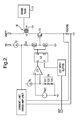
- Fig. 2 depicts a functional level schematic of one embodiment of the present invention.
- thermal diodes TD1-TD3, integrated with the transistor 10, provide a voltage input to an inverting input of the comparator C1.
- the non-inverting input of the comparator C1 receives a reference voltage Vref that is selected, based on known thermal characteristics of the thermal diodes TD1-TD3.
- Vref reference voltage
- the diodes TD1-TD3 reach a thermal trip temperature, their combined forward voltage drop, as established by current source I1, falls below Vref which causes an output of the comparator C1 to transition to a high state.
- the output of the comparator C1 is coupled to a SET input of latch L1.
- the latch L1 When the output of the comparator C1 transitions to the high state, an output Q of the latch L1 goes high effectively opening all connections to the gate terminal of the transistor 10.
- the latch L1 may be reset directly by a low level (non-fault) input at the EST input. Alternatively, completion of the soft shutdown cycle may be required before allowing the transistor 10 to be turned on again. This generally precludes the possibility of generating a mistimed spark due to the fall of EST during the soft shutdown period.
- the current limit function operates independently of the invention circuitry and is also disconnected from the transistor 10 gate during (and after) the soft-shutdown event.
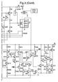
- Fig. 3 shows a transistor level schematic of one embodiment of the present invention.
- Transistors Q9-Q18 and resistors R9-R14 compose a reference current generator of the type generally known as a "Delta Vbe" generator.
- This type of current generator is a standard building block, which is known to those, skilled in the art and, as such, is not further described herein.
- kT/q k is Boltzman's constant, T is the temperature in degrees Kelvin and q is the electric charge.
- N is set equal to 9.
- the reference current Iref is used to bias a current mirror rail that biases other circuitry including the circuitry that establishes the gate drive output charging current. This output current is developed by mirroring a copy of Iref, sourced by the collector of transistor Q1, via the NPN current mirror composed of transistors Q2 and Q4 along with resistors R2 and R4, onto transistor Q5.
- the transistor Q5 is in turn part of a PNP current mirror composed of transistors Q6 and Q7 and resistors R3, R5, and R6.
- the collector current of the transistor Q7 is the charging current used for turning on IGBT 10.
- Transistor Q3, driven by the EST input circuitry acts as a switch to enable or disable the gate drive output current. When the EST signal commands the IGBT 10 into the off state, transistor Q3 is turned on which disables the transistors Q2 and Q4 and enables the transistor Q8, pulling the gate of the IGBT 10 low.
- the current limit control circuitry which is an error amplifier with negative feedback, is composed of transistors Q100-Q105 and resistors RITRIM and R100-R105. This circuitry responds to the IGBT 10 emitter current via a voltage sensed across the sense resistor Rsense.
- the current limit control circuitry controls the voltage applied to the gate of the IGBT 10 in order to establish a stable, limited IGBT 10 current.
- Resistor R7 acts to aid in the stability of this control loop.
- a feedback resistor Rfb provides local feedback and, in part, sets the gain of the current limit control loop.
- the output section of this amplifier, composed of the transistors Q104-Q105 and the resistors R104-R105 can be effectively disconnected from its ground connection by turning off transistor Q224. Removing this current sinking path is part of the process of isolating the IGBT 10 gate from any current sources or sinks during the soft shutdown period.
- transistors Q101 and Q103 are turned off by transistor Q222 to prevent the transistor Q103 from pulling current away from the IGBT 10 gate.
- the transistor Q102 pulls the connected end of the resistor Rfb high, reverse biasing diode connected transistor QD 1.
- Transistor Q221 turns off the NPN current mirror combination of the transistors Q2 and Q4. This in turn shuts off the PNP current mirror made up of the transistors Q5 and Q7.
- Resistor R5 acts to pull up the bases of these two transistors, ensuring that the transistor Q7 does not source any current onto the gate of the IGBT 10.
- transistor Q8 already being commanded off by the EST input, all paths for current flowing to or from the IGBT 10 gate have been deactivated. The signals that control this deactivation, based on the IGBT 10 temperature, are further discussed below.
- a relatively temperature independent reference voltage can be developed by forcing the delta Vbe current through a series combination of one or more diodes and a carefully selected integrated silicon diffused resistor. Silicon diffused resistors typically have positive temperature coefficients, while the integrated diode forward voltage drops have a negative temperature coefficient.
- a voltage that is some multiple of the silicon bandgap voltage (approximately 1.26 volts) is developed.
- a "Vbe multiplier" configuration may be used in place of a fixed number of individual diodes.
- Transistor Q215 combined with resistors R205 and R206, forms the Vbe multiplier. The voltage across the collector and emitter terminals of the transistor Q215 is defined by: Vbe(1+R205/R206)
- This voltage is in series with the voltage drop formed across the resistor Rref and the trim resistor Rtrim.
- the reference voltage Vref is transferred to the diode tied transistor Q211, via the biased base-emitter junctions of transistors Q214 and Q210.
- the voltage across a base-emitter junction of the transistor Q211 is used to offset one Vbe voltage component of the voltage developed across the collector and emitter of the transistor Q215. This allows a reference voltage with a magnitude less than one silicon bandgap voltage to be applied to the thermal diode string.
- the overall thermal regulation point can be modified as desired for a given application.
- the thermal reference voltage is compared to the voltage present across the string of thermal sense diodes TD1-TD3 integrated with the IGBT 10.
- the diodes TD1-TD3 are biased by the current from transistor Q200, both directly and via a diode tied transistor Q201.
- Transistors Q203-209 and resistor R202 form a comparator.
- the output of the comparator, at the collector of transistor Q207, drives both transistors Q217 and Q202.
- the transistor Q202 acts to shunt some of bias current of the transistor Q200 to ground, when a thermal trip has occurred. This action serves to provide a hysteresis function in the thermal comparator, causing its output to remain high for an extended period of time.
- the transistor Q217 is part of a simple SR latch composed of transistors Q217-Q220 and resistors R208-R211.
- the latch When a thermal trip occurs, as detected by the comparator, the latch is set, causing the voltage at the collector of the transistor Q220 to assume a high state. This high level logic signal then drives transistors Q221-Q224.
- These transistors as described above, handle the isolation of the IGBT 10 gate, allowing the soft shutdown to proceed.
- the latch is reset by the inverted output of the EST input circuitry, when the EST signal transitions to a low level.
- the compensation for the leakage currents in the epitaxial pockets associated with transistors connected to the IGBT 10 gate may be handled by the device Qleak1, represented by a multiple collector PNP transistor.
- This device may be scaled, as described in U.S. Patent No. 6,369,646, to provide an equal balance for the epitaxial region to isolation leakage currents inherent to the devices that are attached to the IGBT 10 gate.
- circuitry has been described herein that performs temperature-based over-dwell termination and provides a soft shutdown without requiring external timing or soft shutdown control capacitors. Such circuitry may advantageously be employed within an automotive ignition system.
Landscapes
- Engineering & Computer Science (AREA)
- Physics & Mathematics (AREA)
- General Physics & Mathematics (AREA)
- Chemical & Material Sciences (AREA)
- Combustion & Propulsion (AREA)
- Mechanical Engineering (AREA)
- General Engineering & Computer Science (AREA)
- Electronic Switches (AREA)
- Protection Of Generators And Motors (AREA)
- Control Of Eletrric Generators (AREA)
- Control Of Electric Motors In General (AREA)
Applications Claiming Priority (2)
| Application Number | Priority Date | Filing Date | Title |
|---|---|---|---|
| US779906 | 2004-02-17 | ||
| US10/779,906 US6955164B2 (en) | 2004-02-17 | 2004-02-17 | Automotive ignition system with sparkless thermal overload protection |
Publications (2)
| Publication Number | Publication Date |
|---|---|
| EP1564404A1 true EP1564404A1 (de) | 2005-08-17 |
| EP1564404B1 EP1564404B1 (de) | 2009-11-25 |
Family
ID=34701431
Family Applications (1)
| Application Number | Title | Priority Date | Filing Date |
|---|---|---|---|
| EP05075242A Expired - Lifetime EP1564404B1 (de) | 2004-02-17 | 2005-01-31 | Zündsystem für Kraftfahrzeuge mit funkloser sanfter Abschaltung als Thermisch-Überbelastungschutz |
Country Status (4)
| Country | Link |
|---|---|
| US (1) | US6955164B2 (de) |
| EP (1) | EP1564404B1 (de) |
| AT (1) | ATE449907T1 (de) |
| DE (1) | DE602005017838D1 (de) |
Cited By (4)
| Publication number | Priority date | Publication date | Assignee | Title |
|---|---|---|---|---|
| EP1898390A1 (de) * | 2006-09-11 | 2008-03-12 | Samsung SDI Co., Ltd. | Plasmaanzeige und Spannungsgenerator dafür |
| CN101786423A (zh) * | 2010-03-11 | 2010-07-28 | 武汉蓝星科技股份有限公司 | 一种车载信息系统开关机保护电路 |
| US7857509B2 (en) | 2007-08-22 | 2010-12-28 | Gm Global Technology Operations, Inc. | Temperature sensing arrangements for power electronic devices |
| CN110778437A (zh) * | 2018-07-25 | 2020-02-11 | 半导体元件工业有限责任公司 | 用于线圈的软关断的电路和方法 |
Families Citing this family (31)
| Publication number | Priority date | Publication date | Assignee | Title |
|---|---|---|---|---|
| US7304905B2 (en) | 2004-05-24 | 2007-12-04 | Intel Corporation | Throttling memory in response to an internal temperature of a memory device |
| US7523285B2 (en) * | 2004-08-20 | 2009-04-21 | Intel Corporation | Thermal memory control |
| JP2010014445A (ja) * | 2008-07-01 | 2010-01-21 | Seiko Instruments Inc | 半導体温度センサ |
| JP5423378B2 (ja) * | 2009-12-15 | 2014-02-19 | 三菱電機株式会社 | イグナイタ用電力半導体装置 |
| JP5031081B2 (ja) * | 2010-10-12 | 2012-09-19 | 三菱電機株式会社 | 内燃機関用電子制御装置 |
| WO2013067538A1 (en) | 2011-11-04 | 2013-05-10 | Nevro Corporation | Medical device communication and charding assemblies for use with implantable signal generators |
| JP6013059B2 (ja) * | 2012-07-20 | 2016-10-25 | ローム株式会社 | スイッチ制御回路、イグナイタ、エンジン点火装置、車両 |
| AU2014259681B2 (en) | 2013-05-03 | 2018-08-09 | Nevro Corporation | Molded headers for implantable signal generators, and associated systems and methods |
| WO2015084410A1 (en) * | 2013-12-06 | 2015-06-11 | Intel Corporation | Method and apparatus for calibrating a sensor |
| AU2015264561B2 (en) | 2014-05-20 | 2020-02-20 | Nevro Corporation | Implanted pulse generators with reduced power consumption via signal strength/duration characteristics, and associated systems and methods |
| US9884198B2 (en) | 2014-10-22 | 2018-02-06 | Nevro Corp. | Systems and methods for extending the life of an implanted pulse generator battery |
| US9517344B1 (en) | 2015-03-13 | 2016-12-13 | Nevro Corporation | Systems and methods for selecting low-power, effective signal delivery parameters for an implanted pulse generator |
| DE102015213831A1 (de) * | 2015-07-22 | 2017-01-26 | Robert Bosch Gmbh | Verfahren zum Außer-Betrieb-Setzen einer elektrisch angesteuerten Komponente eines Fahrzeugs in einem Fehlerfall einer die Komponente ansteuernden Recheneinheit |
| KR101856335B1 (ko) * | 2016-06-30 | 2018-05-09 | 현대자동차주식회사 | 다이오드 온도 감지의 자동 보정이 가능한 igbt 온도 감지 회로 |
| JP6696334B2 (ja) * | 2016-07-11 | 2020-05-20 | 株式会社デンソー | 点火装置 |
| DE112018000426B4 (de) * | 2017-03-01 | 2024-10-24 | Hitachi Astemo, Ltd. | Zündsteuervorrichtung und Referenzspannungs-Einstellverfahren der Zündsteuervorrichtung |
| KR102388147B1 (ko) * | 2017-05-08 | 2022-04-19 | 현대자동차주식회사 | Igbt 온도 센서 보정 장치 및 이를 이용한 온도센싱 보정 방법 |
| US11128110B2 (en) | 2017-12-18 | 2021-09-21 | Semiconductor Components Industries, Llc | Methods and apparatus for an ignition system |
| JP7056160B2 (ja) * | 2018-01-16 | 2022-04-19 | 株式会社デンソー | 内燃機関の点火装置 |
| AU2019214966B2 (en) | 2018-01-30 | 2024-12-05 | Nevro Corp. | Efficient use of an implantable pulse generator battery, and associated systems and methods |
| JP7143398B2 (ja) * | 2018-03-13 | 2022-09-28 | ローム株式会社 | スイッチ制御回路、イグナイタ |
| US11131286B2 (en) * | 2018-03-20 | 2021-09-28 | Rohm Co., Ltd. | Igniter and vehicle provided with the same |
| JP7125020B2 (ja) * | 2018-03-20 | 2022-08-24 | ローム株式会社 | イグナイタ、および、当該イグナイタを備える車両 |
| SE542389C2 (en) * | 2018-09-04 | 2020-04-21 | Sem Ab | An ignition system and method controlling spark ignited combustion engines |
| US10975827B2 (en) | 2018-09-26 | 2021-04-13 | Semiconductor Components Industries, Llc | Ignition control system with circulating-current control |
| EP3917612A4 (de) * | 2019-01-31 | 2022-08-31 | Nevro Corp. | Leistungssteuerschaltung für sterilisierte geräte und zugehörige systeme und verfahren |
| US10933238B2 (en) | 2019-01-31 | 2021-03-02 | Nevro Corp. | Power control circuit for sterilized devices, and associated systems and methods |
| US11274645B2 (en) * | 2019-10-15 | 2022-03-15 | Semiconductor Components Industries, Llc | Circuit and method for a kickback-limited soft shutdown of a coil |
| CN115298943A (zh) * | 2020-03-24 | 2022-11-04 | 三菱电机株式会社 | 半导体驱动装置、半导体装置以及电力变换装置 |
| JP7419948B2 (ja) * | 2020-04-16 | 2024-01-23 | 株式会社デンソー | 内燃機関の点火装置 |
| CN117277773B (zh) * | 2023-09-27 | 2024-08-30 | 成都智融微电子有限公司 | 保护方法、保护装置、开关电源和计算机可读存储介质 |
Citations (6)
| Publication number | Priority date | Publication date | Assignee | Title |
|---|---|---|---|---|
| EP0256715A2 (de) * | 1986-08-18 | 1988-02-24 | Siliconix Limited | Temperaturfühlvorrichtung |
| EP0846858A1 (de) * | 1996-12-09 | 1998-06-10 | Delco Electronics Corporation | Zündsteuerungssystem für Kraftfahrzeuge |
| WO2001025625A1 (de) * | 1999-10-06 | 2001-04-12 | Robert Bosch Gmbh | Vorrichtung und verfahren zur zündung einer brennkraftmaschine |
| US6360720B1 (en) * | 2000-07-24 | 2002-03-26 | Delphi Technologies, Inc. | High temperature compensation circuitry for an ignition control circuit |
| WO2003034590A1 (de) * | 2001-10-09 | 2003-04-24 | Robert Bosch Gmbh | Halbleiter-schaltungsanordnung, insbesondere für zündungsverwendungen, und verwendung |
| US20040011342A1 (en) * | 2002-07-02 | 2004-01-22 | Hitachi, Ltd. | Electronic device for internal combustion engine such as ignition device |
Family Cites Families (7)
| Publication number | Priority date | Publication date | Assignee | Title |
|---|---|---|---|---|
| US6100728A (en) * | 1995-07-31 | 2000-08-08 | Delco Electronics Corp. | Coil current limiting feature for an ignition coil driver module |
| JPH10338350A (ja) * | 1997-06-11 | 1998-12-22 | Toyo Kanetsu Kk | ケース積み付け設備 |
| JP3484123B2 (ja) * | 2000-01-12 | 2004-01-06 | 株式会社日立製作所 | 内燃機関用点火装置 |
| AU2001238675A1 (en) * | 2000-02-23 | 2001-09-03 | Sri International | Electroactive polymer thermal electric generators |
| US6450157B1 (en) * | 2000-07-03 | 2002-09-17 | Delphi Technologies, Inc. | Automotive ignition system with adaptable start-of-dwell ring damping |
| US6369646B1 (en) * | 2001-01-29 | 2002-04-09 | Delphi Technologies, Inc. | Leakage current compensation circuit |
| US6777781B1 (en) * | 2003-04-14 | 2004-08-17 | National Semiconductor Corporation | Base-to-substrate leakage cancellation |
-
2004
- 2004-02-17 US US10/779,906 patent/US6955164B2/en not_active Expired - Lifetime
-
2005
- 2005-01-31 EP EP05075242A patent/EP1564404B1/de not_active Expired - Lifetime
- 2005-01-31 AT AT05075242T patent/ATE449907T1/de not_active IP Right Cessation
- 2005-01-31 DE DE602005017838T patent/DE602005017838D1/de not_active Expired - Lifetime
Patent Citations (6)
| Publication number | Priority date | Publication date | Assignee | Title |
|---|---|---|---|---|
| EP0256715A2 (de) * | 1986-08-18 | 1988-02-24 | Siliconix Limited | Temperaturfühlvorrichtung |
| EP0846858A1 (de) * | 1996-12-09 | 1998-06-10 | Delco Electronics Corporation | Zündsteuerungssystem für Kraftfahrzeuge |
| WO2001025625A1 (de) * | 1999-10-06 | 2001-04-12 | Robert Bosch Gmbh | Vorrichtung und verfahren zur zündung einer brennkraftmaschine |
| US6360720B1 (en) * | 2000-07-24 | 2002-03-26 | Delphi Technologies, Inc. | High temperature compensation circuitry for an ignition control circuit |
| WO2003034590A1 (de) * | 2001-10-09 | 2003-04-24 | Robert Bosch Gmbh | Halbleiter-schaltungsanordnung, insbesondere für zündungsverwendungen, und verwendung |
| US20040011342A1 (en) * | 2002-07-02 | 2004-01-22 | Hitachi, Ltd. | Electronic device for internal combustion engine such as ignition device |
Cited By (6)
| Publication number | Priority date | Publication date | Assignee | Title |
|---|---|---|---|---|
| EP1898390A1 (de) * | 2006-09-11 | 2008-03-12 | Samsung SDI Co., Ltd. | Plasmaanzeige und Spannungsgenerator dafür |
| US7857509B2 (en) | 2007-08-22 | 2010-12-28 | Gm Global Technology Operations, Inc. | Temperature sensing arrangements for power electronic devices |
| CN101786423A (zh) * | 2010-03-11 | 2010-07-28 | 武汉蓝星科技股份有限公司 | 一种车载信息系统开关机保护电路 |
| CN101786423B (zh) * | 2010-03-11 | 2012-01-04 | 武汉蓝星科技股份有限公司 | 一种车载信息系统开关机保护电路 |
| CN110778437A (zh) * | 2018-07-25 | 2020-02-11 | 半导体元件工业有限责任公司 | 用于线圈的软关断的电路和方法 |
| CN110778437B (zh) * | 2018-07-25 | 2021-10-29 | 半导体元件工业有限责任公司 | 用于线圈的软关断的电路和方法 |
Also Published As
| Publication number | Publication date |
|---|---|
| US6955164B2 (en) | 2005-10-18 |
| US20050178372A1 (en) | 2005-08-18 |
| DE602005017838D1 (de) | 2010-01-07 |
| EP1564404B1 (de) | 2009-11-25 |
| ATE449907T1 (de) | 2009-12-15 |
Similar Documents
| Publication | Publication Date | Title |
|---|---|---|
| EP1564404B1 (de) | Zündsystem für Kraftfahrzeuge mit funkloser sanfter Abschaltung als Thermisch-Überbelastungschutz | |
| US6987655B2 (en) | Thermal overload protection circuit for an automotive ignition system | |
| US20070086807A1 (en) | Image forming apparatus with detachable power-requiring unit | |
| EP0067435B1 (de) | Pulsbreitesteuerungskreis, in dem das Mass der Rückkupplung abhängig von der Arbeitstemperatur ist | |
| TWI509925B (zh) | Module for protecting power conversion system and method and system controller thereof | |
| US6539929B2 (en) | Ignition device for an internal combustion engine | |
| EP0757177B1 (de) | Zündsystem für Brennkraftmaschine | |
| CN1917321B (zh) | 热保护电路、功率传输集成电路及功率传输方法 | |
| US6735064B2 (en) | Inrush current suppressing device | |
| US4092693A (en) | Temperature sensing protection circuit for ic power chip having thermal hysteresis characteristic | |
| CN101123356A (zh) | 充电和放电控制电路以及充电型电源装置 | |
| US6330143B1 (en) | Automatic over-current protection of transistors | |
| US7095182B2 (en) | Ignition control apparatus for internal combustion engine | |
| US6597556B1 (en) | Circuit for protection from excess temperature | |
| US8665004B2 (en) | Controlling a MOS transistor | |
| US4962300A (en) | Preheating control apparatus for diesel engines | |
| US5796280A (en) | Thermal limit circuit with built-in hysteresis | |
| US6668811B1 (en) | Ignition control circuit providing temperature and battery voltage compensated coil current control | |
| EP0359851B1 (de) | Zündanlage für Innenverbrennungsmaschinen | |
| US6360720B1 (en) | High temperature compensation circuitry for an ignition control circuit | |
| JPH08338350A (ja) | 内燃機関用点火装置 | |
| US20030179033A1 (en) | Control of a power load | |
| KR20010006039A (ko) | 소비 장치에 공급되는 전류를 조절하기 위한 장치 | |
| US6545478B2 (en) | Electronic ignition device for an engine | |
| US6798176B2 (en) | Alternator for a motor vehicle with energizing information output |
Legal Events
| Date | Code | Title | Description |
|---|---|---|---|
| PUAI | Public reference made under article 153(3) epc to a published international application that has entered the european phase |
Free format text: ORIGINAL CODE: 0009012 |
|
| AK | Designated contracting states |
Kind code of ref document: A1 Designated state(s): AT BE BG CH CY CZ DE DK EE ES FI FR GB GR HU IE IS IT LI LT LU MC NL PL PT RO SE SI SK TR |
|
| AX | Request for extension of the european patent |
Extension state: AL BA HR LV MK YU |
|
| 17P | Request for examination filed |
Effective date: 20060217 |
|
| AKX | Designation fees paid |
Designated state(s): AT BE BG CH CY CZ DE DK EE ES FI FR GB GR HU IE IS IT LI LT LU MC NL PL PT RO SE SI SK TR |
|
| 17Q | First examination report despatched |
Effective date: 20061129 |
|
| GRAP | Despatch of communication of intention to grant a patent |
Free format text: ORIGINAL CODE: EPIDOSNIGR1 |
|
| GRAS | Grant fee paid |
Free format text: ORIGINAL CODE: EPIDOSNIGR3 |
|
| GRAA | (expected) grant |
Free format text: ORIGINAL CODE: 0009210 |
|
| AK | Designated contracting states |
Kind code of ref document: B1 Designated state(s): AT BE BG CH CY CZ DE DK EE ES FI FR GB GR HU IE IS IT LI LT LU MC NL PL PT RO SE SI SK TR |
|
| REG | Reference to a national code |
Ref country code: GB Ref legal event code: FG4D |
|
| REG | Reference to a national code |
Ref country code: CH Ref legal event code: EP |
|
| REG | Reference to a national code |
Ref country code: IE Ref legal event code: FG4D |
|
| REF | Corresponds to: |
Ref document number: 602005017838 Country of ref document: DE Date of ref document: 20100107 Kind code of ref document: P |
|
| REG | Reference to a national code |
Ref country code: NL Ref legal event code: VDEP Effective date: 20091125 |
|
| LTIE | Lt: invalidation of european patent or patent extension |
Effective date: 20091125 |
|
| PG25 | Lapsed in a contracting state [announced via postgrant information from national office to epo] |
Ref country code: LT Free format text: LAPSE BECAUSE OF FAILURE TO SUBMIT A TRANSLATION OF THE DESCRIPTION OR TO PAY THE FEE WITHIN THE PRESCRIBED TIME-LIMIT Effective date: 20091125 Ref country code: IS Free format text: LAPSE BECAUSE OF FAILURE TO SUBMIT A TRANSLATION OF THE DESCRIPTION OR TO PAY THE FEE WITHIN THE PRESCRIBED TIME-LIMIT Effective date: 20100325 Ref country code: FI Free format text: LAPSE BECAUSE OF FAILURE TO SUBMIT A TRANSLATION OF THE DESCRIPTION OR TO PAY THE FEE WITHIN THE PRESCRIBED TIME-LIMIT Effective date: 20091125 Ref country code: PT Free format text: LAPSE BECAUSE OF FAILURE TO SUBMIT A TRANSLATION OF THE DESCRIPTION OR TO PAY THE FEE WITHIN THE PRESCRIBED TIME-LIMIT Effective date: 20100325 Ref country code: SE Free format text: LAPSE BECAUSE OF FAILURE TO SUBMIT A TRANSLATION OF THE DESCRIPTION OR TO PAY THE FEE WITHIN THE PRESCRIBED TIME-LIMIT Effective date: 20091125 |
|
| PG25 | Lapsed in a contracting state [announced via postgrant information from national office to epo] |
Ref country code: PL Free format text: LAPSE BECAUSE OF FAILURE TO SUBMIT A TRANSLATION OF THE DESCRIPTION OR TO PAY THE FEE WITHIN THE PRESCRIBED TIME-LIMIT Effective date: 20091125 Ref country code: CY Free format text: LAPSE BECAUSE OF FAILURE TO SUBMIT A TRANSLATION OF THE DESCRIPTION OR TO PAY THE FEE WITHIN THE PRESCRIBED TIME-LIMIT Effective date: 20091125 Ref country code: SI Free format text: LAPSE BECAUSE OF FAILURE TO SUBMIT A TRANSLATION OF THE DESCRIPTION OR TO PAY THE FEE WITHIN THE PRESCRIBED TIME-LIMIT Effective date: 20091125 |
|
| PG25 | Lapsed in a contracting state [announced via postgrant information from national office to epo] |
Ref country code: BE Free format text: LAPSE BECAUSE OF FAILURE TO SUBMIT A TRANSLATION OF THE DESCRIPTION OR TO PAY THE FEE WITHIN THE PRESCRIBED TIME-LIMIT Effective date: 20091125 Ref country code: AT Free format text: LAPSE BECAUSE OF FAILURE TO SUBMIT A TRANSLATION OF THE DESCRIPTION OR TO PAY THE FEE WITHIN THE PRESCRIBED TIME-LIMIT Effective date: 20091125 |
|
| PG25 | Lapsed in a contracting state [announced via postgrant information from national office to epo] |
Ref country code: RO Free format text: LAPSE BECAUSE OF FAILURE TO SUBMIT A TRANSLATION OF THE DESCRIPTION OR TO PAY THE FEE WITHIN THE PRESCRIBED TIME-LIMIT Effective date: 20091125 Ref country code: BG Free format text: LAPSE BECAUSE OF FAILURE TO SUBMIT A TRANSLATION OF THE DESCRIPTION OR TO PAY THE FEE WITHIN THE PRESCRIBED TIME-LIMIT Effective date: 20100225 Ref country code: DK Free format text: LAPSE BECAUSE OF FAILURE TO SUBMIT A TRANSLATION OF THE DESCRIPTION OR TO PAY THE FEE WITHIN THE PRESCRIBED TIME-LIMIT Effective date: 20091125 Ref country code: EE Free format text: LAPSE BECAUSE OF FAILURE TO SUBMIT A TRANSLATION OF THE DESCRIPTION OR TO PAY THE FEE WITHIN THE PRESCRIBED TIME-LIMIT Effective date: 20091125 Ref country code: ES Free format text: LAPSE BECAUSE OF FAILURE TO SUBMIT A TRANSLATION OF THE DESCRIPTION OR TO PAY THE FEE WITHIN THE PRESCRIBED TIME-LIMIT Effective date: 20100308 Ref country code: NL Free format text: LAPSE BECAUSE OF FAILURE TO SUBMIT A TRANSLATION OF THE DESCRIPTION OR TO PAY THE FEE WITHIN THE PRESCRIBED TIME-LIMIT Effective date: 20091125 |
|
| PG25 | Lapsed in a contracting state [announced via postgrant information from national office to epo] |
Ref country code: CZ Free format text: LAPSE BECAUSE OF FAILURE TO SUBMIT A TRANSLATION OF THE DESCRIPTION OR TO PAY THE FEE WITHIN THE PRESCRIBED TIME-LIMIT Effective date: 20091125 Ref country code: MC Free format text: LAPSE BECAUSE OF NON-PAYMENT OF DUE FEES Effective date: 20100131 Ref country code: SK Free format text: LAPSE BECAUSE OF FAILURE TO SUBMIT A TRANSLATION OF THE DESCRIPTION OR TO PAY THE FEE WITHIN THE PRESCRIBED TIME-LIMIT Effective date: 20091125 |
|
| REG | Reference to a national code |
Ref country code: CH Ref legal event code: PL |
|
| PLBE | No opposition filed within time limit |
Free format text: ORIGINAL CODE: 0009261 |
|
| STAA | Information on the status of an ep patent application or granted ep patent |
Free format text: STATUS: NO OPPOSITION FILED WITHIN TIME LIMIT |
|
| PG25 | Lapsed in a contracting state [announced via postgrant information from national office to epo] |
Ref country code: CH Free format text: LAPSE BECAUSE OF NON-PAYMENT OF DUE FEES Effective date: 20100131 Ref country code: GR Free format text: LAPSE BECAUSE OF FAILURE TO SUBMIT A TRANSLATION OF THE DESCRIPTION OR TO PAY THE FEE WITHIN THE PRESCRIBED TIME-LIMIT Effective date: 20100226 Ref country code: LI Free format text: LAPSE BECAUSE OF NON-PAYMENT OF DUE FEES Effective date: 20100131 |
|
| 26N | No opposition filed |
Effective date: 20100826 |
|
| PG25 | Lapsed in a contracting state [announced via postgrant information from national office to epo] |
Ref country code: IE Free format text: LAPSE BECAUSE OF NON-PAYMENT OF DUE FEES Effective date: 20100131 |
|
| PG25 | Lapsed in a contracting state [announced via postgrant information from national office to epo] |
Ref country code: IT Free format text: LAPSE BECAUSE OF FAILURE TO SUBMIT A TRANSLATION OF THE DESCRIPTION OR TO PAY THE FEE WITHIN THE PRESCRIBED TIME-LIMIT Effective date: 20091125 |
|
| PG25 | Lapsed in a contracting state [announced via postgrant information from national office to epo] |
Ref country code: LU Free format text: LAPSE BECAUSE OF NON-PAYMENT OF DUE FEES Effective date: 20100131 Ref country code: HU Free format text: LAPSE BECAUSE OF FAILURE TO SUBMIT A TRANSLATION OF THE DESCRIPTION OR TO PAY THE FEE WITHIN THE PRESCRIBED TIME-LIMIT Effective date: 20100526 |
|
| PG25 | Lapsed in a contracting state [announced via postgrant information from national office to epo] |
Ref country code: TR Free format text: LAPSE BECAUSE OF FAILURE TO SUBMIT A TRANSLATION OF THE DESCRIPTION OR TO PAY THE FEE WITHIN THE PRESCRIBED TIME-LIMIT Effective date: 20091125 |
|
| REG | Reference to a national code |
Ref country code: FR Ref legal event code: PLFP Year of fee payment: 12 |
|
| REG | Reference to a national code |
Ref country code: FR Ref legal event code: PLFP Year of fee payment: 13 |
|
| REG | Reference to a national code |
Ref country code: FR Ref legal event code: PLFP Year of fee payment: 14 |
|
| REG | Reference to a national code |
Ref country code: DE Ref legal event code: R082 Ref document number: 602005017838 Country of ref document: DE Representative=s name: MANITZ FINSTERWALD PATENT- UND RECHTSANWALTSPA, DE Ref country code: DE Ref legal event code: R081 Ref document number: 602005017838 Country of ref document: DE Owner name: DELPHI TECHNOLOGIES IP LIMITED, BB Free format text: FORMER OWNER: DELPHI TECHNOLOGIES, INC., TROY, MICH., US |
|
| REG | Reference to a national code |
Ref country code: GB Ref legal event code: 732E Free format text: REGISTERED BETWEEN 20190214 AND 20190221 |
|
| P01 | Opt-out of the competence of the unified patent court (upc) registered |
Effective date: 20230327 |
|
| PGFP | Annual fee paid to national office [announced via postgrant information from national office to epo] |
Ref country code: GB Payment date: 20231218 Year of fee payment: 20 |
|
| PGFP | Annual fee paid to national office [announced via postgrant information from national office to epo] |
Ref country code: FR Payment date: 20231214 Year of fee payment: 20 |
|
| PGFP | Annual fee paid to national office [announced via postgrant information from national office to epo] |
Ref country code: DE Payment date: 20231215 Year of fee payment: 20 |
|
| REG | Reference to a national code |
Ref country code: DE Ref legal event code: R071 Ref document number: 602005017838 Country of ref document: DE |
|
| REG | Reference to a national code |
Ref country code: GB Ref legal event code: PE20 Expiry date: 20250130 |
|
| PG25 | Lapsed in a contracting state [announced via postgrant information from national office to epo] |
Ref country code: GB Free format text: LAPSE BECAUSE OF EXPIRATION OF PROTECTION Effective date: 20250130 |