EP1565962B1 - Systeme pour faire fonctionner une pluralite de terminaux sur une antenne commune et procede pour faire fonctionner ledit systeme - Google Patents
Systeme pour faire fonctionner une pluralite de terminaux sur une antenne commune et procede pour faire fonctionner ledit systeme Download PDFInfo
- Publication number
- EP1565962B1 EP1565962B1 EP03789061A EP03789061A EP1565962B1 EP 1565962 B1 EP1565962 B1 EP 1565962B1 EP 03789061 A EP03789061 A EP 03789061A EP 03789061 A EP03789061 A EP 03789061A EP 1565962 B1 EP1565962 B1 EP 1565962B1
- Authority
- EP
- European Patent Office
- Prior art keywords
- signal
- transmission
- reception
- compensation
- alpha
- Prior art date
- Legal status (The legal status is an assumption and is not a legal conclusion. Google has not performed a legal analysis and makes no representation as to the accuracy of the status listed.)
- Expired - Lifetime
Links
- 238000000034 method Methods 0.000 title claims description 6
- 230000005540 biological transmission Effects 0.000 claims description 81
- 230000003321 amplification Effects 0.000 claims description 11
- 238000003199 nucleic acid amplification method Methods 0.000 claims description 11
- 230000007175 bidirectional communication Effects 0.000 claims description 6
- 230000010363 phase shift Effects 0.000 claims description 5
- 238000011144 upstream manufacturing Methods 0.000 claims 3
- 238000010168 coupling process Methods 0.000 description 14
- 238000005859 coupling reaction Methods 0.000 description 14
- 238000000926 separation method Methods 0.000 description 13
- 230000008878 coupling Effects 0.000 description 11
- 238000013461 design Methods 0.000 description 4
- 238000012360 testing method Methods 0.000 description 4
- 230000000694 effects Effects 0.000 description 3
- 238000013459 approach Methods 0.000 description 2
- 238000002955 isolation Methods 0.000 description 2
- 230000006978 adaptation Effects 0.000 description 1
- 230000003044 adaptive effect Effects 0.000 description 1
- 230000032683 aging Effects 0.000 description 1
- 230000002457 bidirectional effect Effects 0.000 description 1
- 230000015572 biosynthetic process Effects 0.000 description 1
- 230000006854 communication Effects 0.000 description 1
- 238000004891 communication Methods 0.000 description 1
- 230000001419 dependent effect Effects 0.000 description 1
- 238000011161 development Methods 0.000 description 1
- 230000018109 developmental process Effects 0.000 description 1
- 230000008030 elimination Effects 0.000 description 1
- 238000003379 elimination reaction Methods 0.000 description 1
- 238000011156 evaluation Methods 0.000 description 1
- 238000001914 filtration Methods 0.000 description 1
- 230000010354 integration Effects 0.000 description 1
- 230000002452 interceptive effect Effects 0.000 description 1
- 230000007774 longterm Effects 0.000 description 1
- 230000003071 parasitic effect Effects 0.000 description 1
- 238000012545 processing Methods 0.000 description 1
- 230000033764 rhythmic process Effects 0.000 description 1
Images


Classifications
-
- H—ELECTRICITY
- H04—ELECTRIC COMMUNICATION TECHNIQUE
- H04B—TRANSMISSION
- H04B1/00—Details of transmission systems, not covered by a single one of groups H04B3/00 - H04B13/00; Details of transmission systems not characterised by the medium used for transmission
- H04B1/38—Transceivers, i.e. devices in which transmitter and receiver form a structural unit and in which at least one part is used for functions of transmitting and receiving
- H04B1/40—Circuits
- H04B1/50—Circuits using different frequencies for the two directions of communication
- H04B1/52—Hybrid arrangements, i.e. arrangements for transition from single-path two-direction transmission to single-direction transmission on each of two paths or vice versa
- H04B1/525—Hybrid arrangements, i.e. arrangements for transition from single-path two-direction transmission to single-direction transmission on each of two paths or vice versa with means for reducing leakage of transmitter signal into the receiver
-
- H—ELECTRICITY
- H01—ELECTRIC ELEMENTS
- H01Q—ANTENNAS, i.e. RADIO AERIALS
- H01Q1/00—Details of, or arrangements associated with, antennas
- H01Q1/52—Means for reducing coupling between antennas; Means for reducing coupling between an antenna and another structure
- H01Q1/521—Means for reducing coupling between antennas; Means for reducing coupling between an antenna and another structure reducing the coupling between adjacent antennas
- H01Q1/525—Means for reducing coupling between antennas; Means for reducing coupling between an antenna and another structure reducing the coupling between adjacent antennas between emitting and receiving antennas
-
- H—ELECTRICITY
- H01—ELECTRIC ELEMENTS
- H01Q—ANTENNAS, i.e. RADIO AERIALS
- H01Q21/00—Antenna arrays or systems
- H01Q21/30—Combinations of separate antenna units operating in different wavebands and connected to a common feeder system
-
- H—ELECTRICITY
- H04—ELECTRIC COMMUNICATION TECHNIQUE
- H04B—TRANSMISSION
- H04B1/00—Details of transmission systems, not covered by a single one of groups H04B3/00 - H04B13/00; Details of transmission systems not characterised by the medium used for transmission
- H04B1/38—Transceivers, i.e. devices in which transmitter and receiver form a structural unit and in which at least one part is used for functions of transmitting and receiving
- H04B1/40—Circuits
- H04B1/54—Circuits using the same frequency for two directions of communication
Definitions
- the invention relates to an arrangement for operating a plurality of terminals on a common remote antenna and a method for operating such an arrangement.
- the invention has for its object to provide an arrangement for operating a plurality of terminals on a common remote antenna and a method for operating such an arrangement, which reduces the disturbing overcoupling of the transmission power of a terminal in the reception of another terminal.
- the arrangement according to the invention for operating a plurality of terminals on a shared remote antenna shows a switching network connecting the terminals to the antenna.
- the antenna is associated with a first separating element, which splits a transmission path for transmitting a transmission signal from one or more terminals of the reception path for transmitting a reception signal from the antenna to one or more terminals.
- This separating element is usually a over-coupling of the transmission power from the transmission path in the reception path and thus a coupling of the transmission signal into the received signal to be amplified instead. This leads to a disturbed received signal A RX .
- the transmission path is connected to the reception path via a compensation circuit.
- the compensation circuit KS couples into the reception path a transmission signal A TX which is adapted in amplitude and phase position and which is designated as a compensation signal A ' RX .
- This type of configuration of the arrangement makes it possible to ensure sufficient decoupling of the transmission path and the reception path of individual terminals of the arrangement when using less high-quality separating elements or less optimized coupling networks. Especially with the use of simple separation elements with poor separation performance or antenna-related poor separation performance succeeds in conjunction with the operation of the terminals at different frequencies to achieve a very cost-effective arrangement with good separation and thus low interference in the reception path.
- each terminal has been proven to assign each terminal a second separator, which is designed so that it is connected to a bidirectional communication path with the terminal and splits it into a separately guided transmit and receive path, which in turn to the one common transmit path or a common receive path for the switching network are merged.
- the compensation circuit between the one common transmission path and the one common reception path is realized.
- the compensation signal is formed based on the respective transmit and receive signals in particular by comparing the two signals. It has proven itself in addition to the controlling approach to perform the adjustment of the compensation signal in the form of a scheme. For this purpose, in particular after the superimposition or summation of the compensation signal with the disturbed received signal, the sum signal is evaluated, in particular as regards this evaluated that the amount of the signal L at the input of the amplifier stage LNA is minimized. Once the minimum has been reached, the control is selected such that the interference signal in the received signal is minimized, if necessary, completely eliminated by the compensation signal.
- This dynamic approach makes it possible to take into account changes in the system, which are caused in particular by external influences such as changes in the antenna environment, changes in temperature or signs of aging and the like, and thereby ensure successful operation over the long term.
- the compensation circuit shows three inputs. One for the transmission signal, one for a by an amount-forming second detector from the transmission signal specific amplification signal and for a determined by an amount-forming first detector from the received signal amplitude signal and an output for the compensation signal A ' RX .
- the compensation circuit shows two separate control loops, one for the I component and one for the Q portion of the compensation signal. Each of the two control circuits shows a first mixer to which the transmission signal with its I or Q component and a control signal is supplied.
- This control signal is formed by an integrator, to which the amplification signal and an output signal, which was produced by multiplication or mixing of the amplitude signal with a signal of a local oscillator with subsequent low-pass filtering, was fed, wherein the output signal of the integrator, the oscillator signal was added.
- the local oscillator is preferably operated in the range of several 10 MHz, in particular 50 MHz. This design of the compensation circuit ensures that a compensation signal is obtained which corresponds to the interference by the transmission signal in the reception path, ie in the reception signal, so that an improved, disturbed reception signal is obtained by the superposition.
- the first mixer is supplied with a strong transmission signal and a strong control signal obtained by the integrator, so that a strong I or Q component for the compensation signal arises. This is then superimposed with the opposite sign to the faulty received signal and thus the interference is reduced or eliminated.
- the local oscillator it is possible in a very advantageous manner to determine the control direction and to select the control signals in a targeted manner via the integrator and the second mixer. This leads to a very safe, efficient and fast control.
- An alternative embodiment of the compensation circuit shows a comparable structure, wherein in contrast to the aforementioned embodiment of the compensation circuit, the control signal is not formed by adding the output signal of the integrator with the oscillator signal. This makes it possible to dispense with the summer and the supply line from the local oscillator.
- This output signal of the integrator is used as a control signal to the first mixer of the corresponding control loop supplied for the I-portion or the Q-portion in addition to the corresponding portions of the transmission signal and used to form the compensation signal.
- the compensation signal obtained by superposition of the I or Q component is superimposed on the disturbed received signal with the opposite sign. As a result, a compensation of the disturbance is achieved.
- This described compensation circuit has a simpler structure than the alternative embodiment and is thus less expensive to implement, differing in the control quality.
- Circulators, directional couplers, switching elements or Ringhausenstrennetti have proven particularly useful as dividing elements, in particular circulators in the area of the antenna have proven to be the first separation element, since they both the transmission signal on the way to the antenna or the received signal on the way back from the antenna to the terminal with reasonably good separation performance.
- the Ring effetstrennetti show a much poorer separation performance as they are also directional couplers.
- ring line separation elements in particular with regard to the costs, have proven particularly useful.
- Such ring separating elements are sold for example by the company Kathrein under the type designation K 63 73 621.
- the invention further relates to a method for operating an arrangement with a plurality of terminals at a common remote antenna with a coupling network which comprises a first separating element associated with the antenna and a second separating element associated with the respective terminal.
- a coupling network which comprises a first separating element associated with the antenna and a second separating element associated with the respective terminal.
- at least one of the second separating elements is designed so that a single bidirectional from a terminal to the switching network leading communication path can be connected, this separator splits this bidirectional communication path in the coupling network separately conducted transmit and receive paths while the first separator the transmit receive paths with the antenna connects.
- the transmission path and the reception path are connected to one another via a compensation circuit in such a way that a compensation signal derived from the transmission signal is superimposed on the disturbed reception signal in order to reduce the over-coupling of the transmission signal.
- This compensation signal is chosen so that it corresponds as possible to the disturbance formed by the transmission signal in the disturbed signal received and superimposed with the opposite sign the disturbed signal received.
- the interference is partially, largely or completely eliminated by the compensation signal, whereby a less or not disturbed received signal is formed and the terminals is supplied.
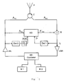
- FIG. 1 shows the structure of the arrangement according to the invention. It shows two mobile radio terminals M1, M2, which are connected via a plurality of second separating elements, which are combined to form an RF combiner, and a first separating element, which is a circulator Z, transmitting and receiving connected to the antenna A.
- the transmission stage PA in the transmission path and the amplifier stage LNA compensate for system losses through the coupling of the terminals with the antenna via the coupling network.
- the circulator reduces the overcoupling of the transmission signal from the transmission path in the reception path. Since it is not possible to sufficiently dimension the circulator attenuation of the transmission signal in the reception branch, a compensation circuit is provided which will be explained in more detail later in the description, in particular with reference to FIG.
- the arrangement presented here with the compensation circuit operates on the principle of adaptive interference cancellation. That is, a compensation signal is generated, which is ideally equal to the interfering signal at the input of the amplifier stage LNA to the sign. If one then adds this compensation signal and the disturbed received signal-that is, the input signal of the amplifier stage LNA-in the summing point S, then the interference signal caused by the transmission signal disappears.
- the compensation circuit is used with its associated two amount-forming detectors Det1, Det2.
- the interference signal is generated solely by the transmitter as the transmission signal A TX , which the noise signal at the LNA to a constant or slowly variable amplitude factor and a constant or slowly changing phase shift equalizes.
- This transmission signal A TX is provided to the compensation circuit KS in order to generate the compensation signal A ' RX therefrom by suitable adjustment of amplitude and phase, which is added to the disturbed reception signal in the disturbed reception path in the summation point S.
- the task of the compensation circuit is to adjust the amplitude and phase (or equivalently the I and Q component) of the compensation signal so that the interference component arising from the transmission signal in the received signal at the LNA input, ie at the summing point S, is reduced to zero or at least , This is done by minimizing the signal P. detected by the detector Det1.
- the two mixers MM_I and MM_Q on the right serve as actuators to set the I and Q component of the compensation signal.
- Input signals for the actuators are the signals alpha_I and alpha_Q, which are generated by the actual controller, the integrator Int_I, Int_Q.
- the arrangement is based on the orthogonality of the signals in the I and Q branch of two independent control loops R_I, R_Q; alpha_I affects only DI and alpha_Q affects only DQ. To describe the control behavior, it is therefore sufficient to consider only a portion of the complex signal path (in this case the 1-part). The other part is assumed to be correct in order to simplify the presentation. In other words, for the sake of simplification, only the (scalar) I channel is considered instead of the complex I / Q signal.
- a difficulty in the design of the scheme is that the sense of control is not known, as the following consideration shows: namely, if one carries the amplitude P of the sum signal L (Figure 1), as they from the detector to the compensation circuit KS, against the signal alpha_I (or alpha_Q) at the mixer input of MM_I (or MM_Q), for the open controlled system, results in a certain value for alpha_I (or the value pair alpha_I, alpha_Q) a minimum. For the scalar case (see above), these relationships are shown in FIG.
- the signal P and the 50 MHz signal originating from the local oscillator (LO) are multiplied together in the first mixer MD_I (or MD_Q) and thus a phase comparison and an amplitude weighting according to the amplitude of P are performed.
- Sign and amplitude of the output signal DI indicate control sense and control deviation.
- This signal can therefore serve as an input signal for the actual controller to the integrator Int_I, which in turn supplies the signals alpha_I or correspondingly alpha_Q.
- the controller is informed of an amplitude change of the transmission signal, as is the result of the ramping in the transmitter, via the input AGC and the gain of the integrator is thus adjusted.
- the first mixer MM_I (or MM_Q) now ensures that the transmission signal fed into it for the interference is amplitude-modulated with the sum of the integration result and the 50 MHz test signal.
- the resulting compensation signal is used to cancel out the noise signal at the LNA.
- the RF combiner in Figure 1 is explained in more detail with reference to FIG 4. He has the task, the two terminals - here mobile devices M1, M2 - to connect to the transmit and receive path while the transmission power of a device from the other device largely keep away, so that the reception is not disturbed on the latter.
- the circulators ensure the decoupling of the two terminals M1 and M2. So that transmitted RF power does not pass over the summation point (+) into the respective other terminal (M1 or M2), 2 transmission output stages PA are provided which prevent this by their reverse isolation.
- the described arrangement according to the invention shows a very good separation of the transmission path from the reception path and thus no or only a very slight overcoupling of the transmission power in the reception path. Thus, such disturbances in the received signal can be largely eliminated.
- the arrangement described is particularly suitable to be used in the context of a UMTS-TDD operation, which is made possible by their special separation performance.
Landscapes
- Engineering & Computer Science (AREA)
- Computer Networks & Wireless Communication (AREA)
- Signal Processing (AREA)
- Transceivers (AREA)
Claims (7)
- Arrangement pour faire fonctionner une pluralité de terminaux sur une antenne déportée commune comprenant un réseau de couplage, qui présente un premier élément de séparation associé à l'antenne, lequel sépare un chemin d'émission séparé destiné à transmettre un signal d'émission (ATX) et un chemin de réception séparé de celui-ci destiné à transmettre un signal de réception (ARX), caractérisé en ce que le chemin d'émission et le chemin de réception sont reliés ensemble par un circuit de compensation (KS) qui superpose au signal de réception (ARX) un signal de compensation (A'RX) dérivé du signal d'émission (ATX), le circuit de compensation (KS) étant configuré de telle sorte qu'un signal de compensation (A'RX) ayant la phase et l'amplitude correctes est formé avant un étage amplificateur en comparant le signal d'émission (ATX) et le signal de réception (ARX) ou un signal de réception superposé, et le circuit de compensation (KS) présente un étage de régulation qui minimise le signal d'amplitude (P) par déphasage et amplification ou atténuation du signal d'émission (ATX) acheminé et réduit ainsi l'influence du signal d'émission (ATX) sur le signal de réception (ARX), le circuit de compensation (KS) présentant une entrée pour le signal d'émission (ATX), une entrée pour un signal d'amplitude (P) déterminé à partir du signal de réception par un premier détecteur produisant une valeur (DET1), une entrée pour un signal d'amplification (AGC) déterminé à partir du signal d'émission par un deuxième détecteur produisant une valeur (DET2) et une sortie pour le signal de compensation (A'RX) ainsi que des circuits de régulation séparés (R_I, R_Q) pour former les parties I et Q du signal de compensation (A'RX) à partir du signal d'émission (ATX) et du signal de réception superposé, chaque circuit de régulation (R_I, R_Q) présentant un premier mélangeur (MM_I, MM_Q) auquel sont acheminés le signal d'émission (ATX) et un signal de régulation (alpha_I, alpha_Q), et chaque circuit de régulation (R_I, R_Q) présentant un deuxième mélangeur (MDI, MD_Q) auquel sont acheminés le signal d'amplitude (P) du premier détecteur (DET1) et un signal d'un oscillateur local (LO) et qui délivre un signal de sortie (D_I, D_Q) qui est acheminé en plus du signal d'amplification (AGC) à un intégrateur (Int_I, Int_Q) pour calculer le signal de régulation (alpha_I, alpha_Q).
- Arrangement pour faire fonctionner une pluralité de terminaux selon la revendication 1, caractérisé en ce que le réseau de couplage comprend un deuxième élément de séparation associé au terminal correspondant, au moins l'un des éléments de séparation étant configuré de telle sorte qu'il est possible d'y raccorder un chemin de communication individuel bidirectionnel menant d'un terminal au réseau de couplage, cet élément de séparation séparant ce chemin de communication bidirectionnel en des chemins d'émission et de réception acheminés séparément dans le réseau de couplage et le premier élément de séparation reliant les chemins d'émission et de réception communs avec l'antenne.
- Arrangement pour faire fonctionner une pluralité de terminaux selon la revendication 1 ou 2, caractérisé en ce que le chemin d'émission présente un étage d'émission (PA) et le chemin de réception un étage amplificateur (LNA) et qu'un prélèvement du signal d'émission (ATX) est prévu après l'étage d'émission (PA) en vue d'une retransmission au circuit de compensation (KS) ainsi qu'une superposition du signal de compensation (A'RX) généré dans le circuit de compensation avant l'étage amplificateur (LNA) dans un point d'addition (S).
- Arrangement pour faire fonctionner une pluralité de terminaux selon l'une des revendications précédentes, caractérisé en ce que le signal de sortie (D_I, D_Q), en plus du signal d'amplification (AGC), est acheminé à l'intégrateur (Int_I, Int_Q) pour ensuite être superposé avec le signal de l'oscillateur local (LO) dans un additionneur pour former le signal de régulation (alpha_I, alpha_Q).
- Arrangement pour faire fonctionner une pluralité de terminaux selon l'une des revendications précédentes, caractérisé en ce que les éléments de séparation représentent des circulateurs, des coupleurs directionnels, des éléments de commutation ou des éléments séparateurs de ligne en anneau.
- Arrangement pour faire fonctionner une pluralité de terminaux selon l'une des revendications précédentes, caractérisé en ce qu'il s'agit d'un arrangement destiné à fonctionner en mode TDD.
- Procédé pour faire fonctionner un arrangement comprenant une pluralité de terminaux sur une antenne déportée commune comprenant un réseau de couplage, qui présente un premier élément de séparation associé à l'antenne et un deuxième élément de séparation associé au terminal correspondant, au moins l'un des éléments de séparation étant réalisé de telle sorte qu'il est possible d'y raccorder un chemin de communication individuel bidirectionnel menant d'un terminal au réseau de couplage, cet élément de séparation séparant ce chemin de communication bidirectionnel en des chemins d'émission et de réception acheminés séparément dans le réseau de couplage et le premier élément de séparation reliant les chemins d'émission et de réception avec l'antenne, caractérisé en ce que le chemin d'émission et le chemin de réception sont reliés ensemble par un circuit de compensation (KS) qui, pour réduire le surcouplage du signal d'émission (ATX) sur le signal de réception (ARX), superpose au signal de réception (ARX) perturbé un signal de compensation (A'RX) dérivé du signal d'émission (ATX) et un signal de compensation (A'RX) ayant la phase et l'amplitude correctes étant formé dans le circuit de compensation avant un étage amplificateur en comparant le signal d'émission (ATX) et le signal de réception (ARX) ou un signal de réception superposé, et le circuit de compensation (KS) présente un étage de régulation qui minimise le signal d'amplitude (P) par déphasage et amplification ou atténuation du signal d'émission (ATX) acheminé et réduit ainsi l'influence du signal d'émission (ATX) sur le signal de réception (ARX), et le circuit de compensation (KS) présentant une entrée pour le signal d'émission (ATX), une entrée pour un signal d'amplitude (P) déterminé à partir du signal de réception par un premier détecteur produisant une valeur (DET1), une entrée pour un signal d'amplification (AGC) déterminé à partir du signal d'émission par un deuxième détecteur produisant une valeur (DET2) et une sortie pour le signal de compensation (A'RX) ainsi que des circuits de régulation séparés (R_I, R_Q) pour former les parties I et Q du signal de compensation (A'RX) à partir du signal d'émission (ATX) et du signal de réception superposé, chaque circuit de régulation (R_I, R_Q) présentant un premier mélangeur (MM_I, MM_Q) auquel sont acheminés le signal d'émission (ATX) et un signal de régulation (alpha_I, alpha_Q), et chaque circuit de régulation (R_I, R_Q) présentant un deuxième mélangeur (MDI, MD_Q) auquel sont acheminés le signal d'amplitude (P) du premier détecteur (DET1) et un signal d'un oscillateur local (LO) et qui délivre un signal de sortie (D_I, D_Q) qui est acheminé en plus du signal d'amplification (AGC) à un intégrateur (Int_I, Int_Q) pour calculer le signal de régulation (alpha_I, alpha_Q).
Applications Claiming Priority (3)
| Application Number | Priority Date | Filing Date | Title |
|---|---|---|---|
| DE2002155795 DE10255795A1 (de) | 2002-11-28 | 2002-11-28 | Anordnung zum Betrieb einer Mehrzahl von Endgeräten an einer gemeinsamen Antenne und Verfharen zum Betreiben einer solchen Anordnung |
| DE10255795 | 2002-11-28 | ||
| PCT/EP2003/012988 WO2004049506A1 (fr) | 2002-11-28 | 2003-11-20 | Systeme pour faire fonctionner une pluralite de terminaux sur une antenne commune et procede pour faire fonctionner ledit systeme |
Publications (2)
| Publication Number | Publication Date |
|---|---|
| EP1565962A1 EP1565962A1 (fr) | 2005-08-24 |
| EP1565962B1 true EP1565962B1 (fr) | 2006-06-28 |
Family
ID=32318804
Family Applications (1)
| Application Number | Title | Priority Date | Filing Date |
|---|---|---|---|
| EP03789061A Expired - Lifetime EP1565962B1 (fr) | 2002-11-28 | 2003-11-20 | Systeme pour faire fonctionner une pluralite de terminaux sur une antenne commune et procede pour faire fonctionner ledit systeme |
Country Status (4)
| Country | Link |
|---|---|
| EP (1) | EP1565962B1 (fr) |
| AU (1) | AU2003293707A1 (fr) |
| DE (2) | DE10255795A1 (fr) |
| WO (1) | WO2004049506A1 (fr) |
Family Cites Families (5)
| Publication number | Priority date | Publication date | Assignee | Title |
|---|---|---|---|---|
| GB923178A (en) * | 1960-12-22 | 1963-04-10 | Gen Electric Co Ltd | Improvements in or relating to radio apparatus for use in a continuous wave radio system |
| US5444864A (en) * | 1992-12-22 | 1995-08-22 | E-Systems, Inc. | Method and apparatus for cancelling in-band energy leakage from transmitter to receiver |
| DE19934502A1 (de) * | 1999-07-22 | 2001-01-25 | Siemens Ag | Funksende- und -empfangsgerät |
| DE10028189A1 (de) * | 2000-06-09 | 2001-12-20 | Daimler Chrysler Ag | Anordnung zum Betrieb mehrerer Endgeräte |
| WO2001095507A2 (fr) * | 2000-06-09 | 2001-12-13 | Daimlerchrysler Ag | Agencement pour faire fonctionner plusieurs terminaux |
-
2002
- 2002-11-28 DE DE2002155795 patent/DE10255795A1/de not_active Ceased
-
2003
- 2003-11-20 AU AU2003293707A patent/AU2003293707A1/en not_active Abandoned
- 2003-11-20 WO PCT/EP2003/012988 patent/WO2004049506A1/fr not_active Ceased
- 2003-11-20 DE DE50304087T patent/DE50304087D1/de not_active Expired - Lifetime
- 2003-11-20 EP EP03789061A patent/EP1565962B1/fr not_active Expired - Lifetime
Also Published As
| Publication number | Publication date |
|---|---|
| DE50304087D1 (de) | 2006-08-10 |
| DE10255795A1 (de) | 2004-06-17 |
| WO2004049506A1 (fr) | 2004-06-10 |
| AU2003293707A1 (en) | 2004-06-18 |
| EP1565962A1 (fr) | 2005-08-24 |
Similar Documents
| Publication | Publication Date | Title |
|---|---|---|
| DE60214368T2 (de) | Abstimmbarer phasenschieber und anwendungen dafür | |
| DE102009045546B4 (de) | Hochfrequenzschaltung mit verbesserter Antennenanpassung | |
| DE2453435C2 (de) | Schaltungsanordnung zur Kompensation von Polarisationsverzerrungen in einem Funksystem | |
| DE102006006291B4 (de) | Tranceiveranordnung und Verfahren zum Verarbeiten eines Signals | |
| DE69103036T2 (de) | Regenerierendes Zweiwege-RF-Verstärkersystem. | |
| DE69730939T2 (de) | Empfängerschaltung mit Raumdiversität | |
| DE60031976T2 (de) | Nachrichtengerät mit Kompensation von im Empfänger auftretenden Sender-Streusignalen | |
| EP2101278A2 (fr) | Circuit de compensation pour une unité de lecteur RFID et unité de lecteur RFID | |
| DE102004019587B3 (de) | Transceiver mit Störsignalunterdrückung und Verfahren zur Störsignalunterdrückung | |
| DE102008048986B4 (de) | Antennenverstärker und Empfangssystem | |
| DE69332320T2 (de) | Leistungsverstärkervorrichtung | |
| DE4229573A1 (de) | Funkempfaenger und -sender mit diversity | |
| DE102010064396A1 (de) | HF-Rückkopplungsempfängeranordnung, HF-Sendeanordnung und HF-Sende-Empfangsanordnung | |
| DE3600280A1 (de) | Kombinierte mehrfach-empfangsvorrichtung | |
| DE69736892T2 (de) | Nichtkohärentes Direktkonversionsempfänger mit Sechs-Tor-Schaltung | |
| EP1155501B1 (fr) | Emetteur a multiplexage en frequence et procede pour supprimer la diaphonie | |
| DE102004025576B4 (de) | Sende-und Empfangsanordnung mit einer Regelung zur Störsignalunterdrückung | |
| DE2334650B2 (de) | Trägerfrequenzmultiplexsystem | |
| EP0061582A2 (fr) | Procédé et circuit pour la compensation de la non-linéarité des éléments de transmission dans un système de transmission hertzienne dirigée | |
| EP1565962B1 (fr) | Systeme pour faire fonctionner une pluralite de terminaux sur une antenne commune et procede pour faire fonctionner ledit systeme | |
| DE69818075T2 (de) | Signalverarbeitungssystem | |
| DE2852120B2 (de) | Korrekturschaltung für Laufzeitröhren | |
| EP2011054B1 (fr) | Station de lecture/ecriture rfid de sensibilite elevee | |
| DE1002805B (de) | Als Funkrelaisstelle einsetzbares oder mit einer Drahtfernsprechleitung in Verbindung zu bringendes Funksprechgeraet | |
| EP0272510A2 (fr) | Dispositif de diversité d'espace |
Legal Events
| Date | Code | Title | Description |
|---|---|---|---|
| PUAI | Public reference made under article 153(3) epc to a published international application that has entered the european phase |
Free format text: ORIGINAL CODE: 0009012 |
|
| 17P | Request for examination filed |
Effective date: 20050418 |
|
| AK | Designated contracting states |
Kind code of ref document: A1 Designated state(s): AT BE BG CH CY CZ DE DK EE ES FI FR GB GR HU IE IT LI LU MC NL PT RO SE SI SK TR |
|
| AX | Request for extension of the european patent |
Extension state: AL LT LV MK |
|
| GRAP | Despatch of communication of intention to grant a patent |
Free format text: ORIGINAL CODE: EPIDOSNIGR1 |
|
| DAX | Request for extension of the european patent (deleted) | ||
| RBV | Designated contracting states (corrected) |
Designated state(s): DE |
|
| GRAS | Grant fee paid |
Free format text: ORIGINAL CODE: EPIDOSNIGR3 |
|
| GRAA | (expected) grant |
Free format text: ORIGINAL CODE: 0009210 |
|
| AK | Designated contracting states |
Kind code of ref document: B1 Designated state(s): DE |
|
| REF | Corresponds to: |
Ref document number: 50304087 Country of ref document: DE Date of ref document: 20060810 Kind code of ref document: P |
|
| RAP2 | Party data changed (patent owner data changed or rights of a patent transferred) |
Owner name: DAIMLERCHRYSLER AG |
|
| PLBE | No opposition filed within time limit |
Free format text: ORIGINAL CODE: 0009261 |
|
| STAA | Information on the status of an ep patent application or granted ep patent |
Free format text: STATUS: NO OPPOSITION FILED WITHIN TIME LIMIT |
|
| 26N | No opposition filed |
Effective date: 20070329 |
|
| PGFP | Annual fee paid to national office [announced via postgrant information from national office to epo] |
Ref country code: DE Payment date: 20150129 Year of fee payment: 12 |
|
| REG | Reference to a national code |
Ref country code: DE Ref legal event code: R119 Ref document number: 50304087 Country of ref document: DE |
|
| PG25 | Lapsed in a contracting state [announced via postgrant information from national office to epo] |
Ref country code: DE Free format text: LAPSE BECAUSE OF NON-PAYMENT OF DUE FEES Effective date: 20160601 |