EP1566880B1 - Procédé et dispositif pour charger le circuit intermediaire d'un convertisseur de frequence - Google Patents
Procédé et dispositif pour charger le circuit intermediaire d'un convertisseur de frequence Download PDFInfo
- Publication number
- EP1566880B1 EP1566880B1 EP05101106.2A EP05101106A EP1566880B1 EP 1566880 B1 EP1566880 B1 EP 1566880B1 EP 05101106 A EP05101106 A EP 05101106A EP 1566880 B1 EP1566880 B1 EP 1566880B1
- Authority
- EP
- European Patent Office
- Prior art keywords
- current
- charging
- semiconductor switch
- intermediate circuit
- frequency converter
- Prior art date
- Legal status (The legal status is an assumption and is not a legal conclusion. Google has not performed a legal analysis and makes no representation as to the accuracy of the status listed.)
- Expired - Lifetime
Links
- 238000000034 method Methods 0.000 title claims description 21
- 239000004065 semiconductor Substances 0.000 claims description 27
- 239000003990 capacitor Substances 0.000 claims description 18
- 230000007423 decrease Effects 0.000 claims description 4
- 238000012544 monitoring process Methods 0.000 claims 1
- 238000010304 firing Methods 0.000 description 2
- 230000001681 protective effect Effects 0.000 description 2
- 230000001360 synchronised effect Effects 0.000 description 2
- 238000005259 measurement Methods 0.000 description 1
Images

Classifications
-
- H—ELECTRICITY
- H02—GENERATION; CONVERSION OR DISTRIBUTION OF ELECTRIC POWER
- H02M—APPARATUS FOR CONVERSION BETWEEN AC AND AC, BETWEEN AC AND DC, OR BETWEEN DC AND DC, AND FOR USE WITH MAINS OR SIMILAR POWER SUPPLY SYSTEMS; CONVERSION OF DC OR AC INPUT POWER INTO SURGE OUTPUT POWER; CONTROL OR REGULATION THEREOF
- H02M1/00—Details of apparatus for conversion
- H02M1/32—Means for protecting converters other than automatic disconnection
-
- H—ELECTRICITY
- H02—GENERATION; CONVERSION OR DISTRIBUTION OF ELECTRIC POWER
- H02M—APPARATUS FOR CONVERSION BETWEEN AC AND AC, BETWEEN AC AND DC, OR BETWEEN DC AND DC, AND FOR USE WITH MAINS OR SIMILAR POWER SUPPLY SYSTEMS; CONVERSION OF DC OR AC INPUT POWER INTO SURGE OUTPUT POWER; CONTROL OR REGULATION THEREOF
- H02M1/00—Details of apparatus for conversion
- H02M1/16—Means for providing current step on switching, e.g. with saturable reactor
-
- H—ELECTRICITY
- H02—GENERATION; CONVERSION OR DISTRIBUTION OF ELECTRIC POWER
- H02M—APPARATUS FOR CONVERSION BETWEEN AC AND AC, BETWEEN AC AND DC, OR BETWEEN DC AND DC, AND FOR USE WITH MAINS OR SIMILAR POWER SUPPLY SYSTEMS; CONVERSION OF DC OR AC INPUT POWER INTO SURGE OUTPUT POWER; CONTROL OR REGULATION THEREOF
- H02M1/00—Details of apparatus for conversion
- H02M1/36—Means for starting or stopping converters
-
- H—ELECTRICITY
- H02—GENERATION; CONVERSION OR DISTRIBUTION OF ELECTRIC POWER
- H02M—APPARATUS FOR CONVERSION BETWEEN AC AND AC, BETWEEN AC AND DC, OR BETWEEN DC AND DC, AND FOR USE WITH MAINS OR SIMILAR POWER SUPPLY SYSTEMS; CONVERSION OF DC OR AC INPUT POWER INTO SURGE OUTPUT POWER; CONTROL OR REGULATION THEREOF
- H02M5/00—Conversion of AC power input into AC power output, e.g. for change of voltage, for change of frequency, for change of number of phases
- H02M5/40—Conversion of AC power input into AC power output, e.g. for change of voltage, for change of frequency, for change of number of phases with intermediate conversion into DC
- H02M5/42—Conversion of AC power input into AC power output, e.g. for change of voltage, for change of frequency, for change of number of phases with intermediate conversion into DC by static converters
- H02M5/44—Conversion of AC power input into AC power output, e.g. for change of voltage, for change of frequency, for change of number of phases with intermediate conversion into DC by static converters using discharge tubes or semiconductor devices to convert the intermediate DC into AC
- H02M5/453—Conversion of AC power input into AC power output, e.g. for change of voltage, for change of frequency, for change of number of phases with intermediate conversion into DC by static converters using discharge tubes or semiconductor devices to convert the intermediate DC into AC using devices of a triode or transistor type requiring continuous application of a control signal
- H02M5/458—Conversion of AC power input into AC power output, e.g. for change of voltage, for change of frequency, for change of number of phases with intermediate conversion into DC by static converters using discharge tubes or semiconductor devices to convert the intermediate DC into AC using devices of a triode or transistor type requiring continuous application of a control signal using semiconductor devices only
-
- H—ELECTRICITY
- H02—GENERATION; CONVERSION OR DISTRIBUTION OF ELECTRIC POWER
- H02M—APPARATUS FOR CONVERSION BETWEEN AC AND AC, BETWEEN AC AND DC, OR BETWEEN DC AND DC, AND FOR USE WITH MAINS OR SIMILAR POWER SUPPLY SYSTEMS; CONVERSION OF DC OR AC INPUT POWER INTO SURGE OUTPUT POWER; CONTROL OR REGULATION THEREOF
- H02M7/00—Conversion of AC power input into DC power output; Conversion of DC power input into AC power output
- H02M7/02—Conversion of AC power input into DC power output without possibility of reversal
- H02M7/04—Conversion of AC power input into DC power output without possibility of reversal by static converters
- H02M7/06—Conversion of AC power input into DC power output without possibility of reversal by static converters using discharge tubes without control electrode or semiconductor devices without control electrode
- H02M7/062—Avoiding or suppressing excessive transient voltages or currents
Definitions
- the present invention relates to a method and arrangement in a frequency converter as described in the preambles of independent claims 1 and 4.
- the invention relates to the charging of a capacitor of an intermediate circuit of frequency converters with voltage intermediate circuits.
- a frequency converter is a device used to generate an adjustable alternating voltage by using a constant-frequency voltage.
- the most typical application of frequency converters is controlling motors in such a manner that an adjustable voltage is generated from the alternating voltage of a supply network to control the motor.
- a frequency converter with a voltage intermediate circuit comprises a rectification unit, voltage intermediate circuit, and inverter unit.
- a task of the rectification unit is to provide direct voltage from the supplied alternating-current voltage to the voltage intermediate circuit, to which one or more capacitors are connected to store and equalize the direct voltage depending on the power of the device.
- the inverter unit connects the direct voltage of the voltage intermediate circuit to the load in such a manner that the direct voltage pulses generate the desired average alternating-current voltage or a corresponding adjustable property.
- the capacitor of the intermediate circuit When switching a frequency converter on, the capacitor of the intermediate circuit should be charged before the actual use of the frequency converter.
- the charging requires a separate charging arrangement that limits the magnitude of the charging current. If the charging current were not limited, the current would increase in magnitude so much that the protective devices in the supply would switch the supply voltage off.
- Known solutions for charging the capacitor of an intermediate circuit include various charging resistance arrangements, in which the charging current is reduced by a series resistor that is bypassed with a switch after the charging of the intermediate circuit.
- Another known way is to use a half-controlled bridge circuit, in which the magnitude of the charging current can be controlled by altering the firing angle of the controlled components of the bridge circuit, which requires that the charging arrangement be synchronized with the supply voltage.
- Document EP1363387A2 discloses a charging connection having a thyristor attached to a mains alternating current voltage.
- the thyristor has firing synchronized with a mains frequency for the duration of a charging process.
- the input diode bridge is by-passed using the thyristor.
- the invention is based on the fact that the voltage required for charging is generated with a separate rectifier bridge whose output current is directed to the frequency converter intermediate circuit to charge it.
- the charging current is controlled in such a manner that its value is kept within specific limit values. This way, the charging current is kept under control and does not cause any damage to the components of the frequency converter.
- the method and arrangement of the invention provide the advantage that they can be applied to frequency converters of all powers.
- the charging time varies depending on the magnitude of the capacitance of the frequency converter intermediate circuit.
- the method and arrangement of the invention provide significant space and cost savings.
- FIG. 1 is a general description of the arrangement of the invention.
- a rectifier 12 made up of the diodes of the frequency converter rectifies a voltage to an intermediate circuit capacitor 13.
- the rectifier 12 is supplied through chokes 10 and switching devices 11 from the network.
- means 20 connected to the frequency converter in accordance with the invention are used to charge the intermediate circuit.
- the means 20 for charging the intermediate circuit comprise a rectifier bridge 1, which is specifically a 6-pulse diode bridge, and a capacitor 2 connected to the output of the bridge.
- a task of the capacitor is to equalize the output voltage of the rectifier bridge.
- a direct voltage is formed at the output of the diode bridge 1 having a direct-current transformer 7 connected to its positive pole. This direct-current transformer generates a signal proportional to the charging current to a control circuit 4.
- the control circuit comprises a circuit for performing current measurement, control of the IGBT switch 5, and powering from the intermediate circuit 2.
- a semiconductor switch which in the embodiment of Figure 1 is an IGBT 5, is connected to the negative pole of the diode bridge output.
- a DC choke 8 is in series with the switch, and, to a point between these two, an anode of a zero diode 6 is connected, with its cathode connected to the positive pole of the diode bridge output.
- the second pole of the DC choke 8 is connected through a switch element 9 to the intermediate circuit of the frequency converter.
- the positive pole of the diode bridge is connected through a switch element 19 to the intermediate circuit of the frequency converter.
- the embodiment of Figure 1 shows how the charging arrangement supplies the capacitor 13 of the frequency converter intermediate circuit through the rectifier 12 of the frequency converter.
- the charging unit can be directly connected to the intermediate circuit of the frequency converter.
- a high current limit I hi and a low current limit I lo are defined in advance, and the charging current is maintained within the current range between the two limits during the charging of the capacitor of the intermediate circuit.
- the semiconductor switch 5 is made conductive to connect the output voltage of the diode bridge to the intermediate circuit of the frequency converter.
- the diode bridge 1 After the means for charging the intermediate circuit are switched on, i.e. after the switch elements 3 are made conductive, the diode bridge 1 generates in its output a direct-current voltage from the alternating-current voltage of its input, which is typically the voltage of the supply network.
- the control circuit 4 detects this voltage.
- Figure 1 shows how the control circuit is connected to both the positive and negative pole of the diode bridge output to detect this voltage and to generate its own operating voltage.
- the charging means 20 are connected to the intermediate circuit of the frequency converter through said switch 5, DC choke 8, closed switch 9, and the diode bridge of the frequency converter. Because the intermediate circuit of the frequency converter is dead, the current begins to run from the charging means to the intermediate circuit along the current path that has the direct-current transformer 7, a diode of the frequency converter diode bridge 12, the frequency converter intermediate circuit capacitor 13, a second diode of the frequency converter diode bridge 12, the DC choke 8, and the semiconductor switch 5. As the current runs to the intermediate circuit capacitor 13, the magnitude of this voltage increases.
- the direct-current transformer continuously monitors the magnitude of the charging current. Because the frequency converter intermediate circuit capacitor is, in practice, dead when the charging begins, the magnitude of the current increases rapidly, i.e. di/dt is high.
- the semiconductor switch is made non-conductive, i.e. the current path described above from the charging unit to the intermediate circuit is disconnected.
- the current path is disconnected, the current transfers, due to the DC choke 8, to the zero diode 6, and the current runs along a route that has the DC choke 8, zero diode 6, direct-current transformer 7 and the frequency converter intermediate circuit capacitor 13 through the diodes 12 of the rectifier. While this is the current path, the magnitude of the current begins to decrease.
- the control circuit 4 controls the switch 5 again to be conductive.
- Figure 2 shows by way of example the behaviour of the charging current I L depending on the ON/OFF state of the switch component.
- Figure 2 shows that when the switch component is conductive, the magnitude of the current increases.
- the switch component is made non-conductive, whereby the charging current I L d e-creases.
- the charging current reaches the low limit value I lo , the switch component is made conductive again, whereby the magnitude of the charging current increases.
- the charging current decreases and the hysteresis control no longer controls the switch component.
- the IGBT controls are stopped and information is transmitted to an upper control system that the charging is finished. This information is transmitted as a digital signal, for instance.
- the upper control system decides on closing the main switch device 11. When the switch elements 11 are closed, the intermediate circuit of the frequency converter receives its supply along the route used during operation.
- the switch elements 3, 9, 19 can also be opened, whereby the charging means are completely disconnected from both the supply network and the frequency converter.
- the embodiment of Figure 1 does not separately show that the same voltage, which typically is the supply network voltage, supplies the charging means 20 and the frequency converter.
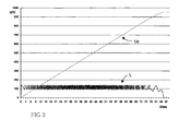
- Figure 3 shows the curve shapes of the charging current I L and the voltage of the intermediate circuit capacitor Uc produced by the method of the invention during charging.
- Figure 3 is based on charging with a 690-V supply voltage, in which the capacitance of the intermediate circuit being charged is 10 mF.
- Figure 3 shows how the charging current varies between 100 A and 140 A, which are the low and high limit values. If the capacitance of the intermediate circuit were higher, the charging would correspondingly take more time. The only variable in the charging is thus the time it takes. If the charging were made with conventional resistance charging, the charging current surge would be over 1000 A. This would considerably stress the charging contactor, and the wiring and protective fuses should be made very large.
- the charging time would increase in a conventional implementation, and the charging would necessarily not achieve a full charging level. If the intermediate circuit short-circuits during charging, for instance due to the failure of one of the power semiconductors, the method of the invention limits the short circuit current to the limit value set for the control circuit 4. In addition, the charging is automatically interrupted after the set maximum charging time.
Landscapes
- Engineering & Computer Science (AREA)
- Power Engineering (AREA)
- Rectifiers (AREA)
- Dc-Dc Converters (AREA)
- Charge And Discharge Circuits For Batteries Or The Like (AREA)
Claims (10)
- Procédé de charge d'un circuit intermédiaire dans un convertisseur de fréquence, le circuit intermédiaire du convertisseur de fréquence comprenant un ou plusieurs condensateurs et le convertisseur de fréquence comportant des moyens de charge du circuit intermédiaire, dans lequel les moyens de charge du circuit intermédiaire comprennent
un pont redresseur (1) qui comprend une entrée et une sortie, l'entrée étant connectée à une tension d'alimentation,
une bobine d'arrêt à courant continu (8),
un transformateur à courant continu (7),
une diode zéro (6), et
un commutateur à semi-conducteur (5) et un circuit de commande (4) agencé pour commander le commutateur ; le procédé comprenant les étapes de
définition à l'avance d'une limite de courant haute (Ihi) et d'une limite de courant basse (Ilo),
commande du commutateur à semi-conducteur (5) pour qu'il soit conducteur en vue de connecter la tension de sortie du pont redresseur (1) au circuit intermédiaire du convertisseur de fréquence,
surveillance en continu de la grandeur du courant de charge (IL) circulant des moyens de charge du circuit intermédiaire au circuit intermédiaire avec le transformateur à courant continu (7),
commande du commutateur à semi-conducteur (5) pour qu'il soit alternativement conducteur et non conducteur en fonction de la grandeur du courant de charge (IL) de telle manière que- lorsque le courant de charge diminue au niveau de la limite de courant basse (Ilo), le commutateur à semi-conducteur (5) est rendu conducteur, moyennant quoi la tension du pont redresseur (1) est connectée au circuit intermédiaire du convertisseur de fréquence et le courant de charge circule à travers le commutateur à semi-conducteur (5) et la bobine d'arrêt à courant continu (8), et- lorsque le courant de charge augmente au niveau de la limite de courant haute (Ihi), le commutateur à semi-conducteur (5) est rendu non conducteur, moyennant quoi la tension du pont redresseur (1) est déconnectée du circuit intermédiaire du convertisseur de fréquence et le courant de charge circule à travers la diode zéro (6) et la bobine d'arrêt à courant continu (8), etarrêt de la commande du commutateur à semi-conducteur (5) lorsque le courant de charge (IL) reste en dessous de la limite de courant haute (Ihi) alors que le commutateur à semi-conducteur est conducteur. - Procédé selon la revendication 1, dans lequel le procédé comprend les étapes de
définition du temps de charge maximal, et
arrêt de la commande du commutateur à semi-conducteur après que le temps de charge maximal est atteint. - Procédé selon la revendication 1 ou 2, dans lequel après que la commande du commutateur à semi-conducteur est arrêtée, une information est transmise à un système de commande supérieur selon laquelle la charge est finie.
- Procédé selon l'une quelconque des revendications 1 à 3, dans lequel le pont redresseur (1) est un pont de diode à 6 impulsions.
- Procédé selon l'une quelconque des revendications 1 à 3, dans lequel le commutateur à semi-conducteur (5) est un IGBT.
- Agencement de charge d'un circuit intermédiaire dans un convertisseur de fréquence, le convertisseur de fréquence comprenant un premier pont redresseur (12) connecté au circuit intermédiaire du convertisseur de fréquence comprenant un ou plusieurs condensateurs (13), et l'agencement comprenant un moyen (20) de charge du circuit intermédiaire, caractérisé en ce que le moyen (20) de charge du circuit intermédiaire comprend
un deuxième pont redresseur (1) qui comprend une entrée et une sortie, l'entrée étant agencée pour être connectée à la tension d'alimentation, et la sortie étant agencée pour générer une tension redressée,
un commutateur à semi-conducteur (5) et un circuit de commande (4) agencé pour commander le commutateur, le commutateur à semi-conducteur (5) étant connecté à la sortie du deuxième pont redresseur (1) dans le chemin de courant qui peut être formé entre le deuxième pont redresseur (1) et le circuit intermédiaire du convertisseur de fréquence,
une bobine d'arrêt à courant continu (8) et un transformateur à courant continu (7) qui sont connectés dans le chemin de courant qui peut être formé entre le deuxième pont redresseur et le circuit intermédiaire, et
une diode zéro (6) qui est connectée pour fournir un chemin de courant pour le courant de charge comprenant la bobine d'arrêt à courant continu (8) et le transformateur à courant continu (7) lorsque le chemin de courant pouvant être formé entre le deuxième pont redresseur (1) et le circuit intermédiaire est ouvert, moyennant quoi
le circuit de commande (4) du commutateur à semi-conducteur est agencé pour commander le commutateur à semi-conducteur pour qu'il soit alternativement conducteur et non conducteur en réponse à la grandeur de courant surveillée par le transformateur à courant continu (7) de telle manière que lorsque le courant diminue au niveau d'une limite de courant basse prédéfinie (Ilo), le commutateur à semi-conducteur (5) est rendu conducteur, et lorsque le courant augmente au niveau d'une limite de courant haute prédéfinie (Ihi), le commutateur à semi-conducteur (5) est rendu non conducteur, jusqu'à ce que le courant de charge reste en dessous de la limite de courant haute (Ihi) lorsque le commutateur à semi-conducteur est conducteur, auquel cas le circuit de commande (4) est agencé pour arrêter la charge en commandant le commutateur à semi-conducteur pour qu'il reste dans l'état non conducteur. - Agencement selon la revendication 6, dans lequel le circuit de commande (4) du commutateur à semi-conducteur est agencé pour arrêter la commande du commutateur à semi-conducteur lorsque le temps de charge maximal est atteint.
- Agencement selon la revendication 6 ou 7, dans lequel le pont redresseur (1) est un pont de diode à 6 impulsions.
- Agencement selon la revendication 6, 7 ou 8, dans lequel le commutateur à semi-conducteur (5) est un IGBT.
- Agencement selon l'une quelconque des revendications 6 à 9, dans lequel l'agencement comprend également des dispositifs de commutation (3, 9, 19) pour déconnecter les moyens de charge (20) du convertisseur de fréquence et de la tension d'alimentation.
Applications Claiming Priority (2)
| Application Number | Priority Date | Filing Date | Title |
|---|---|---|---|
| FI20045043 | 2004-02-18 | ||
| FI20045043A FI116758B (fi) | 2004-02-18 | 2004-02-18 | Menetelmä ja järjestely taajuusmuuttajan välipiirin lataamiseksi |
Publications (3)
| Publication Number | Publication Date |
|---|---|
| EP1566880A2 EP1566880A2 (fr) | 2005-08-24 |
| EP1566880A3 EP1566880A3 (fr) | 2012-12-26 |
| EP1566880B1 true EP1566880B1 (fr) | 2014-05-07 |
Family
ID=31725810
Family Applications (1)
| Application Number | Title | Priority Date | Filing Date |
|---|---|---|---|
| EP05101106.2A Expired - Lifetime EP1566880B1 (fr) | 2004-02-18 | 2005-02-15 | Procédé et dispositif pour charger le circuit intermediaire d'un convertisseur de frequence |
Country Status (3)
| Country | Link |
|---|---|
| US (1) | US6992908B2 (fr) |
| EP (1) | EP1566880B1 (fr) |
| FI (1) | FI116758B (fr) |
Families Citing this family (4)
| Publication number | Priority date | Publication date | Assignee | Title |
|---|---|---|---|---|
| NO20100985A1 (no) * | 2010-07-06 | 2011-11-21 | Rolls Royce Marine As Power Electric Systems Bergen | Styringsinnretning og fremgangsmåte for styring av en vekselstrømsmotor |
| EP2955834B1 (fr) * | 2014-06-12 | 2017-11-22 | ABB Technology Oy | Agencement de convertisseur |
| EP3001553A1 (fr) * | 2014-09-25 | 2016-03-30 | ABB Oy | Ensemble électrique |
| WO2017125769A1 (fr) * | 2016-01-18 | 2017-07-27 | University Of Split, Faculty Of Electrical Engineering, Mechanical Engineering And Naval Arichitecture | Système de précharge de liaison à courant continu dans des convertisseurs de fréquence frontaux actifs |
Family Cites Families (10)
| Publication number | Priority date | Publication date | Assignee | Title |
|---|---|---|---|---|
| GB1558596A (en) * | 1976-05-12 | 1980-01-09 | Tri Electronics Ab | Inverters |
| DE2728377A1 (de) * | 1977-06-23 | 1979-01-11 | Siemens Ag | Schaltungsanordnung zur umwandlung von elektrischer energie |
| JP2563338B2 (ja) * | 1987-06-02 | 1996-12-11 | 松下電器産業株式会社 | 低雑音コンバ−タ |
| SE515541C2 (sv) * | 1994-09-30 | 2001-08-27 | Emerson Energy Systems Ab | Anordning vid en likriktarbrygga |
| DE19639773A1 (de) * | 1996-09-27 | 1998-04-02 | Abb Patent Gmbh | Dreiphasiger Matrix-Stromrichter und Verfahren zum Betrieb |
| DE19642596A1 (de) * | 1996-10-15 | 1998-04-23 | Siemens Ag | Verfahren und Vorrichtung zur Kompensation von Blindstromanteilen mittels einer Kompensationseinrichtung mit einem Pulsstromrichter |
| DE10013391A1 (de) | 2000-03-17 | 2001-09-20 | Daimler Chrysler Ag | Vorladeeinrichtung für eine Stromrichterschaltung |
| DE10057783A1 (de) * | 2000-11-22 | 2002-06-06 | Siemens Ag | Verfahren zur Steuerung eines Matrixumrichters |
| FI111671B (fi) | 2001-10-25 | 2003-08-29 | Abb Industry Oy | Tasasuuntauspiiri |
| DE10221933A1 (de) * | 2002-05-17 | 2003-12-24 | Lenze Drive Systems Gmbh | Schaltungsanordnung für einen Gleichspannungszwischenkreis |
-
2004
- 2004-02-18 FI FI20045043A patent/FI116758B/fi not_active IP Right Cessation
-
2005
- 2005-02-15 EP EP05101106.2A patent/EP1566880B1/fr not_active Expired - Lifetime
- 2005-02-17 US US11/060,570 patent/US6992908B2/en not_active Expired - Fee Related
Also Published As
| Publication number | Publication date |
|---|---|
| EP1566880A3 (fr) | 2012-12-26 |
| EP1566880A2 (fr) | 2005-08-24 |
| FI20045043L (fi) | 2005-08-19 |
| US20050180185A1 (en) | 2005-08-18 |
| FI20045043A0 (fi) | 2004-02-18 |
| US6992908B2 (en) | 2006-01-31 |
| FI116758B (fi) | 2006-02-15 |
Similar Documents
| Publication | Publication Date | Title |
|---|---|---|
| US6801019B2 (en) | AC power generating system | |
| US9667157B1 (en) | System and method for operating a power converter | |
| EP2456060B1 (fr) | Circuit convertisseur de puissance | |
| US20080007190A1 (en) | Motor control apparatus and on-vehicle motor drive system | |
| US9768723B2 (en) | Motor drive using capacitor | |
| US10069444B2 (en) | Motor control apparatus having function of discharging energy remaining in DC link | |
| EP3098952A2 (fr) | Entraînement à faible capacité à immunité améliorée | |
| US5982649A (en) | Power supply circuit for a control circuit | |
| US9270192B2 (en) | Variable speed drive provided with a supercapacitor module | |
| US12126269B2 (en) | Inverter system | |
| EP2320545A1 (fr) | Convertisseur avec component pour limitation de la voltage | |
| US9419548B2 (en) | Method and control circuit for controlling a brushless electric motor | |
| EP1566880B1 (fr) | Procédé et dispositif pour charger le circuit intermediaire d'un convertisseur de frequence | |
| KR20110135126A (ko) | 캐스케이드 멀티레벨 고압인버터의 돌입전류 방지장치 | |
| KR101506010B1 (ko) | 무정전 전원장치의 직류단 전압 불평형 제어 장치 | |
| JP7760058B2 (ja) | 同期機用の励磁回路 | |
| US8891263B2 (en) | Inverter apparatus having power supply circuit | |
| JP2004208345A (ja) | 三相不平衡電圧抑制装置 | |
| US7456615B2 (en) | Charging arrangement for capacitor means | |
| EP4586480A1 (fr) | Commande d'amortissement combinée pour convertisseurs à thyristor redondants | |
| CN100386940C (zh) | 电力系统 | |
| JPH05252744A (ja) | 電源回路 |
Legal Events
| Date | Code | Title | Description |
|---|---|---|---|
| PUAI | Public reference made under article 153(3) epc to a published international application that has entered the european phase |
Free format text: ORIGINAL CODE: 0009012 |
|
| AK | Designated contracting states |
Kind code of ref document: A2 Designated state(s): AT BE BG CH CY CZ DE DK EE ES FI FR GB GR HU IE IS IT LI LT LU MC NL PL PT RO SE SI SK TR |
|
| AX | Request for extension of the european patent |
Extension state: AL BA HR LV MK YU |
|
| PUAL | Search report despatched |
Free format text: ORIGINAL CODE: 0009013 |
|
| AK | Designated contracting states |
Kind code of ref document: A3 Designated state(s): AT BE BG CH CY CZ DE DK EE ES FI FR GB GR HU IE IS IT LI LT LU MC NL PL PT RO SE SI SK TR |
|
| AX | Request for extension of the european patent |
Extension state: AL BA HR LV MK YU |
|
| RIC1 | Information provided on ipc code assigned before grant |
Ipc: H02M 7/06 20060101AFI20121120BHEP |
|
| 17P | Request for examination filed |
Effective date: 20130117 |
|
| 17Q | First examination report despatched |
Effective date: 20130301 |
|
| AKX | Designation fees paid |
Designated state(s): AT BE BG CH CY CZ DE DK EE ES FI FR GB GR HU IE IS IT LI LT LU MC NL PL PT RO SE SI SK TR |
|
| GRAP | Despatch of communication of intention to grant a patent |
Free format text: ORIGINAL CODE: EPIDOSNIGR1 |
|
| RIC1 | Information provided on ipc code assigned before grant |
Ipc: H02M 7/06 20060101ALI20130920BHEP Ipc: H02M 5/458 20060101AFI20130920BHEP Ipc: H02M 1/36 20070101ALI20130920BHEP |
|
| INTG | Intention to grant announced |
Effective date: 20131011 |
|
| GRAS | Grant fee paid |
Free format text: ORIGINAL CODE: EPIDOSNIGR3 |
|
| GRAA | (expected) grant |
Free format text: ORIGINAL CODE: 0009210 |
|
| AK | Designated contracting states |
Kind code of ref document: B1 Designated state(s): AT BE BG CH CY CZ DE DK EE ES FI FR GB GR HU IE IS IT LI LT LU MC NL PL PT RO SE SI SK TR |
|
| REG | Reference to a national code |
Ref country code: GB Ref legal event code: FG4D |
|
| REG | Reference to a national code |
Ref country code: AT Ref legal event code: REF Ref document number: 667343 Country of ref document: AT Kind code of ref document: T Effective date: 20140515 |
|
| REG | Reference to a national code |
Ref country code: IE Ref legal event code: FG4D |
|
| REG | Reference to a national code |
Ref country code: DE Ref legal event code: R096 Ref document number: 602005043515 Country of ref document: DE Effective date: 20140612 |
|
| REG | Reference to a national code |
Ref country code: AT Ref legal event code: MK05 Ref document number: 667343 Country of ref document: AT Kind code of ref document: T Effective date: 20140507 |
|
| REG | Reference to a national code |
Ref country code: NL Ref legal event code: VDEP Effective date: 20140507 |
|
| REG | Reference to a national code |
Ref country code: LT Ref legal event code: MG4D |
|
| PG25 | Lapsed in a contracting state [announced via postgrant information from national office to epo] |
Ref country code: FI Free format text: LAPSE BECAUSE OF FAILURE TO SUBMIT A TRANSLATION OF THE DESCRIPTION OR TO PAY THE FEE WITHIN THE PRESCRIBED TIME-LIMIT Effective date: 20140507 Ref country code: GR Free format text: LAPSE BECAUSE OF FAILURE TO SUBMIT A TRANSLATION OF THE DESCRIPTION OR TO PAY THE FEE WITHIN THE PRESCRIBED TIME-LIMIT Effective date: 20140808 Ref country code: IS Free format text: LAPSE BECAUSE OF FAILURE TO SUBMIT A TRANSLATION OF THE DESCRIPTION OR TO PAY THE FEE WITHIN THE PRESCRIBED TIME-LIMIT Effective date: 20140907 Ref country code: CY Free format text: LAPSE BECAUSE OF FAILURE TO SUBMIT A TRANSLATION OF THE DESCRIPTION OR TO PAY THE FEE WITHIN THE PRESCRIBED TIME-LIMIT Effective date: 20140507 Ref country code: LT Free format text: LAPSE BECAUSE OF FAILURE TO SUBMIT A TRANSLATION OF THE DESCRIPTION OR TO PAY THE FEE WITHIN THE PRESCRIBED TIME-LIMIT Effective date: 20140507 |
|
| PG25 | Lapsed in a contracting state [announced via postgrant information from national office to epo] |
Ref country code: PL Free format text: LAPSE BECAUSE OF FAILURE TO SUBMIT A TRANSLATION OF THE DESCRIPTION OR TO PAY THE FEE WITHIN THE PRESCRIBED TIME-LIMIT Effective date: 20140507 Ref country code: AT Free format text: LAPSE BECAUSE OF FAILURE TO SUBMIT A TRANSLATION OF THE DESCRIPTION OR TO PAY THE FEE WITHIN THE PRESCRIBED TIME-LIMIT Effective date: 20140507 Ref country code: SE Free format text: LAPSE BECAUSE OF FAILURE TO SUBMIT A TRANSLATION OF THE DESCRIPTION OR TO PAY THE FEE WITHIN THE PRESCRIBED TIME-LIMIT Effective date: 20140507 Ref country code: ES Free format text: LAPSE BECAUSE OF FAILURE TO SUBMIT A TRANSLATION OF THE DESCRIPTION OR TO PAY THE FEE WITHIN THE PRESCRIBED TIME-LIMIT Effective date: 20140507 |
|
| PG25 | Lapsed in a contracting state [announced via postgrant information from national office to epo] |
Ref country code: PT Free format text: LAPSE BECAUSE OF FAILURE TO SUBMIT A TRANSLATION OF THE DESCRIPTION OR TO PAY THE FEE WITHIN THE PRESCRIBED TIME-LIMIT Effective date: 20140908 |
|
| PG25 | Lapsed in a contracting state [announced via postgrant information from national office to epo] |
Ref country code: CZ Free format text: LAPSE BECAUSE OF FAILURE TO SUBMIT A TRANSLATION OF THE DESCRIPTION OR TO PAY THE FEE WITHIN THE PRESCRIBED TIME-LIMIT Effective date: 20140507 Ref country code: SK Free format text: LAPSE BECAUSE OF FAILURE TO SUBMIT A TRANSLATION OF THE DESCRIPTION OR TO PAY THE FEE WITHIN THE PRESCRIBED TIME-LIMIT Effective date: 20140507 Ref country code: RO Free format text: LAPSE BECAUSE OF FAILURE TO SUBMIT A TRANSLATION OF THE DESCRIPTION OR TO PAY THE FEE WITHIN THE PRESCRIBED TIME-LIMIT Effective date: 20140507 Ref country code: BE Free format text: LAPSE BECAUSE OF FAILURE TO SUBMIT A TRANSLATION OF THE DESCRIPTION OR TO PAY THE FEE WITHIN THE PRESCRIBED TIME-LIMIT Effective date: 20140507 Ref country code: EE Free format text: LAPSE BECAUSE OF FAILURE TO SUBMIT A TRANSLATION OF THE DESCRIPTION OR TO PAY THE FEE WITHIN THE PRESCRIBED TIME-LIMIT Effective date: 20140507 Ref country code: DK Free format text: LAPSE BECAUSE OF FAILURE TO SUBMIT A TRANSLATION OF THE DESCRIPTION OR TO PAY THE FEE WITHIN THE PRESCRIBED TIME-LIMIT Effective date: 20140507 |
|
| REG | Reference to a national code |
Ref country code: DE Ref legal event code: R097 Ref document number: 602005043515 Country of ref document: DE |
|
| REG | Reference to a national code |
Ref country code: FR Ref legal event code: PLFP Year of fee payment: 11 |
|
| PG25 | Lapsed in a contracting state [announced via postgrant information from national office to epo] |
Ref country code: NL Free format text: LAPSE BECAUSE OF FAILURE TO SUBMIT A TRANSLATION OF THE DESCRIPTION OR TO PAY THE FEE WITHIN THE PRESCRIBED TIME-LIMIT Effective date: 20140507 |
|
| PLBE | No opposition filed within time limit |
Free format text: ORIGINAL CODE: 0009261 |
|
| STAA | Information on the status of an ep patent application or granted ep patent |
Free format text: STATUS: NO OPPOSITION FILED WITHIN TIME LIMIT |
|
| 26N | No opposition filed |
Effective date: 20150210 |
|
| PGFP | Annual fee paid to national office [announced via postgrant information from national office to epo] |
Ref country code: DE Payment date: 20150219 Year of fee payment: 11 Ref country code: IT Payment date: 20150225 Year of fee payment: 11 |
|
| REG | Reference to a national code |
Ref country code: DE Ref legal event code: R097 Ref document number: 602005043515 Country of ref document: DE Effective date: 20150210 |
|
| PGFP | Annual fee paid to national office [announced via postgrant information from national office to epo] |
Ref country code: GB Payment date: 20150218 Year of fee payment: 11 Ref country code: FR Payment date: 20150219 Year of fee payment: 11 |
|
| PG25 | Lapsed in a contracting state [announced via postgrant information from national office to epo] |
Ref country code: SI Free format text: LAPSE BECAUSE OF FAILURE TO SUBMIT A TRANSLATION OF THE DESCRIPTION OR TO PAY THE FEE WITHIN THE PRESCRIBED TIME-LIMIT Effective date: 20140507 |
|
| PG25 | Lapsed in a contracting state [announced via postgrant information from national office to epo] |
Ref country code: LU Free format text: LAPSE BECAUSE OF FAILURE TO SUBMIT A TRANSLATION OF THE DESCRIPTION OR TO PAY THE FEE WITHIN THE PRESCRIBED TIME-LIMIT Effective date: 20150215 |
|
| REG | Reference to a national code |
Ref country code: CH Ref legal event code: PL |
|
| PG25 | Lapsed in a contracting state [announced via postgrant information from national office to epo] |
Ref country code: CH Free format text: LAPSE BECAUSE OF NON-PAYMENT OF DUE FEES Effective date: 20150228 Ref country code: LI Free format text: LAPSE BECAUSE OF NON-PAYMENT OF DUE FEES Effective date: 20150228 Ref country code: MC Free format text: LAPSE BECAUSE OF FAILURE TO SUBMIT A TRANSLATION OF THE DESCRIPTION OR TO PAY THE FEE WITHIN THE PRESCRIBED TIME-LIMIT Effective date: 20140507 |
|
| REG | Reference to a national code |
Ref country code: IE Ref legal event code: MM4A |
|
| PG25 | Lapsed in a contracting state [announced via postgrant information from national office to epo] |
Ref country code: IE Free format text: LAPSE BECAUSE OF NON-PAYMENT OF DUE FEES Effective date: 20150215 |
|
| REG | Reference to a national code |
Ref country code: DE Ref legal event code: R119 Ref document number: 602005043515 Country of ref document: DE |
|
| GBPC | Gb: european patent ceased through non-payment of renewal fee |
Effective date: 20160215 |
|
| REG | Reference to a national code |
Ref country code: FR Ref legal event code: ST Effective date: 20161028 |
|
| PG25 | Lapsed in a contracting state [announced via postgrant information from national office to epo] |
Ref country code: IT Free format text: LAPSE BECAUSE OF NON-PAYMENT OF DUE FEES Effective date: 20160215 |
|
| PG25 | Lapsed in a contracting state [announced via postgrant information from national office to epo] |
Ref country code: GB Free format text: LAPSE BECAUSE OF NON-PAYMENT OF DUE FEES Effective date: 20160215 Ref country code: DE Free format text: LAPSE BECAUSE OF NON-PAYMENT OF DUE FEES Effective date: 20160901 Ref country code: FR Free format text: LAPSE BECAUSE OF NON-PAYMENT OF DUE FEES Effective date: 20160229 |
|
| PG25 | Lapsed in a contracting state [announced via postgrant information from national office to epo] |
Ref country code: HU Free format text: LAPSE BECAUSE OF FAILURE TO SUBMIT A TRANSLATION OF THE DESCRIPTION OR TO PAY THE FEE WITHIN THE PRESCRIBED TIME-LIMIT; INVALID AB INITIO Effective date: 20050215 Ref country code: BG Free format text: LAPSE BECAUSE OF FAILURE TO SUBMIT A TRANSLATION OF THE DESCRIPTION OR TO PAY THE FEE WITHIN THE PRESCRIBED TIME-LIMIT Effective date: 20140507 |
|
| PG25 | Lapsed in a contracting state [announced via postgrant information from national office to epo] |
Ref country code: TR Free format text: LAPSE BECAUSE OF FAILURE TO SUBMIT A TRANSLATION OF THE DESCRIPTION OR TO PAY THE FEE WITHIN THE PRESCRIBED TIME-LIMIT Effective date: 20140507 |