EP2320545A1 - Convertisseur avec component pour limitation de la voltage - Google Patents
Convertisseur avec component pour limitation de la voltage Download PDFInfo
- Publication number
- EP2320545A1 EP2320545A1 EP10166956A EP10166956A EP2320545A1 EP 2320545 A1 EP2320545 A1 EP 2320545A1 EP 10166956 A EP10166956 A EP 10166956A EP 10166956 A EP10166956 A EP 10166956A EP 2320545 A1 EP2320545 A1 EP 2320545A1
- Authority
- EP
- European Patent Office
- Prior art keywords
- voltage
- terminal
- pole
- converter
- limiting component
- Prior art date
- Legal status (The legal status is an assumption and is not a legal conclusion. Google has not performed a legal analysis and makes no representation as to the accuracy of the status listed.)
- Granted
Links
Images


Classifications
-
- H—ELECTRICITY
- H02—GENERATION; CONVERSION OR DISTRIBUTION OF ELECTRIC POWER
- H02M—APPARATUS FOR CONVERSION BETWEEN AC AND AC, BETWEEN AC AND DC, OR BETWEEN DC AND DC, AND FOR USE WITH MAINS OR SIMILAR POWER SUPPLY SYSTEMS; CONVERSION OF DC OR AC INPUT POWER INTO SURGE OUTPUT POWER; CONTROL OR REGULATION THEREOF
- H02M1/00—Details of apparatus for conversion
- H02M1/32—Means for protecting converters other than automatic disconnection
-
- H—ELECTRICITY
- H02—GENERATION; CONVERSION OR DISTRIBUTION OF ELECTRIC POWER
- H02H—EMERGENCY PROTECTIVE CIRCUIT ARRANGEMENTS
- H02H9/00—Emergency protective circuit arrangements for limiting excess current or voltage without disconnection
- H02H9/04—Emergency protective circuit arrangements for limiting excess current or voltage without disconnection responsive to excess voltage
- H02H9/045—Emergency protective circuit arrangements for limiting excess current or voltage without disconnection responsive to excess voltage adapted to a particular application and not provided for elsewhere
- H02H9/046—Emergency protective circuit arrangements for limiting excess current or voltage without disconnection responsive to excess voltage adapted to a particular application and not provided for elsewhere responsive to excess voltage appearing at terminals of integrated circuits
-
- H—ELECTRICITY
- H02—GENERATION; CONVERSION OR DISTRIBUTION OF ELECTRIC POWER
- H02M—APPARATUS FOR CONVERSION BETWEEN AC AND AC, BETWEEN AC AND DC, OR BETWEEN DC AND DC, AND FOR USE WITH MAINS OR SIMILAR POWER SUPPLY SYSTEMS; CONVERSION OF DC OR AC INPUT POWER INTO SURGE OUTPUT POWER; CONTROL OR REGULATION THEREOF
- H02M1/00—Details of apparatus for conversion
- H02M1/0083—Converters characterised by their input or output configuration
- H02M1/0085—Partially controlled bridges
Definitions
- the invention relates to a method for protecting semiconductor components in a converter against overvoltages.
- the invention also relates to a converter with overvoltage protection.
- Many power electronic converters such as frequency converters, for example, include a converter bridge adapted to transfer electrical energy between the AC mains and the DC terminal of the converter.
- Said DC terminal can be represented by the positive and negative rails in the intermediate DC link of a frequency converter, for instance.
- the converter bridge often includes controlled semiconductor components such as thyristors or transistors, for example.
- the converter bridge may also be a half-controlled bridge in which only one branch, connected with the positive or negative pole of said DC terminal, includes controlled semiconductor components, while the opposite branch includes diodes. Diodes and other semiconductor components have to be protected against potential overvoltage transients occurring in the AC mains.
- Thyristors for instance, have a turn-on delay of 2 ⁇ s, approximately, during which time the forward voltage in the thyristor may rise detrimentally high even if a firing pulse were continuously delivered to the thyristor. If the circuit connected with the thyristor has a small inductance and the forward voltage of the thyristor is too high at the turn-on moment, the rate of change of current (di/dt, A/s) may become so high that the thyristor becomes damaged. For diodes, on the other hand, a typical damaging mechanism is a breakdown caused by a reverse voltage too high.
- AC chokes are placed between the AC mains and the converter bridge to filter out overvoltage transients occurring in the AC mains and to restrict the rates of change of current in the semiconductor components in the converter bridge.
- a drawback of said AC chokes is that they increase the load-dependent voltage drop of the DC voltage in the DC terminal.
- said AC chokes increase the commutation angle and thus decrease the DC voltage and affect the power factor at the DC terminal.
- a converter according to the invention comprises:
- the invention is also directed to a novel method for protecting semiconductor components in a converter bridge against overvoltages, the converter bridge being adapted to transfer electrical energy between the AC terminal and DC terminal of the converter.
- overvoltage transients occurring in said AC terminal are conducted into said DC terminal via electrical paths provided between each of the phases of said AC terminal and said DC terminal, each path comprising a unidirectionally conductive semiconductor component and a voltage-limiting component in which the ratio of voltage to current is greater than a predetermined value in response to a situation where the voltage across the voltage-limiting component is smaller than a predetermined threshold voltage, and in which the ratio of voltage change to current change is smaller than said predetermined value in response to a situation where the voltage across the voltage-limiting component is greater than said threshold voltage.
- the voltage-limiting component may be e.g. a varistor or a transient voltage suppressor (TVS).
- the unidirectionally conductive semiconductor component may be e.g. a diode or a transistor the control terminal of which is connected to another terminal; e.g. a bipolar transistor the base of which is connected to the emitter or the collector depending on the type of the transistor. Because of the overvoltage protection thus achieved, AC chokes can be omitted from the AC terminal or at least they can be designed smaller, reducing the load-dependent voltage drop of the DC terminal.
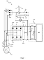
- Fig. 1 is a schematic illustration of a converter 100 according to an embodiment of the invention.
- the converter comprises a converter bridge 101 adapted to transfer electrical energy from the AC terminal 102 to the DC terminal 103 of the converter. Through the AC terminal 102 the converter is connected to the AC mains 114, and through the DC terminal 103 the converter bridge 101 is connected to the block 115 which loads the converter bridge.
- the converter may be e.g. a frequency converter, in which case the block 113 comprises an inverter bridge.
- the converter bridge 101 is a half-controlled rectifier bridge with thyristors 109 in the upper branch and diodes 110 in the lower branch. By means of the thyristors 109 the converter bridge can be turned off when necessary, e.g.
- the thyristors 109 may also be used for regulating the DC voltage output by the converter bridge 101. It should be noted that the converter bridge in the converter may be different than that depicted in Fig. 1 .
- the converter bridge may be e.g. a mains inverter bridge in which each of the diodes 110 and each of the thyristors 109 is replaced by a transistor such as an insulated gate bipolar transistor (IGBT) and a diode in reverse parallel connection.
- the converter comprises electrical paths bypassing the converter bridge 101 for conducting overvoltage transients occurring in the AC terminal 102 around the converter bridge 101 to the DC terminal 103 and further to a capacitor 111.
- the electrical paths have diodes 104a, 104b, and 104c and a voltage-limiting component 105 which may be e.g. a varistor or a transient voltage suppressor (TVS).
- the ratio of voltage to current (u/i, ⁇ ) in the voltage-limiting component 105 is greater than a predetermined value R when the voltage U v across the voltage-limiting component is smaller than a predetermined threshold voltage U th , and the ratio of voltage change to current change (du/di, ⁇ ) is considerably smaller than said predetermined value R when the voltage U v across the voltage-limiting component is greater than said threshold voltage U th .
- the current through the voltage-limiting component is smaller than U v /R, and when U v > U th , the voltage U v across the voltage-limiting component will substantially not increase even if the current through the voltage-limiting component increases, because the ratio of voltage change to current change du/di is small.
- the ratio of voltage change to current change (du/di) may be e.g. smaller than R/10 when U v > U th .
- the diodes 104a, 104b, and 104c are connected, all in the same direction, between the phases 102a, 102b, and 102c of the AC terminal 102 and a first pole of the voltage-limiting component 105.
- a second pole of the voltage-limiting component 105 is connected to a first pole 103a of the DC terminal 103 which in the converter depicted in Fig. 1 is the positive pole of the DC terminal.
- the maximum forward voltage across each of the thyristors 109 substantially equals the threshold voltage U th of the voltage-limiting component 105 because the diodes 104a, 104b, and 104c, which are adapted to conduct electric current towards the positive pole of the DC terminal 103, will choose the highest one of the potentials in the phases 102a, 102b, and 102c of the AC terminal 102 for the voltage-limiting component 105.
- Limiting the forward voltage of the thyristor also limits the rate of change of current (di/dt) following the firing of the thyristor and thus protects the thyristor from being damaged.
- a threshold voltage U th of 60 V for instance, can be chosen for the voltage-limiting component 105.
- the second pole of the voltage-limiting component 105 is connected to the first pole 103a of the DC terminal via a switch 106 by means of which the voltage-limiting component can be disconnected from said first pole e.g. for the duration of the charging of the capacitors 111 and 112.
- a resistor 107 in parallel with the series connection comprised of the voltage-limiting component 105 and switch 106.
- the diodes 104a, 104b, and 104c and the resistor 107 can be used together with the diodes 110 to charge the capacitors 111 and 112 when the switch 106 is in a nonconducting state.
- a second voltage-limiting component 108 for which the ratio of voltage to current (u/i) is greater than a predetermined value R when the voltage U v2 across the voltage-limiting component is smaller than a predetermined threshold voltage U th2 , and the ratio of voltage change to current change (du/di) is considerably smaller than said predetermined value R when the voltage U v2 across the voltage-limiting component is greater than said threshold voltage U th2 .
- the voltage-limiting component 108 may be e.g. a varistor or a transient voltage suppressor (TVS).
- the maximum reverse voltage across each of the diodes 110 substantially equals the threshold voltage U th2 because the diodes 104a, 104b, and 104c will choose the highest one of the potentials in the phases 102a, 102b, and 102c of the AC terminal 102 for the voltage-limiting component 108.
- the threshold voltage U th2 of the voltage-limiting component 108 can be the voltage which the diodes 110 can withstand minus a safety margin.
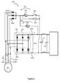
- Fig. 2 is a schematic illustration of a converter 200 according to an embodiment of the invention.
- the converter comprises a converter bridge 201 adapted to transfer electrical energy from the AC terminal 202 to the DC terminal 203 of the converter.
- the converter bridge 201 is a half-controlled rectifier bridge with thyristors 209 in the lower branch and diodes 210 in the upper branch unlike in the case depicted in Fig. 1 where there were diodes in the lower branch and thyristors in the upper branch.
- the converter comprises electrical paths bypassing the converter bridge 201 for conducting overvoltage transients occurring in the AC terminal 202 around the converter bridge 201 to the DC terminal 203 and further to a capacitor 211.
- a voltage-limiting component 205 for which the ratio of voltage to current (u/i) is greater than a predetermined value R when the voltage U v across the voltage-limiting component is smaller than a predetermined threshold voltage U th , and the ratio of voltage change to current change (du/di) is considerably smaller than said predetermined value R when the voltage U v across the voltage-limiting component is greater than said threshold voltage U th .
- the voltage-limiting component 205 may be e.g. a varistor or a transient voltage suppressor (TVS).
- TVS transient voltage suppressor
- One pole of the voltage-limiting component 205 is connected to a first pole 203a of the DC terminal 203 which in the case depicted in Fig. 2 is the negative pole of the DC terminal.
- the maximum forward voltage across each of the thyristors 209 substantially equals said threshold voltage U th because the diodes 204a, 204b, and 204c, which are adapted to conduct electric current towards the AC terminal 203, will choose the smallest one of the potentials in the phases 202a, 202b, and 202c of the AC terminal 202 for the first pole of the voltage-limiting component 205.
- a second voltage-limiting component 208 for which the ratio of voltage to current (u/i) is greater than a predetermined value R when the voltage U v2 across the voltage-limiting component is smaller than a predetermined threshold voltage U th2 , and the ratio of voltage change to current change (du/di) is considerably smaller than said predetermined value R when the voltage U v2 across the voltage-limiting component is greater than said threshold voltage U th2 .
- the maximum reverse voltage across each of the diodes 210 substantially equals the threshold voltage U th2 because the diodes 204a, 204b, and 204c will choose the smallest one of the potentials in the phases 202a, 202b, and 202c of the AC terminal 202 for the voltage-limiting component 208.
- the threshold voltage U th2 of the voltage-limiting component 208 can be set at the voltage which the diodes 210 can withstand minus a safety margin.
- the voltage-limiting component 205 is connected to a first pole 203a of the DC terminal via a switch 206 by means of which the voltage-limiting component can be disconnected from said first pole e.g. for the duration of the charging of the capacitors 211 and 212.
- a resistor 207 in parallel with the series connection comprised of the voltage-limiting component 205 and switch 206.
- the diodes 204a, 204b, and 204c and the resistor 207 can be used together with the diodes 210 to charge the capacitors 211 and 212 when the switch 206 is in a nonconducting state.
- Fig. 3 is a schematic illustration of a converter 300 according to an embodiment of the invention.
- the converter comprises a converter bridge 301 adapted to transfer electrical energy from the AC terminal 302 to the DC terminal 303 of the converter.
- the converter bridge 301 is a half-controlled rectifier bridge with thyristors 309 in the upper branch and diodes 310 in the lower branch.
- the converter comprises electrical paths bypassing the converter bridge 301 for conducting overvoltage transients occurring in the AC terminal 302 around the converter bridge 301 to the DC terminal 303 and further to a capacitor 311.
- phase 302a of the AC terminal 302 and a first pole 303a of the DC terminal 303 there is a series connection comprised of a voltage-limiting component 305a and a diode 304a
- a series connection comprised of a voltage-limiting component 305b and a diode 304b
- the first pole 303a of the DC terminal 303 is the positive pole of the DC terminal.
- the maximum forward voltage across each of the thyristors 309 substantially equals the threshold voltage of the voltage-limiting components 305a and 305b.
- Fig. 4 is a flow chart illustrating a method according to an embodiment of the invention for protecting semiconductor components in a converter bridge against overvoltages.
- the method comprises a step, block 401, for conducting overvoltage transients occurring in said AC terminal into said DC terminal via electrical paths between each of the phases of the AC terminal and a first pole of the DC terminal, each electrical path comprising a unidirectionally conductive semiconductor component and a voltage-limiting component.
- the ratio of voltage to current (u/i) in the voltage-limiting component is greater than a predetermined value R when the voltage across the voltage-limiting component is smaller than a predetermined threshold voltage, and the ratio of voltage change to current change (du/di) is considerably smaller than said value R when the voltage is greater than said threshold voltage.
- the voltage-limiting component is a varistor, and in a method according to another embodiment of the invention the voltage-limiting component is a transient voltage suppressor (TVS).
- TVS transient voltage suppressor
- the voltage-limiting component in each of said electrical paths is common to said electrical paths.
- a first pole of the voltage-limiting component is connected to a first pole of the DC terminal, and a second pole of the voltage-limiting component is connected with the unidirectionally conductive semiconductor components of the electrical paths, said semiconductor components being connected mutually in the same direction.
- the reverse voltage in the semiconductor components of said converter bridge is limited by means of a second voltage-limiting component located between a first pole of said voltage-limiting component and a second pole of said DC terminal, which second voltage-limiting component may be a varistor or a transient voltage suppressor (TVS), for example.
- second voltage-limiting component may be a varistor or a transient voltage suppressor (TVS), for example.
- said first pole of the DC terminal is the positive pole of the DC terminal and each unidirectionally conductive semiconductor component is arranged to conduct electric current towards the positive pole of the DC terminal.
- said first pole of the DC terminal is the negative pole of the DC terminal and each unidirectionally conductive semiconductor component is arranged to conduct electric current towards the AC terminal.
- the unidirectionally conductive semiconductor component is a diode.
Landscapes
- Engineering & Computer Science (AREA)
- Power Engineering (AREA)
- Microelectronics & Electronic Packaging (AREA)
- Rectifiers (AREA)
Applications Claiming Priority (1)
| Application Number | Priority Date | Filing Date | Title |
|---|---|---|---|
| FI20095852A FI122449B (fi) | 2009-08-18 | 2009-08-18 | Suuntaajalaite |
Publications (2)
| Publication Number | Publication Date |
|---|---|
| EP2320545A1 true EP2320545A1 (fr) | 2011-05-11 |
| EP2320545B1 EP2320545B1 (fr) | 2018-09-26 |
Family
ID=41050680
Family Applications (1)
| Application Number | Title | Priority Date | Filing Date |
|---|---|---|---|
| EP10166956.2A Active EP2320545B1 (fr) | 2009-08-18 | 2010-06-23 | Convertisseur avec component pour limitation de la voltage |
Country Status (3)
| Country | Link |
|---|---|
| US (1) | US8670253B2 (fr) |
| EP (1) | EP2320545B1 (fr) |
| FI (1) | FI122449B (fr) |
Cited By (1)
| Publication number | Priority date | Publication date | Assignee | Title |
|---|---|---|---|---|
| CN107528480A (zh) * | 2016-06-20 | 2017-12-29 | 光宝电子(广州)有限公司 | 具有雷击保护能力的电路 |
Families Citing this family (7)
| Publication number | Priority date | Publication date | Assignee | Title |
|---|---|---|---|---|
| US20120146402A1 (en) * | 2010-12-09 | 2012-06-14 | Siemens Industry, Inc. | Control system for regulating bus voltage for an electric shovel |
| US20140146586A1 (en) * | 2011-04-15 | 2014-05-29 | Siemens Aktiengesellschaft | Multilevel converter and method of starting up a multilevel converter |
| ITFI20130236A1 (it) | 2013-10-10 | 2015-04-11 | Power One Italy Spa | Dispositivo di protezione da correnti transitorie per sistemi di conversione di energia elettrica connessi alla rete. |
| DE102014006365B4 (de) * | 2014-04-30 | 2022-08-11 | Sew-Eurodrive Gmbh & Co Kg | Vorrichtung zum Betreiben eines Gleichrichters, insbesondere einer halbgesteuerten Gleichrichterbrücke, und Verfahren zum Betreiben eines Gleichrichters |
| JP6539896B2 (ja) * | 2015-02-20 | 2019-07-10 | 三菱造船株式会社 | 船舶推進システム、船舶及び船舶推進方法 |
| CN110311366B (zh) * | 2018-03-27 | 2022-03-01 | 台达电子工业股份有限公司 | 电源转换电路的雷击保护装置 |
| FR3087614B1 (fr) * | 2018-10-19 | 2020-10-09 | Sagemcom Energy & Telecom Sas | Carte electrique comprenant un pont de redressement |
Citations (1)
| Publication number | Priority date | Publication date | Assignee | Title |
|---|---|---|---|---|
| DD257533B5 (de) * | 1987-02-02 | 1994-05-11 | Elpro Ag | Verfahren zum Betrieb einer untersynchronen Stromrichterkaskade |
Family Cites Families (12)
| Publication number | Priority date | Publication date | Assignee | Title |
|---|---|---|---|---|
| HU178854B (en) * | 1980-04-09 | 1982-07-28 | Kohaszati Gyarepitoe Vallalat | Rectified,reversing drive supplied from alternating current mains brakeable in both rotation sense advantageously for motor control gear of arc furnace |
| JPH088778B2 (ja) * | 1987-04-22 | 1996-01-29 | 株式会社日立製作所 | 電流形インバ−タ装置 |
| DE3835869A1 (de) * | 1988-10-21 | 1990-04-26 | Asea Brown Boveri | Anordnung zum starten eines wechselrichters |
| WO1991018441A1 (fr) * | 1989-04-19 | 1991-11-28 | Square D Company | Alimentation electrique |
| DE4034723C2 (de) | 1990-10-29 | 1995-10-05 | Elpro Ag | Verfahren zum Schutz von netzgeführten Wechselrichtern |
| DE9216662U1 (de) | 1992-12-07 | 1993-01-28 | Siemens AG, 80333 München | Vorladeschaltung mit kombiniertem Überspannungsschutz für einen netzgeführten Stromrichter mit ausgangsseitigem Kondensator |
| BE1010412A3 (nl) | 1996-07-09 | 1998-07-07 | Philips Electronics Nv | Schakelinrichting. |
| DE19710371C1 (de) | 1997-03-13 | 1998-09-03 | Semikron Elektronik Gmbh | Schaltungsanordnung zum Aufladen von Zwischenkreisen |
| US6226166B1 (en) * | 1997-11-28 | 2001-05-01 | Erico Lighting Technologies Pty Ltd | Transient overvoltage and lightning protection of power connected equipment |
| FI111671B (fi) * | 2001-10-25 | 2003-08-29 | Abb Industry Oy | Tasasuuntauspiiri |
| FI121492B (fi) * | 2005-04-22 | 2010-11-30 | Vacon Oyj | Taajuusmuuttajan ylijännitesuojaus |
| TW200826444A (en) * | 2006-07-27 | 2008-06-16 | Koninkl Philips Electronics Nv | Switch mode power supply for in-line voltage applications |
-
2009
- 2009-08-18 FI FI20095852A patent/FI122449B/fi not_active IP Right Cessation
-
2010
- 2010-06-23 EP EP10166956.2A patent/EP2320545B1/fr active Active
- 2010-07-16 US US12/837,682 patent/US8670253B2/en active Active
Patent Citations (1)
| Publication number | Priority date | Publication date | Assignee | Title |
|---|---|---|---|---|
| DD257533B5 (de) * | 1987-02-02 | 1994-05-11 | Elpro Ag | Verfahren zum Betrieb einer untersynchronen Stromrichterkaskade |
Non-Patent Citations (1)
| Title |
|---|
| HABERBERGER M ET AL: "Novel protection strategy for current interruptions in IGBT current source inverters", POWER ELECTRONICS SPECIALISTS CONFERENCE, 2004. PESC 04. 2004 IEEE 35TH ANNUAL, AACHEN, GERMANY 20-25 JUNE 2004, PISCATAWAY, NJ, USA,IEEE, US, 20 June 2004 (2004-06-20), pages 558 - 564VOL.1, XP010738049, ISBN: 978-0-7803-8399-9, DOI: 10.1109/PESC.2004.1355808 * |
Cited By (1)
| Publication number | Priority date | Publication date | Assignee | Title |
|---|---|---|---|---|
| CN107528480A (zh) * | 2016-06-20 | 2017-12-29 | 光宝电子(广州)有限公司 | 具有雷击保护能力的电路 |
Also Published As
| Publication number | Publication date |
|---|---|
| FI20095852A0 (fi) | 2009-08-18 |
| FI20095852L (fi) | 2011-02-19 |
| FI122449B (fi) | 2012-01-31 |
| US20110044080A1 (en) | 2011-02-24 |
| US8670253B2 (en) | 2014-03-11 |
| EP2320545B1 (fr) | 2018-09-26 |
Similar Documents
| Publication | Publication Date | Title |
|---|---|---|
| EP2320545A1 (fr) | Convertisseur avec component pour limitation de la voltage | |
| US11139808B2 (en) | Semiconductor device and power conversion system | |
| CN106253649B (zh) | 具有短路装置的电力变换器子模块和具有其的电力变换器 | |
| KR101994143B1 (ko) | 컨버터 장치 및 그 단락 보호 방법 | |
| KR101832868B1 (ko) | 직류를 스위칭하기 위한 디바이스 | |
| US20100321847A1 (en) | Semiconductor power conversion apparatus | |
| US9979286B2 (en) | Power converting device | |
| US11108320B2 (en) | Method and voltage multiplier for converting an input voltage, and disconnector | |
| JP2009506736A (ja) | 分散配置されたエネルギー蓄積器を有する電力変換回路 | |
| EP3068023A1 (fr) | Limiteur d'appel pour convertisseurs de puissance ca/ca d'un entraînement par moteur | |
| CN211930497U (zh) | 变换器模块和电压中间电路变换器 | |
| US10523011B2 (en) | Voltage compensation apparatus for photovoltaic system and photovoltaic system | |
| US20140285126A1 (en) | Method and control circuit for controlling a brushless electric motor | |
| US12407342B2 (en) | Drive circuit to drive power semiconductor element, power semiconductor module, and power conversion device | |
| US12407270B2 (en) | Voltage converter | |
| CN107210298A (zh) | 用于保护由电网运行的单元免受过压的电路装置 | |
| Alwash et al. | Short-circuit protection of power converters with SiC current limiters | |
| CN211320924U (zh) | 硬件快速过压抑制电路 | |
| JP2018157702A (ja) | 電圧補償装置 | |
| EP1566880B1 (fr) | Procédé et dispositif pour charger le circuit intermediaire d'un convertisseur de frequence | |
| EP4333288A1 (fr) | Démarreur de moteur à semi-conducteurs | |
| CN214205325U (zh) | 一种过压保护电路及电子设备 | |
| EP3229356A1 (fr) | Alimentation électrique avec circuit de protection par court-circuit à base mosfet | |
| KR20180040376A (ko) | 전력 변환 장치 및 이를 포함하는 공기 조화기 | |
| JP3891015B2 (ja) | 半導体装置 |
Legal Events
| Date | Code | Title | Description |
|---|---|---|---|
| PUAI | Public reference made under article 153(3) epc to a published international application that has entered the european phase |
Free format text: ORIGINAL CODE: 0009012 |
|
| AK | Designated contracting states |
Kind code of ref document: A1 Designated state(s): AL AT BE BG CH CY CZ DE DK EE ES FI FR GB GR HR HU IE IS IT LI LT LU LV MC MK MT NL NO PL PT RO SE SI SK SM TR |
|
| AX | Request for extension of the european patent |
Extension state: BA ME RS |
|
| 17P | Request for examination filed |
Effective date: 20110518 |
|
| RAP1 | Party data changed (applicant data changed or rights of an application transferred) |
Owner name: VACON OY |
|
| GRAP | Despatch of communication of intention to grant a patent |
Free format text: ORIGINAL CODE: EPIDOSNIGR1 |
|
| STAA | Information on the status of an ep patent application or granted ep patent |
Free format text: STATUS: GRANT OF PATENT IS INTENDED |
|
| INTG | Intention to grant announced |
Effective date: 20180426 |
|
| GRAS | Grant fee paid |
Free format text: ORIGINAL CODE: EPIDOSNIGR3 |
|
| GRAA | (expected) grant |
Free format text: ORIGINAL CODE: 0009210 |
|
| STAA | Information on the status of an ep patent application or granted ep patent |
Free format text: STATUS: THE PATENT HAS BEEN GRANTED |
|
| AK | Designated contracting states |
Kind code of ref document: B1 Designated state(s): AL AT BE BG CH CY CZ DE DK EE ES FI FR GB GR HR HU IE IS IT LI LT LU LV MC MK MT NL NO PL PT RO SE SI SK SM TR |
|
| REG | Reference to a national code |
Ref country code: GB Ref legal event code: FG4D |
|
| REG | Reference to a national code |
Ref country code: CH Ref legal event code: EP |
|
| REG | Reference to a national code |
Ref country code: AT Ref legal event code: REF Ref document number: 1047191 Country of ref document: AT Kind code of ref document: T Effective date: 20181015 |
|
| REG | Reference to a national code |
Ref country code: IE Ref legal event code: FG4D |
|
| REG | Reference to a national code |
Ref country code: DE Ref legal event code: R096 Ref document number: 602010053821 Country of ref document: DE |
|
| REG | Reference to a national code |
Ref country code: NL Ref legal event code: MP Effective date: 20180926 |
|
| PG25 | Lapsed in a contracting state [announced via postgrant information from national office to epo] |
Ref country code: SE Free format text: LAPSE BECAUSE OF FAILURE TO SUBMIT A TRANSLATION OF THE DESCRIPTION OR TO PAY THE FEE WITHIN THE PRESCRIBED TIME-LIMIT Effective date: 20180926 Ref country code: LT Free format text: LAPSE BECAUSE OF FAILURE TO SUBMIT A TRANSLATION OF THE DESCRIPTION OR TO PAY THE FEE WITHIN THE PRESCRIBED TIME-LIMIT Effective date: 20180926 Ref country code: FI Free format text: LAPSE BECAUSE OF FAILURE TO SUBMIT A TRANSLATION OF THE DESCRIPTION OR TO PAY THE FEE WITHIN THE PRESCRIBED TIME-LIMIT Effective date: 20180926 Ref country code: GR Free format text: LAPSE BECAUSE OF FAILURE TO SUBMIT A TRANSLATION OF THE DESCRIPTION OR TO PAY THE FEE WITHIN THE PRESCRIBED TIME-LIMIT Effective date: 20181227 Ref country code: BG Free format text: LAPSE BECAUSE OF FAILURE TO SUBMIT A TRANSLATION OF THE DESCRIPTION OR TO PAY THE FEE WITHIN THE PRESCRIBED TIME-LIMIT Effective date: 20181226 Ref country code: NO Free format text: LAPSE BECAUSE OF FAILURE TO SUBMIT A TRANSLATION OF THE DESCRIPTION OR TO PAY THE FEE WITHIN THE PRESCRIBED TIME-LIMIT Effective date: 20181226 |
|
| REG | Reference to a national code |
Ref country code: LT Ref legal event code: MG4D |
|
| PG25 | Lapsed in a contracting state [announced via postgrant information from national office to epo] |
Ref country code: AL Free format text: LAPSE BECAUSE OF FAILURE TO SUBMIT A TRANSLATION OF THE DESCRIPTION OR TO PAY THE FEE WITHIN THE PRESCRIBED TIME-LIMIT Effective date: 20180926 Ref country code: HR Free format text: LAPSE BECAUSE OF FAILURE TO SUBMIT A TRANSLATION OF THE DESCRIPTION OR TO PAY THE FEE WITHIN THE PRESCRIBED TIME-LIMIT Effective date: 20180926 Ref country code: LV Free format text: LAPSE BECAUSE OF FAILURE TO SUBMIT A TRANSLATION OF THE DESCRIPTION OR TO PAY THE FEE WITHIN THE PRESCRIBED TIME-LIMIT Effective date: 20180926 |
|
| REG | Reference to a national code |
Ref country code: AT Ref legal event code: MK05 Ref document number: 1047191 Country of ref document: AT Kind code of ref document: T Effective date: 20180926 |
|
| PG25 | Lapsed in a contracting state [announced via postgrant information from national office to epo] |
Ref country code: PL Free format text: LAPSE BECAUSE OF FAILURE TO SUBMIT A TRANSLATION OF THE DESCRIPTION OR TO PAY THE FEE WITHIN THE PRESCRIBED TIME-LIMIT Effective date: 20180926 Ref country code: AT Free format text: LAPSE BECAUSE OF FAILURE TO SUBMIT A TRANSLATION OF THE DESCRIPTION OR TO PAY THE FEE WITHIN THE PRESCRIBED TIME-LIMIT Effective date: 20180926 Ref country code: EE Free format text: LAPSE BECAUSE OF FAILURE TO SUBMIT A TRANSLATION OF THE DESCRIPTION OR TO PAY THE FEE WITHIN THE PRESCRIBED TIME-LIMIT Effective date: 20180926 Ref country code: NL Free format text: LAPSE BECAUSE OF FAILURE TO SUBMIT A TRANSLATION OF THE DESCRIPTION OR TO PAY THE FEE WITHIN THE PRESCRIBED TIME-LIMIT Effective date: 20180926 Ref country code: IS Free format text: LAPSE BECAUSE OF FAILURE TO SUBMIT A TRANSLATION OF THE DESCRIPTION OR TO PAY THE FEE WITHIN THE PRESCRIBED TIME-LIMIT Effective date: 20190126 Ref country code: ES Free format text: LAPSE BECAUSE OF FAILURE TO SUBMIT A TRANSLATION OF THE DESCRIPTION OR TO PAY THE FEE WITHIN THE PRESCRIBED TIME-LIMIT Effective date: 20180926 Ref country code: RO Free format text: LAPSE BECAUSE OF FAILURE TO SUBMIT A TRANSLATION OF THE DESCRIPTION OR TO PAY THE FEE WITHIN THE PRESCRIBED TIME-LIMIT Effective date: 20180926 Ref country code: IT Free format text: LAPSE BECAUSE OF FAILURE TO SUBMIT A TRANSLATION OF THE DESCRIPTION OR TO PAY THE FEE WITHIN THE PRESCRIBED TIME-LIMIT Effective date: 20180926 Ref country code: CZ Free format text: LAPSE BECAUSE OF FAILURE TO SUBMIT A TRANSLATION OF THE DESCRIPTION OR TO PAY THE FEE WITHIN THE PRESCRIBED TIME-LIMIT Effective date: 20180926 |
|
| PG25 | Lapsed in a contracting state [announced via postgrant information from national office to epo] |
Ref country code: PT Free format text: LAPSE BECAUSE OF FAILURE TO SUBMIT A TRANSLATION OF THE DESCRIPTION OR TO PAY THE FEE WITHIN THE PRESCRIBED TIME-LIMIT Effective date: 20190126 Ref country code: SM Free format text: LAPSE BECAUSE OF FAILURE TO SUBMIT A TRANSLATION OF THE DESCRIPTION OR TO PAY THE FEE WITHIN THE PRESCRIBED TIME-LIMIT Effective date: 20180926 Ref country code: SK Free format text: LAPSE BECAUSE OF FAILURE TO SUBMIT A TRANSLATION OF THE DESCRIPTION OR TO PAY THE FEE WITHIN THE PRESCRIBED TIME-LIMIT Effective date: 20180926 |
|
| REG | Reference to a national code |
Ref country code: DE Ref legal event code: R097 Ref document number: 602010053821 Country of ref document: DE |
|
| PG25 | Lapsed in a contracting state [announced via postgrant information from national office to epo] |
Ref country code: DK Free format text: LAPSE BECAUSE OF FAILURE TO SUBMIT A TRANSLATION OF THE DESCRIPTION OR TO PAY THE FEE WITHIN THE PRESCRIBED TIME-LIMIT Effective date: 20180926 |
|
| PLBE | No opposition filed within time limit |
Free format text: ORIGINAL CODE: 0009261 |
|
| STAA | Information on the status of an ep patent application or granted ep patent |
Free format text: STATUS: NO OPPOSITION FILED WITHIN TIME LIMIT |
|
| 26N | No opposition filed |
Effective date: 20190627 |
|
| PG25 | Lapsed in a contracting state [announced via postgrant information from national office to epo] |
Ref country code: SI Free format text: LAPSE BECAUSE OF FAILURE TO SUBMIT A TRANSLATION OF THE DESCRIPTION OR TO PAY THE FEE WITHIN THE PRESCRIBED TIME-LIMIT Effective date: 20180926 |
|
| PG25 | Lapsed in a contracting state [announced via postgrant information from national office to epo] |
Ref country code: MC Free format text: LAPSE BECAUSE OF FAILURE TO SUBMIT A TRANSLATION OF THE DESCRIPTION OR TO PAY THE FEE WITHIN THE PRESCRIBED TIME-LIMIT Effective date: 20180926 |
|
| REG | Reference to a national code |
Ref country code: CH Ref legal event code: PL |
|
| GBPC | Gb: european patent ceased through non-payment of renewal fee |
Effective date: 20190623 |
|
| REG | Reference to a national code |
Ref country code: BE Ref legal event code: MM Effective date: 20190630 |
|
| PG25 | Lapsed in a contracting state [announced via postgrant information from national office to epo] |
Ref country code: TR Free format text: LAPSE BECAUSE OF FAILURE TO SUBMIT A TRANSLATION OF THE DESCRIPTION OR TO PAY THE FEE WITHIN THE PRESCRIBED TIME-LIMIT Effective date: 20180926 |
|
| PG25 | Lapsed in a contracting state [announced via postgrant information from national office to epo] |
Ref country code: IE Free format text: LAPSE BECAUSE OF NON-PAYMENT OF DUE FEES Effective date: 20190623 Ref country code: GB Free format text: LAPSE BECAUSE OF NON-PAYMENT OF DUE FEES Effective date: 20190623 |
|
| PG25 | Lapsed in a contracting state [announced via postgrant information from national office to epo] |
Ref country code: CH Free format text: LAPSE BECAUSE OF NON-PAYMENT OF DUE FEES Effective date: 20190630 Ref country code: BE Free format text: LAPSE BECAUSE OF NON-PAYMENT OF DUE FEES Effective date: 20190630 Ref country code: LI Free format text: LAPSE BECAUSE OF NON-PAYMENT OF DUE FEES Effective date: 20190630 Ref country code: LU Free format text: LAPSE BECAUSE OF NON-PAYMENT OF DUE FEES Effective date: 20190623 |
|
| PG25 | Lapsed in a contracting state [announced via postgrant information from national office to epo] |
Ref country code: FR Free format text: LAPSE BECAUSE OF NON-PAYMENT OF DUE FEES Effective date: 20190630 |
|
| PG25 | Lapsed in a contracting state [announced via postgrant information from national office to epo] |
Ref country code: CY Free format text: LAPSE BECAUSE OF FAILURE TO SUBMIT A TRANSLATION OF THE DESCRIPTION OR TO PAY THE FEE WITHIN THE PRESCRIBED TIME-LIMIT Effective date: 20180926 |
|
| PG25 | Lapsed in a contracting state [announced via postgrant information from national office to epo] |
Ref country code: HU Free format text: LAPSE BECAUSE OF FAILURE TO SUBMIT A TRANSLATION OF THE DESCRIPTION OR TO PAY THE FEE WITHIN THE PRESCRIBED TIME-LIMIT; INVALID AB INITIO Effective date: 20100623 Ref country code: MT Free format text: LAPSE BECAUSE OF FAILURE TO SUBMIT A TRANSLATION OF THE DESCRIPTION OR TO PAY THE FEE WITHIN THE PRESCRIBED TIME-LIMIT Effective date: 20180926 |
|
| PG25 | Lapsed in a contracting state [announced via postgrant information from national office to epo] |
Ref country code: MK Free format text: LAPSE BECAUSE OF FAILURE TO SUBMIT A TRANSLATION OF THE DESCRIPTION OR TO PAY THE FEE WITHIN THE PRESCRIBED TIME-LIMIT Effective date: 20180926 |
|
| P01 | Opt-out of the competence of the unified patent court (upc) registered |
Effective date: 20230621 |
|
| PGFP | Annual fee paid to national office [announced via postgrant information from national office to epo] |
Ref country code: DE Payment date: 20250507 Year of fee payment: 16 |
|
| REG | Reference to a national code |
Ref country code: DE Ref legal event code: R081 Ref document number: 602010053821 Country of ref document: DE Owner name: DANFOSS DRIVES OY, FI Free format text: FORMER OWNER: VACON OY, VAASA, FI |