EP1568038B1 - Verfahren und vorrichtung zum erkennen des beginns einer thermischen relaxation in magnetischen datenspeichern - Google Patents
Verfahren und vorrichtung zum erkennen des beginns einer thermischen relaxation in magnetischen datenspeichern Download PDFInfo
- Publication number
- EP1568038B1 EP1568038B1 EP03758590A EP03758590A EP1568038B1 EP 1568038 B1 EP1568038 B1 EP 1568038B1 EP 03758590 A EP03758590 A EP 03758590A EP 03758590 A EP03758590 A EP 03758590A EP 1568038 B1 EP1568038 B1 EP 1568038B1
- Authority
- EP
- European Patent Office
- Prior art keywords
- magnetic
- elements
- storage elements
- data storage
- memory device
- Prior art date
- Legal status (The legal status is an assumption and is not a legal conclusion. Google has not performed a legal analysis and makes no representation as to the accuracy of the status listed.)
- Expired - Lifetime
Links
- 230000005291 magnetic effect Effects 0.000 title claims abstract description 180
- 238000013500 data storage Methods 0.000 title claims abstract description 45
- 238000000034 method Methods 0.000 title claims description 26
- 238000003860 storage Methods 0.000 claims abstract description 57
- 230000005415 magnetization Effects 0.000 claims abstract description 42
- 230000015654 memory Effects 0.000 claims description 75
- 230000008569 process Effects 0.000 claims description 10
- 239000000696 magnetic material Substances 0.000 claims description 8
- 238000012545 processing Methods 0.000 claims description 7
- 239000010409 thin film Substances 0.000 claims description 5
- 238000001514 detection method Methods 0.000 abstract description 4
- 230000011664 signaling Effects 0.000 abstract description 3
- 239000010410 layer Substances 0.000 description 28
- 230000007704 transition Effects 0.000 description 15
- 239000000523 sample Substances 0.000 description 14
- 238000012360 testing method Methods 0.000 description 10
- 230000004888 barrier function Effects 0.000 description 9
- 239000010408 film Substances 0.000 description 9
- 238000009826 distribution Methods 0.000 description 8
- 239000013598 vector Substances 0.000 description 8
- 238000012544 monitoring process Methods 0.000 description 6
- 239000011229 interlayer Substances 0.000 description 5
- 239000011159 matrix material Substances 0.000 description 5
- 230000036961 partial effect Effects 0.000 description 5
- 230000000694 effects Effects 0.000 description 4
- 230000005293 ferrimagnetic effect Effects 0.000 description 4
- 230000005294 ferromagnetic effect Effects 0.000 description 4
- 230000006870 function Effects 0.000 description 4
- 230000005381 magnetic domain Effects 0.000 description 4
- 239000002245 particle Substances 0.000 description 4
- 230000002829 reductive effect Effects 0.000 description 4
- 230000005641 tunneling Effects 0.000 description 4
- 238000003491 array Methods 0.000 description 3
- 230000006399 behavior Effects 0.000 description 3
- 239000004020 conductor Substances 0.000 description 3
- 230000001419 dependent effect Effects 0.000 description 3
- 230000000670 limiting effect Effects 0.000 description 3
- 239000000463 material Substances 0.000 description 3
- 238000004088 simulation Methods 0.000 description 3
- 241001581440 Astroides Species 0.000 description 2
- 229910001030 Iron–nickel alloy Inorganic materials 0.000 description 2
- 230000008901 benefit Effects 0.000 description 2
- 230000008859 change Effects 0.000 description 2
- 230000014759 maintenance of location Effects 0.000 description 2
- 230000010287 polarization Effects 0.000 description 2
- 230000009467 reduction Effects 0.000 description 2
- 239000007787 solid Substances 0.000 description 2
- 230000006641 stabilisation Effects 0.000 description 2
- 239000000758 substrate Substances 0.000 description 2
- 229910017107 AlOx Inorganic materials 0.000 description 1
- 229910019222 CoCrPt Inorganic materials 0.000 description 1
- 238000013019 agitation Methods 0.000 description 1
- 238000004458 analytical method Methods 0.000 description 1
- 230000005290 antiferromagnetic effect Effects 0.000 description 1
- 238000013459 approach Methods 0.000 description 1
- 230000002301 combined effect Effects 0.000 description 1
- 239000002131 composite material Substances 0.000 description 1
- 238000010276 construction Methods 0.000 description 1
- 230000005611 electricity Effects 0.000 description 1
- 230000001747 exhibiting effect Effects 0.000 description 1
- 230000004907 flux Effects 0.000 description 1
- 230000003993 interaction Effects 0.000 description 1
- 238000001459 lithography Methods 0.000 description 1
- 239000006249 magnetic particle Substances 0.000 description 1
- 238000004519 manufacturing process Methods 0.000 description 1
- 238000001465 metallisation Methods 0.000 description 1
- 238000012986 modification Methods 0.000 description 1
- 230000004048 modification Effects 0.000 description 1
- 230000008520 organization Effects 0.000 description 1
- 230000000704 physical effect Effects 0.000 description 1
- 230000002441 reversible effect Effects 0.000 description 1
- 238000013112 stability test Methods 0.000 description 1
- 238000011105 stabilization Methods 0.000 description 1
- 230000003068 static effect Effects 0.000 description 1
Images


Classifications
-
- G—PHYSICS
- G11—INFORMATION STORAGE
- G11C—STATIC STORES
- G11C11/00—Digital stores characterised by the use of particular electric or magnetic storage elements; Storage elements therefor
- G11C11/02—Digital stores characterised by the use of particular electric or magnetic storage elements; Storage elements therefor using magnetic elements
- G11C11/16—Digital stores characterised by the use of particular electric or magnetic storage elements; Storage elements therefor using magnetic elements using elements in which the storage effect is based on magnetic spin effect
-
- G—PHYSICS
- G11—INFORMATION STORAGE
- G11C—STATIC STORES
- G11C11/00—Digital stores characterised by the use of particular electric or magnetic storage elements; Storage elements therefor
- G11C11/02—Digital stores characterised by the use of particular electric or magnetic storage elements; Storage elements therefor using magnetic elements
- G11C11/14—Digital stores characterised by the use of particular electric or magnetic storage elements; Storage elements therefor using magnetic elements using thin-film elements
- G11C11/15—Digital stores characterised by the use of particular electric or magnetic storage elements; Storage elements therefor using magnetic elements using thin-film elements using multiple magnetic layers
-
- G—PHYSICS
- G11—INFORMATION STORAGE
- G11C—STATIC STORES
- G11C29/00—Checking stores for correct operation ; Subsequent repair; Testing stores during standby or offline operation
- G11C29/04—Detection or location of defective memory elements, e.g. cell constructio details, timing of test signals
- G11C29/50—Marginal testing, e.g. race, voltage or current testing
-
- H—ELECTRICITY
- H10—SEMICONDUCTOR DEVICES; ELECTRIC SOLID-STATE DEVICES NOT OTHERWISE PROVIDED FOR
- H10B—ELECTRONIC MEMORY DEVICES
- H10B61/00—Magnetic memory devices, e.g. magnetoresistive RAM [MRAM] devices
- H10B61/20—Magnetic memory devices, e.g. magnetoresistive RAM [MRAM] devices comprising components having three or more electrodes, e.g. transistors
- H10B61/22—Magnetic memory devices, e.g. magnetoresistive RAM [MRAM] devices comprising components having three or more electrodes, e.g. transistors of the field-effect transistor [FET] type
-
- H—ELECTRICITY
- H10—SEMICONDUCTOR DEVICES; ELECTRIC SOLID-STATE DEVICES NOT OTHERWISE PROVIDED FOR
- H10N—ELECTRIC SOLID-STATE DEVICES NOT OTHERWISE PROVIDED FOR
- H10N50/00—Galvanomagnetic devices
- H10N50/10—Magnetoresistive devices
-
- G—PHYSICS
- G11—INFORMATION STORAGE
- G11C—STATIC STORES
- G11C29/00—Checking stores for correct operation ; Subsequent repair; Testing stores during standby or offline operation
- G11C29/04—Detection or location of defective memory elements, e.g. cell constructio details, timing of test signals
- G11C29/50—Marginal testing, e.g. race, voltage or current testing
- G11C2029/5002—Characteristic
Definitions
- the present invention relates to magnetic memory or data storage devices, in particular to such magnetic memory devices with small size magnetic elements, i.e. in the order of 100 nm and smaller.
- the present invention relates to a method and a device to detect the likely onset of thermal relaxation in magnetic data storage devices.
- magnetic materials in data storage devices is well established, either as the data storage medium (hard disk, magneto-optic disk, floppy disk, tape, MRAM data storage layer/element, etc.), read-back sensor (MR, GMR, TMR hard disk heads, MRAM sense elements, etc.) or write elements (hard disk, magneto-optic disk, floppy disk and tape write head flux guides, etc.).
- bit density i.e. the amount of data that can be stored in one unit square (e.g. centimetre 2 ) of surface area of recording medium
- bit density i.e. the amount of data that can be stored in one unit square (e.g. centimetre 2 ) of surface area of recording medium
- a dramatic reduction of the bit (and thus magnetic domain) size has been realized in order to increase data capacity.
- the signal to noise ratio of a recording medium is strongly related to the number of grains. As bit sizes are scaled down to increase areal densities, the average grain volume in each bit of the medium is also being reduced in order to maintain enough grains per bit to ensure an acceptable signal to noise ratio.
- the magnetization of a magnet decays with time, due to random thermal fluctuations (k B T), sometimes in conjunction with the effect of an external field, overcoming the magnetic (anisotropy) energy (K u V) of the material.
- K B T random thermal fluctuations
- K u V magnetic energy
- the particle becomes super-paramagnetic, i.e. the magnetization of the particle switches randomly over short time scales.
- the super-paramagnetic limit the magnetic particles are so small that they cannot maintain a stable magnetization for any practically useful amount of time, which results in data loss. This physical limit depends upon temperature and the physical and structural properties of the magnetic material.
- Bit or memory element (and thus magnetic domain) sizes cannot be reduced indefinitely as a physical limit, the above-mentioned super-paramagnetic limit, exists for the smallest magnetically stable volume.
- the grain magnetization being susceptible to thermal agitation leads to a reduced signal to noise ratio (in hard disks) and eventual loss of data (in both hard disks and MRAM) as bits or memory elements effectively "self-erase”.
- Using materials with large intrinsic anisotropy constants, or large shape anisotropies e.g. elongated ellipsoids), can delay the onset of this super-paramagnetic limit.
- anti-ferromagnetically coupled (AFC) media have recently been described by Fujitsu and IBM, E. Abarra et al., "Longitudinal recording media with thermal stabilization layers", J. Appl. Phys. Lett. 77, (2000) p.2581 ; E. Fullerton et al., " Antiferromagnetically coupled magnetic media layers for thermally stable high-density recording", J. Appl. Phys. Lett. 77, (2000) p.3806 .
- Such a medium called a synthetic antiferromagnetic medium (AFC)
- AFC consists of two conventional crystalline data storage layers of different thickness and possessing in-plane magnetic anisotropy, that are exchange coupled through a thin Ru interlayer. This approach stabilizes the medium against thermal fluctuations by effectively increasing the effective magnetic volume of each bit.
- a third strategy is to switch to using patterned media consisting of small physically separated magnetic islands, usually possessing perpendicular magnetic anisotropy. If of suitable dimensions, such islands will possess a high shape anisotropy, or be too small to support magnetic domains, and hence exhibit an enhanced thermal stability. This is described in M. Albrecht et al., "Thermal stability and recording properties of sub-100 nm patterned CoCrPt perpendicular media", J. Appl. Phys. Lett. 91 (2002), p.6849 .
- Small magnetic islands are also required for the memory elements of MRAM devices. Again the thermal stability of such elements may be enhanced by the use of magnetic materials possessing high intrinsic magnetic anisotropy, or by engineering the shape of the magnetic islands such that they possess a large shape anisotropy.
- D1 describes an MRAM array wherein storage MRAM cells are provided and reference MRAM cells are provided.
- the reference cells are provided to supply a reference current for a sensing amplifier to determine a logic state of the MRAM cells to be read. It is mentioned that deviations and fluctuations are the same for the reference cells as for the cells to be read.
- Both MRAM data storage elements and magnetic recording media are subject to the super-paramagnetic limit that defines the minimum size of thermo-magnetically stable data storage elements, islands or bits written into continuous films. Given that such a situation cannot easily be avoided, sub-optimally dimensioned memory element or bits possessing a magnetic volume substantially larger than the minimum defined by the superparamagnetic limit, have to be refreshed, or re-written, at fixed intervals of time.
- the magnetic volumes have to be substantially larger than the super-paramagnetic limit in order to include tolerances that will compensate for the statistical variation in element or bit size and the random nature of thermal fluctuations. This results in a limited data capacity, increased power consumption and forced memory "down time" during refresh operations.
- the above objective is accomplished by a device and method according to the present invention.
- the present invention provides a magnetic relaxation simulator which can be used to estimate when magnetic elements used for storing data need refreshing.
- the simulator may comprise an array, or number of arrays, of reference magnetic elements or bits with a single size or magnetic volume, or with a range of sizes or magnetic volumes, which are written or patterned in a data storage device (MRAM memory array or magnetic medium).
- the reference magnetic elements or bits may possess a range or distribution in sizes or magnetic volumes in order to reflect the statistical range or distribution in sizes and magnetic characteristics, including physical inhomogenities, of the actual memory elements or bits in which data is stored.
- the reference elements or bits are such that their magnetisation will relax due to thermal fluctuations in a shorter time than the minimum expected relaxation time of the storage elements or bits which will be used for storing true data.
- the reference magnetic elements may be deliberately engineered to be smaller than the minimum size of memory elements used for actual data storage.
- the magnetic volume of a storage element may for example relate to its aspect ratio or to its area.
- Probing of the magnetisation of the reference elements or bits will allow the detection of the probable onset of magnetisation relaxation in the storage elements or bits for storing data therefore signalling that the re-writing or refreshing (re-magnetising) of the storage elements or bits is necessary.
- Such a scheme can be organised with reference arrays coupled to rows, columns, or sectors, for example.
- the magnetic relaxation simulator may also be virtual in form, comprising a predictive model programmed into a processing element within the data storage device.
- the model is of sufficient complexity to predict the actual behaviour of a "hardware" simulator, i.e. a simulator with reference storage elements as described in the previous paragraph. Obtaining that complexity may be dependent upon knowing the actual physical and operational characteristics of the storage magnetic elements or bits to a sufficient level of accuracy as initial input data for the model.
- the model may have to be structured in such a way as to simulate the physical processes that occur within a "hardware" simulator to a very high level of accuracy.
- Such a virtual simulator may require a large processing overhead, or extremely fast processing infrastructure in order to run in "real time”. Such requirements may be relaxed if a simplified model is used to simulate the "hardware" simulator with sufficient accuracy to be used in practice.
- an extremely accurate virtual simulator can be run "off-line", not in real time, and the results can be stored in the data storage device in such a way as to be accessible by the device in order to control the operation of the device.
- a virtual simulator can also be used in tandem with a hardware simulator within the data storage device.
- a further variation is to use a hardware simulator in combination with the results of a more complex virtual simulator, that have been stored in an accessible manner within the data storage device.
- the present invention provides a magnetic memory device comprising an array of magnetic storage elements for data storage.
- the memory is furthermore provided with a magnetic relaxation simulator as described above, for simulating and predicting the onset of thermal relaxation of the magnetic storage elements.
- the memory may be a magnetic data storage device such as e.g. MRAM, a magnetic disk device, a magneto-optic disk device, a magnetic tape device or a probe based device.
- the magnetic storage elements of the memory device may be contained within a continuous thin film of magnetic material. According to an embodiment, they may be defined by a continuous thin film of magnetic material that has been patterned into individual elements. According to another embodiment, they may be defined by the forming of individual magnetic elements within a pre-defmed patterned structure.
- the present invention also provides a method to determine likely onset of thermal relaxation in a magnetic data storage device.
- the method comprises simulating and predicting the onset of thermal relaxation of the magnetic storage elements.
- the simulation may proceed by comparing the magnetization states of reference magnetic storage elements as a measure of the thermal stability of at least one of the reference magnetic storage elements in the magnetic storage device.
- the simulation may be done by predicting the thermal relaxation of magnetic storage elements on the basis of an established relationship between the thermal relaxation of magnetic storage elements and physical processes that occur thereto, such as magnetisation switching due to writing of values.
- the present invention also provides the use of a method to determine likely onset of thermal relaxation in a magnetic data storage device for deciding whether or not to refresh data storage elements. This may be done when programming data storage elements.
- MRAM Magnetic or Magnetoresistive Random Access Memory
- SRAM static RAM
- the MRAM concept was originally developed at Honeywell Corp. USA, and uses magnetization direction in a magnetic multilayer device as information storage and the resultant resistance difference for information readout. As with all memory devices, each cell in an MRAM array must be able to store at least two states which represent either a "1" or a "0".
- GMR Giant Magneto-Resistance
- TMR Tunnel Magneto-Resistance
- MTJ Magnetic Tunnel Junction
- SDT Spin Dependent Tunneling
- the effective in-plane resistance of the composite multilayer structure is smallest when the magnetization directions of the films are parallel and largest when the magnetization directions of the films are anti-parallel. If a thin dielectric interlayer is placed between two ferromagnetic or ferrimagnetic films, tunneling current between the films is observed to be the largest (or thus resistance to be the smallest) when the magnetization directions of the films are parallel and tunneling current between the films is the smallest (or thus resistance the largest) when the magnetization directions of the films are anti-parallel.
- Magneto-resistance is usually measured as the percentage increase in resistance of the above structures going from parallel to anti-parallel magnetization states. TMR devices provide higher percentage magneto-resistance than GMR structures, and thus have the potential for higher signals and higher speed. Recent results indicate tunneling giving over 40% magneto-resistance, compared to 6-9% magneto-resistance in good GMR cells.
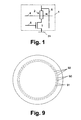
- An MRAM comprises a plurality of magnetoresistive memory units 1 arranged in an array.
- One such memory unit 1 is shown in Fig. 1 .
- Each memory unit 1 comprises a magnetoresistive memory element 2, a first intersection of a digit line 4 and a bit line 6, and a second intersection of the bit line 6 and a word line 8.
- the memory units 1 are coupled in series in columns by means of the bit lines 6 and coupled in series in rows by means of the digit lines 4 and word lines 8, thus forming the array.
- the magnetoresistive memory elements 2 used may for example, but not limited thereto, be magnetic tunnel junctions (MTJs).
- An MTJ memory element 2 is used by connecting it in a circuit such that electricity can flow vertically through the element 2 from one of the magnetic layers to the other.
- the MTJ unit 1 can be electrically represented by a resistor R in series with a switching element such as a transistor T, as shown in Fig. 1 .
- the size of the resistance of the resistor R depends on the orientation of the magnetic vectors of the free and pinned magnetic layers of the memory element 2.
- the MTJ element 2 has a relatively high resistance (HiRes) when the magnetic vectors point in opposite directions, and it has a relatively low resistance (LoRes) when the magnetic vectors point in the same direction.
- FIG. 2 A diagrammatic elevational view of a 2x2 array of prior art memory units is shown in Fig. 2 .
- an MRAM array comprising a plurality of MRAM units, orthogonal conductive lines 4, 6 pass under and over each bit or memory element 2, carrying current that produces a switching field.
- Each bit is designed so that it will not switch when current is applied to just one line, but will switch when current is flowing through both lines that cross at the selected bit (switching will occur only if the magnetic vector of the free layer is not in accordance with the direction of the switching field).
- Digit lines 4 and bit lines 6 are provided in an array of MTJ memory units 1, where the digit lines 4 travel along the rows of the array on one side of the memory elements 2, and the bit lines 6 travel down the columns of the array on the opposite side of the memory elements 2.
- the structure in Fig. 2 is partially inverted for clarity purposes: digit lines 4 physically run underneath the MTJ elements 2 (at that side of the MTJ elements 2 oriented towards the substrate in which the transistor T is provided), and bit lines 6 physically run over the MTJ elements 2 (at that side of the MTJ elements 2 oriented away from the substrate in which the transistor T is provided). However, if drawn that way, the bit lines 6 would obscure the magnetoresistive elements 2, which are the more relevant parts of the an MRAM.
- MTJ memory elements 2 are layered structures generally including, as represented in Fig. 2 , a non-magnetic conductor forming a lower electrical contact 22, a fixed or pinned magnetic layer 10, a dielectric barrier layer 14 positioned on the pinned layer 10, and a free magnetic layer 12 positioned on a dielectric barrier layer 14, with an upper contact 16 on the free magnetic layer 12.
- the pinned magnetic layer 10 and the free magnetic layer 12 may both be composed of e.g. NiFe, and the dielectric barrier layer 14 may e.g. be made of AlOx.
- the pinned layer 10 of magnetic material has a magnetic vector that always points in the same direction.
- the magnetic vector of the free layer 12 is free, but constrained by the physical size of the layer, to point in either of two directions: parallel or anti-parallel with the magnetization direction of the pinned layer 10.
- the memory element 2 is connected to the transistor T by means of an interconnect layer 16 and a plurality of metalization layers 18 and vias 20. There is a galvanic connection 22 between the memory element 2 and the bit line 6.
- the transistor T of each memory unit 1 is connected to a ground line 24.
- An MRAM array consisting of a 2-D matrix 30 of magnetic storage elements 32, 32a, 32b located at the intersections of two sets of orthogonal current lines, word lines 8 and bit lines 6, is schematically illustrated in Fig. 3 .
- the array represented has a limited size, but in practice much larger sizes are possible.
- required currents flow through selected digit lines 4 and bit lines 6 so that at their intersection a peak magnetic field is generated, sufficient to switch e.g. the polarization of the free layer 12 of the MTJ element 32a, so as to switch the resistance of the MTJ unit 32a from the LoRes (low resistance) state to the HiRes (high resistance) state or vice versa (depending on the direction of the current through the bit line 6).
- the switching element such as transistor T in the selected memory unit 1 (the memory unit at the intersection of the selected digit line 4 and the selected bit line 6) is in the cut-off state, for example by keeping the voltage on the word line 8 low (0 volt in case the switching element is a transistor T).
- the currents in the selected digit line 4 and the selected bit line 6 are such that together they provide a magnetic field able to change the direction of the magnetic vector of the free layer of the selected memory element, but the current in either strip by itself is not able to change the storage state. Therefore only the selected memory element 32a is written, not any of the other memory elements 32b on the same selected digit line 4 or bit line 6.
- two orthogonal current lines 4, 6 are used to create an in-plane magnetic field vector, whose amplitude is maximal at a selected bit 32a.
- both field components may be influencing other magnetic elements 32b along the selected current lines 4, 6 ( Fig. 3 ).
- This event is generally called 'half-select', and is responsible for the accelerated relaxation of (non-selected) magnetic bits 32b.
- the energy barrier against thermal relaxation of all bits 32b influenced by a half-select is lowered considerably. Therefore, for an embedded MRAM memory, in which read and write operations occur with similar high frequency, the accumulated half-select time will define the expected thermal relaxation time, i.e., for a reduced energy barrier.
- WORM write-few read-many
- this relaxation time was calculated for a 240 x 120 nm 2 elliptic MRAM element with a 4 nm NiFe free layer.
- a typical astroid curve is obtained (symbols O and X, calculated at 0 K), also called a Stoner-Wohlfarth astroid. This curve is contrasted with different stability criteria.
- the solid curves 40, 41, 42, 43, 44, 45 trace the boundaries of stability for a single idealized particle for magnetization pointing either left or right as a function of applied magnetic field.
- the axes of the plot correspond to the easy and hard axis field, i.e. parallel or perpendicular to the direction preferred by the crystalline anisotropy.
- the area within the different solid curves 40, 41, 42, 43, 44, 45 represent the fields which can be applied to non-selected bits in order to preserve thermal stability for times of respectively 1 second, 1 minute, 1 hour, 1 day, 1 month, and 1 year. It is to be noticed that a data retention specification of 10 15 read/write cycles corresponds to an effective time of ⁇ 3 1/2 months for a 10 nano-second half-select pulse time. This stability requirement results in a stable write field window as shown in the dark regions 50 in Fig. 5 .
- Each point in these dark regions 50 shows a combination of magnetic fields according to the easy axis and according to the hard axis, which can be used to write a memory element, and which are such that each magnetic field separately (according to the hard axis or according to the easy axis) is not sufficient to switch a memory element.
- thermal stability requirement is strongly affected by the switching field distribution resulting from variations in shape and geometry of the magnetic elements (lithography, edge roughness and micromagnetism), as well as from distributions in the generation of on-chip magnetic fields. Tolerances or margins have to be set to overcome these process variations. On the other hand, due to the exponential relationship, these small changes are very important in the thermal stability analysis, as can clearly be seen in Fig. 4 .
- a magnetic relaxation simulator is provided with an array of memory elements for storing data.
- the simulator may be used to estimate when the memory elements storing data need to be refreshed.
- the simulator may comprise reference magnetic elements or bits with a range of sizes smaller than the minimum size used for actual data storage. This is in order to reflect the statistical distribution in sizes and physical characteristics of the actual memory elements and associated field sources.
- an array of elements with different sizes may be included in order to obtain a more accurate impression of the thermal stability, which is a strong function of volume, and hence size for fixed layer thickness. By probing elements with different sizes, the decay can be monitored and adequate countermeasures can be taken. For the example given, this means that the MRAM does not only contain memory elements 2, but also an array of reference memory elements.
- a reference memory element or bit has dimensions such that its magnetization will relax in a shorter time than the minimum expected relaxation time of the storage elements 2 or bits. This can be such that either the area, or the aspect ratio, or both, of the reference elements is different from the area, or the aspect ratio, or both, of the actual memory elements.
- Probing of the magnetization, or thus of the stored content, of the reference elements or bits allows the detection of the probable onset of magnetization relaxation in the storage elements 2 or bits, therefore signaling that the re-writing (re-magnetizing) of the storage elements 2 or bits is necessary.
- Such a scheme can be organized over rows, columns, or sectors.
- test structure for the whole chip, one may check for a possible ambient influence like temperature or magnetic field, at regular intervals during operation, or e.g. when booting a system. Based on the output of the test, the whole memory can be declared to be corrupted, e.g. remagnetized in too high a field, or totally random in too high a temperature.
- the test structure can be a temperature and/or field monitoring unit by itself, or be combined with one. If a back-up is present, the memory can be re-set. In this case, it may be important to have back-ups at regular intervals. If the test points out that part of the memory is possibly corrupted, then (that part of) the memory can be rewritten.
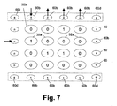
- Pre-set reference elements can be implemented in the memory array in various ways. Preferred embodiments include the possibility to check for half-select operations on both logic '0' and '1' states, as one of the currents, i.e. the bit current in line 6 in Fig. 3 , can be applied bi-directionally. One option would be to simply add extra rows 0 and/or M+1, and columns 0 and/or N+1, for an MxN memory block, as illustrated in the embodiment of Fig. 6 , wherein these extra rows and columns consist of reference memory elements 60, 60b, 60c, 60d with dimensions such that their magnetization will relax in a shorter time than the minimum expected relaxation time of the storage elements or bits 32, 32a, 32b. In the example given in Fig.
- the reference elements 60, 60b, 60c, 60d have a smaller area than the actual memory elements 32, 32a, 32b.
- a peak magnetic field is applied to memory element 32a
- a first partial magnetic field is applied to all memory elements 32b on the same row as target memory element 32a
- a second partial magnetic field is applied to all memory elements 32b on the same column as target memory element 32a.
- the first partial magnetic field is applied to reference element 60b
- the second partial magnetic field is applied to reference element 60c.
- the first and second partial magnetic fields are such that their combined effect generates a magnetic field, which is sufficient to switch memory element 32a, but each individual magnetic field is not sufficient to switch any of the memory elements 32b.
- the magnetization of the reference elements 60, 60b, 60c is probed according to a schedule that may be pre-programmed, or adapted, in accordance with the known physical properties of the magnetic elements or bits, the previous behavior of the simulator, a virtual simulator running within the data storage device, or a detailed virtual simulator running separate to the data storage device.
- a very simple schedule may dictate probing the reference elements after every write or read operation, or after a pre-defined number of write or read operations.
- thermal stability is mainly an issue during write operations, which is a very local operation, since at that moment only bits along the programming bit and digit lines have a lowered energy barrier against thermally-assisted switching.
- test elements on these lines are sufficient to monitor the possibility of unwanted switching in these neighboring elements. In this case, a positive test would result in rewriting all of the neighboring elements. In the case of e.g. a word-parallel writing strategy, this means that a whole memory block should be rewritten.
- test-cells with logic 0 and 1 value, in each row and/or column, as represented in Fig. 7 .
- the thermal stability test would be to compare both values in the selected lines after every write operation, or, e.g. statistically distributed in the matrix, over every few write operations. If the resistance difference ⁇ R between both states is too small, then either test-0 become test-1 or vice versa. In any case, one of the states is changed, which detects the likely onset of thermal relaxation in the matrix. It is to be noted that due to the different size, comparison to standard elements is not possible. Therefore, e.g. at the corners, specific standard elements for reference, which are not or hardly exposed to on-chip fields, can be pre-programmed.
- the bit status of the reference elements on the left and right can be checked. If they give an error, the word can be either read and compared with the initial data that is still available, or it can simply be rewritten. On the other hand, if any of the reference bits on the reference rows has changed its bit status, then the likely onset of thermal relaxation is detected, and the whole matrix can be read and rewritten, after first resetting all reference bits.
- test structures comprising pre-set elements can be implemented in the memory architecture.
- the sole requirement is that on-chip currents or magnetic fields are influencing the reference elements in a similar fashion as functional bits.
- test features can readily be implemented, based on the same idea, i.e. reference elements are added to detect the likely onset of thermal relaxation in the matrix.
- the magnetic relaxation simulator may also be virtual in form, comprising a predictive model programmed into a processing element within or associated with the data storage device.
- the processor may be a microprocessor or an embedded processor core.
- the processor may also be a programmable gate array such as a Programmable Logic Array (PLA) or a Programmable Array Logic (PAL) or a Field Programmable Gate Array (FPGA).
- PLA Programmable Logic Array
- PAL Programmable Array Logic
- FPGA Field Programmable Gate Array
- the simulation may be done by predicting the thermal relaxation of magnetic storage elements on the basis of an established relationship between the thermal relaxation of magnetic storage elements and physical processes that occur therein, such as magnetization switching due to writing of values.
- the model is of sufficient complexity to predict the actual behavior of a "hardware" simulator, i.e.
- a simulator with reference storage elements as described above. Obtaining that complexity may be dependent upon knowing the actual physical and operational characteristics of the storage magnetic elements or bits to a sufficient level of accuracy as initial input data for the model.
- the model may have to be structured in such a way as to simulate the physical processes that occur within a "hardware" simulator to a very high level of accuracy.
- Such a virtual simulator may require a large processing overhead, or extremely fast processing infrastructure in order to run in "real time”. Such requirements may be relaxed if a simplified model is used to simulate the "hardware" simulator with sufficient accuracy to be used in practice.
- an extremely accurate virtual simulator can be run "off-line", not in real time, and the results can be stored in the data storage device in such a way as to be accessible by the device in order to control the operation of the device.
- a virtual simulator can also be used in tandem with a hardware simulator within the data storage device.
- a further variation is to use a hardware simulator in combination with the results of a more complex virtual simulator, that have been stored in an accessible manner within the data storage device.
- a further embodiment of a simulator according to the present invention may for example be applied in hard disk based data storage systems.
- the write process in hard disk drives consists of magnetizing areas or domains 80, 80a, 80b, 80c, 80d along narrow circumferential tracks within the media with an externally applied magnetic field (see Fig. 8 ).
- the externally applied magnetic field may be generated by means of write head poles 81 and a write head coil 82.
- the direction of the magnetic field defines the magnetization of the domain 80, 80a, 80b, 80c, 80d to be written.
- the data to be written is encoded such that a transition 83 between two oppositely magnetized domains 80a, 80b corresponds to a first binary state, e.g.
- Hard disk drives make use of servo information embedded in special header sub-sections 90 of data found at the beginning of subdivisions of data known as sectors 91 (see Fig. 9 ). These headers 90 are used to assist in the following of tracks 92 by the flying head (not represented), the identification of the tracks 92 and also the identification of the sectors 91. Data files may be sub-divided between the physical sectors 91 found on the hard disk, or sectors 91 may contain several small data files.
- the magnetic relaxation simulator may be realized in the hard disk media platter by writing a reference pattern of bits into a pre-defined area on the disk. Such areas may be embedded within the headers 90 of each sector 91, or in a separate area on each track 92, or within a single pre-defined track 91.
- the pattern of bits is structured such that it contains a series of oppositely magnetized domains, possessing initially well defined magnetic volumes and boundaries.
- the magnetic volumes should be chosen such that they suffer from detectable magnetic relaxation over time scales shorter than that for the magnetic volume defined by the minimum distance between transitions in areas containing stored data.
- the reference bit pattern may consist of one or more equally sized magnetic volumes, or a range of magnetic volumes allowing a distribution of relaxation times to be probed.
- Magnetic relaxation within the reference pattern may proceed by the random, thermally induced reversal of the magnetization of individual grains within each magnetic volume. This may result in the magnetic volume becoming "demagnetized” via the initially written magnetic domain splitting into equal numbers of unstable small magnetic volumes. This would result in the media exhibiting a larger background noise during read-back from the reference bits. Additionally, grains close to the boundaries between domains (transitions) may be more prone to reversal due to the added influence of the larger demagnetizing field that exists close to transitions. This may lead to the transitions between domains becoming less well defined and eventually "self-erasing". This would result in the read-back signal from transitions becoming noisier and eventually in the transition becoming undetectable.
- the magnetic relaxation of the reference bits may be probed by monitoring the background signal to noise ratio from the reference pattern, monitoring the transition noise from the reference pattern, or monitoring when the transitions in the reference pattern become impossible to detect.
- the latter may be the preferred method as it allows individual transitions linked to pre-defined magnetic volumes of a certain size to be probed.
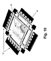
- An embodiment of the simulator according to the present invention may for example also be applied in probe based data storage devices.
- An example of a probe based system is shown in Fig. 10 .
- Such devices usually consist of an array 95 of probes manufactured using MEMS (micro-electromechanical systems) processes that are used to access data written into a separate media 96.
- MEMS micro-electromechanical systems
- the media 96 and probe array 95 move relative to each other in an XY raster pattern, actuated by actuators 97.
- Probe based data storage devices may use continuous media reading, writing and coding methods similar to those described for hard disk based systems. Probe based systems may also use media patterned into individual elements, these elements possessing magnetizations perpendicular to the plane of the media 96. Similar to hard disks, data is written by aligning the magnetization of the elements with an externally applied magnetic field possessing the appropriate polarization. A first binary value, e.g. "1”, may be represented by an element whose magnetization is aligned away from the media plane towards the probe array, and a second binary value, e.g. "0", by an element whose magnetization is aligned in the reverse direction.
- a first binary value e.g. "1”
- a second binary value e.g. "0”
- Reading is performed by detecting the direction of the magnetization of the individual magnetic elements via the interaction of an individual probe with an individual magnetic element. This may be done by detecting the direction of the stray magnetic field, which is directly related to the direction of the magnetization of the bit, emanating from the magnetic elements.
- Several methods exist by which the direction of the stray field can be probed including the use of GMR or TMR sensors mounted on the probes, or the monitoring of the deflection of a permanently magnetized probe when interacting with the stray magnetic field from an element.
- a magnetization relaxation simulator may be realized in a probe based data storage device incorporating patterned media 96 in the following way. During the media manufacturing process, arrays of equally sized elements are patterned in order to form individual bit locations for the storage of data. The simulator is realized by defining areas on the media 96 where an element or group of elements possess dimensions (magnetic volumes) smaller than those of the data storage elements. The size of the reference element(s) is such that their magnetization relaxes in a time shorter than that for the data elements. The magnetic relaxation of the reference element(s) is detected by comparing their magnetization at some pre-defined time, with their initial pre-defined magnetization. Any mismatch between the two will reveal that the magnetization in the reference element(s) has relaxed due to random thermal fluctuations and that the information stored in the data elements should be refreshed.
- Reference elements may be indexed to rows or columns of data elements, the reference magnetization being set at the time of writing information to the respective rows or columns. Thus the reference elements need not be located adjacent to their respective data elements, but do need to have their reference magnetizations set at the same time as any data is written.
- the reference magnetizations of a group of reference elements may be defined to form a certain pattern of elements with parallel and anti-parallel magnetizations.
- the reference elements may form groups of elements, each group containing elements with a distribution of sizes (magnetic volumes) and hence a distribution in magnetic relaxation times. By monitoring the progress of magnetization relaxation as a function of element size, predictive control of the refreshing of bit elements may be implemented.
Landscapes
- Engineering & Computer Science (AREA)
- Computer Hardware Design (AREA)
- Mram Or Spin Memory Techniques (AREA)
- Hall/Mr Elements (AREA)
- Semiconductor Memories (AREA)
- Investigating Or Analyzing Materials By The Use Of Magnetic Means (AREA)
- Magnetic Record Carriers (AREA)
- Recording Or Reproducing By Magnetic Means (AREA)
- Soft Magnetic Materials (AREA)
- Measurement And Recording Of Electrical Phenomena And Electrical Characteristics Of The Living Body (AREA)
Claims (13)
- Magnetische Speichervorrichtung enthaltend:ein Array (30) von magnetischen Speicherelementen (32, 32a, 32b) zur Datenspeicherung; und einen magnetischen Relaxationssimulator zum Simulieren und Vorhersagen des Onsets der thermischen Relaxation der magnetischen Speicherelemente (32, 32a, 32b),wobei die magnetische Speichervorrichtung betreibbar ist zum Auffrischen der magnetischen Speicherelemente in Reaktion auf den vorhergesagten Onset der thermischen Relaxation.
- Magnetische Speichervorrichtung nach Anspruch 1, wobei der Simulator mindestens ein Element oder ein Array von Elementen an magnetischen Referenzspeicherelementen (60, 60b, 60c, 60d) aufweist, zum Detektieren des Onsets der thermischen Relaxation der magnetischen Speicherelemente (32, 32a, 32b).
- Magnetische Speichervorrichtung gemäß Anspruch 2, wobei jedes Speicherelement (32, 32a, 32b) ein magnetisches Volumen aufweist, wobei die magnetischen Referenzspeicherelemente (60, 60b, 60c, 60d) ein magnetisches Volumen haben, welches kleiner ist als das minimale magnetische Volumen, welches für eine tatsächliche Datenspeicherung verwendet wird.
- Magnetische Speichervorrichtung gemäß Anspruch 3, wobei das magnetische Volumen eines Speicher- oder Referenzelements (60, 60b, 60c, 60d, 32, 32a, 32b) sich auf sein Aspektverhältnis bezieht.
- Magnetische Speichervorrichtung gemäß irgendeinem der Ansprüche 3 oder 4, wobei das magnetische Volumen eines Speicher- oder Referenzelements (60, 60b, 60c, 60d, 32, 32a, 32b) sich auf seine Fläche bezieht.
- Magnetische Speichervorrichtung gemäß irgendeinem der vorhergehenden Ansprüche, wobei der Simulator ein Prozessierelement aufweist, welches ein Vorhersagemodell der thermischen Relaxation von magnetischen Speicherelementen (32, 32a, 32b) enthält.
- Magnetische Speichervorrichtung gemäß irgendeinem der vorhergehenden Ansprüche, wobei der Speicher eine magnetische Datenspeichervorrichtung ist.
- Magnetische Speichervorrichtung gemäß irgendeinem der vorhergehenden Ansprüche, wobei die magnetischen Speicher- oder Referenzelemente (60, 60b, 60c, 60d, 32, 32a, 32b) enthalten sind innerhalb einer kontinuierlichen dünnen Schicht von magnetischem Material.
- Magnetische Speichervorrichtung gemäß irgendeinem der vorhergehenden Ansprüche, wobei die magnetischen Speicher- oder Referenzelemente (60, 60b, 60c, 60d, 32, 32a, 32b) definiert sind durch eine kontinuierliche dünne Schicht von magnetischem Material, die in einzelne Elemente strukturiert wurde.
- Magnetische Speichervorrichtung gemäß irgendeinem der vorhergehenden Ansprüche, wobei die magnetischen Speicher- oder Referenzelemente (60, 60b, 60c, 60d, 32, 32a, 32b) definiert sind durch Bilden der einzelnen magnetischen Elemente innerhalb einer vordefinierten strukturierten Struktur.
- Verfahren enthaltend:Bestimmen eines wahrscheinlichen Onsets der thermischen Relaxation in einer magnetischen Datenspeichervorrichtung durch Simulieren und Vorhersagen des Onsets der thermischen Relaxation von magnetischen Speicherelementen (32, 32a, 32b) der magnetischen Datenspeichervorrichtung; undAuffrischen der magnetischen Speicherelemente in Reaktion auf den vorhergesagten Onset der thermischen Relaxation.
- Verfahren gemäß Anspruch 11, wobei die magnetische Speichervorrichtung Datenspeicherelemente (32, 32a, 32b) und magnetische Referenzspeicherelemente (60, 60b, 60c, 60d) aufweist, das Verfahren enthaltend Vergleichen von magnetischen Zuständen von magnetischen Referenzspeicherelementen (60, 60b, 60c, 60d) als ein Maß für die thermische Stabilität von mindestens einem der magnetischen Referenzspeicherelemente (60, 60b, 60c, 60d) in der magnetischen Speichervorrichtung.
- Verfahren gemäß irgendeinem der Ansprüche 11 oder 12, das Verfahren enthaltend Vorhersagen der thermischen Relaxation von magnetischen Speicherelementen (32, 32a, 32b) auf der Basis von einer festgestellten Beziehung zwischen der thermischen Relaxation von magnetischen Speicherelementen (32, 32a, 32b) und physikalischen Prozessen, die daran auftreten.
Priority Applications (1)
| Application Number | Priority Date | Filing Date | Title |
|---|---|---|---|
| EP03758590A EP1568038B1 (de) | 2002-11-28 | 2003-11-06 | Verfahren und vorrichtung zum erkennen des beginns einer thermischen relaxation in magnetischen datenspeichern |
Applications Claiming Priority (4)
| Application Number | Priority Date | Filing Date | Title |
|---|---|---|---|
| EP02080007 | 2002-11-28 | ||
| EP02080007 | 2002-11-28 | ||
| EP03758590A EP1568038B1 (de) | 2002-11-28 | 2003-11-06 | Verfahren und vorrichtung zum erkennen des beginns einer thermischen relaxation in magnetischen datenspeichern |
| PCT/IB2003/005018 WO2004049343A1 (en) | 2002-11-28 | 2003-11-06 | A method and device to detect the likely onset of thermal relaxation in magnetic data storage devices |
Publications (2)
| Publication Number | Publication Date |
|---|---|
| EP1568038A1 EP1568038A1 (de) | 2005-08-31 |
| EP1568038B1 true EP1568038B1 (de) | 2011-01-26 |
Family
ID=32338130
Family Applications (1)
| Application Number | Title | Priority Date | Filing Date |
|---|---|---|---|
| EP03758590A Expired - Lifetime EP1568038B1 (de) | 2002-11-28 | 2003-11-06 | Verfahren und vorrichtung zum erkennen des beginns einer thermischen relaxation in magnetischen datenspeichern |
Country Status (10)
| Country | Link |
|---|---|
| US (1) | US8014192B2 (de) |
| EP (1) | EP1568038B1 (de) |
| JP (1) | JP2006511001A (de) |
| KR (1) | KR20050087808A (de) |
| CN (1) | CN1717744B (de) |
| AT (1) | ATE497241T1 (de) |
| AU (1) | AU2003274616A1 (de) |
| DE (1) | DE60335904D1 (de) |
| TW (1) | TW200415590A (de) |
| WO (1) | WO2004049343A1 (de) |
Families Citing this family (9)
| Publication number | Priority date | Publication date | Assignee | Title |
|---|---|---|---|---|
| WO2005096315A2 (en) | 2004-04-01 | 2005-10-13 | Koninklijke Philips Electronics N.V. | Thermally stable reference voltage generator for mram |
| TWI279798B (en) * | 2005-08-04 | 2007-04-21 | Ind Tech Res Inst | Magnetoresistive memory arrays |
| JP4945592B2 (ja) * | 2009-03-13 | 2012-06-06 | 株式会社東芝 | 半導体記憶装置 |
| US8374052B2 (en) | 2009-05-08 | 2013-02-12 | Samsung Electronics Co., Ltd. | Information storage devices using magnetic domain wall movement and methods of operating the same |
| US9170879B2 (en) * | 2009-06-24 | 2015-10-27 | Headway Technologies, Inc. | Method and apparatus for scrubbing accumulated data errors from a memory system |
| EP2891996A4 (de) * | 2012-08-30 | 2016-01-27 | Fujitsu Ltd | Simulationsprogramm, simulationsvorrichtung und simulationsverfahren für magnetmaterial |
| KR102152774B1 (ko) | 2013-03-07 | 2020-09-07 | 삼성전자 주식회사 | 반도체 소자 시뮬레이션 시스템 및 이를 이용한 시뮬레이션 방법 |
| KR102507269B1 (ko) | 2016-03-29 | 2023-03-07 | 삼성전자주식회사 | 생체 정보를 이용하여 보안성을 높일 수 있는 센서, 상기 센서를 포함하는 모바일 장치, 및 상기 모바일 장치의 인증 방법 |
| US10672832B2 (en) | 2017-11-08 | 2020-06-02 | Taiwan Semiconductor Manufacturing Co., Ltd. | Magnetic detection circuit, MRAM and operation method thereof |
Family Cites Families (8)
| Publication number | Priority date | Publication date | Assignee | Title |
|---|---|---|---|---|
| US5068826A (en) * | 1990-01-18 | 1991-11-26 | Microunity Systems Engineering | Hall effect semiconductor memory cell |
| US6166948A (en) * | 1999-09-03 | 2000-12-26 | International Business Machines Corporation | Magnetic memory array with magnetic tunnel junction memory cells having flux-closed free layers |
| US6185143B1 (en) | 2000-02-04 | 2001-02-06 | Hewlett-Packard Company | Magnetic random access memory (MRAM) device including differential sense amplifiers |
| JP4309075B2 (ja) * | 2000-07-27 | 2009-08-05 | 株式会社東芝 | 磁気記憶装置 |
| US6724674B2 (en) * | 2000-11-08 | 2004-04-20 | International Business Machines Corporation | Memory storage device with heating element |
| US6426907B1 (en) * | 2001-01-24 | 2002-07-30 | Infineon Technologies North America Corp. | Reference for MRAM cell |
| JP2002314048A (ja) * | 2001-04-18 | 2002-10-25 | Canon Inc | 強磁性体不揮発性メモリおよびそのリフレッシュ方法 |
| US6839271B1 (en) * | 2003-10-15 | 2005-01-04 | Hewlett-Packard Development Company, L.P. | Magnetic memory device |
-
2003
- 2003-11-06 KR KR1020057009561A patent/KR20050087808A/ko not_active Ceased
- 2003-11-06 DE DE60335904T patent/DE60335904D1/de not_active Expired - Lifetime
- 2003-11-06 US US10/536,291 patent/US8014192B2/en active Active
- 2003-11-06 AT AT03758590T patent/ATE497241T1/de not_active IP Right Cessation
- 2003-11-06 JP JP2004554755A patent/JP2006511001A/ja not_active Withdrawn
- 2003-11-06 EP EP03758590A patent/EP1568038B1/de not_active Expired - Lifetime
- 2003-11-06 CN CN200380104337.7A patent/CN1717744B/zh not_active Expired - Fee Related
- 2003-11-06 WO PCT/IB2003/005018 patent/WO2004049343A1/en not_active Ceased
- 2003-11-06 AU AU2003274616A patent/AU2003274616A1/en not_active Abandoned
- 2003-11-25 TW TW092133030A patent/TW200415590A/zh unknown
Also Published As
| Publication number | Publication date |
|---|---|
| DE60335904D1 (de) | 2011-03-10 |
| EP1568038A1 (de) | 2005-08-31 |
| US20060018148A1 (en) | 2006-01-26 |
| WO2004049343A1 (en) | 2004-06-10 |
| ATE497241T1 (de) | 2011-02-15 |
| JP2006511001A (ja) | 2006-03-30 |
| CN1717744B (zh) | 2012-09-26 |
| KR20050087808A (ko) | 2005-08-31 |
| CN1717744A (zh) | 2006-01-04 |
| TW200415590A (en) | 2004-08-16 |
| US8014192B2 (en) | 2011-09-06 |
| AU2003274616A1 (en) | 2004-06-18 |
Similar Documents
| Publication | Publication Date | Title |
|---|---|---|
| JP4896341B2 (ja) | 磁気ランダムアクセスメモリ及びその作動方法 | |
| Engel et al. | The science and technology of magnetoresistive tunneling memory | |
| CN1191586C (zh) | 存储单元装置及其作为磁性ram与联合存储器的应用 | |
| EP1061592A2 (de) | Magnetoresistives Element, und seine Verwendung als Speicherelement | |
| JP4660529B2 (ja) | 二重接合磁気メモリデバイスの読み出し方法および二重接合磁気メモリデバイスへの書き込み方法 | |
| US8817530B2 (en) | Data-masked analog and digital read for resistive memories | |
| US20080225584A1 (en) | Magnetic storage element responsive to spin polarized current | |
| EP1509922B1 (de) | Mram-zelle und speicherarchitektur mit maximalem lesesignal und reduzierter elektromagnetischer interferenz | |
| CN101751989B (zh) | 使用磁畴壁移动的信息存储装置及操作该装置的方法 | |
| US7102477B2 (en) | Magnetic element with switchable domain structure | |
| EP1568038B1 (de) | Verfahren und vorrichtung zum erkennen des beginns einer thermischen relaxation in magnetischen datenspeichern | |
| US7224634B2 (en) | Hardware security device for magnetic memory cells | |
| JP2009158789A (ja) | 電流磁気効果素子及び磁気センサ | |
| Pohm et al. | Bias field and end effects on the switching thresholds of" pseudo spin valve" memory cells | |
| US8659852B2 (en) | Write-once magentic junction memory array | |
| US7203088B2 (en) | Magnetoresistive random access memory and driving method thereof | |
| US20050094435A1 (en) | Increased magnetic stability devices suitable for use as sub-micron memories | |
| Åkerman | Magnetoresistive random access memory | |
| Dagotto | Brief introduction to giant magnetoresistance (GMR) | |
| EP1576615B1 (de) | Hardwaresicherheitseinrichtung für magnetspeicherzellen | |
| Åkerman | Random Access |
Legal Events
| Date | Code | Title | Description |
|---|---|---|---|
| PUAI | Public reference made under article 153(3) epc to a published international application that has entered the european phase |
Free format text: ORIGINAL CODE: 0009012 |
|
| 17P | Request for examination filed |
Effective date: 20050628 |
|
| AK | Designated contracting states |
Kind code of ref document: A1 Designated state(s): AT BE BG CH CY CZ DE DK EE ES FI FR GB GR HU IE IT LI LU MC NL PT RO SE SI SK TR |
|
| AX | Request for extension of the european patent |
Extension state: AL LT LV MK |
|
| DAX | Request for extension of the european patent (deleted) | ||
| 17Q | First examination report despatched |
Effective date: 20070628 |
|
| RAP1 | Party data changed (applicant data changed or rights of an application transferred) |
Owner name: NXP B.V. |
|
| GRAP | Despatch of communication of intention to grant a patent |
Free format text: ORIGINAL CODE: EPIDOSNIGR1 |
|
| GRAS | Grant fee paid |
Free format text: ORIGINAL CODE: EPIDOSNIGR3 |
|
| GRAA | (expected) grant |
Free format text: ORIGINAL CODE: 0009210 |
|
| AK | Designated contracting states |
Kind code of ref document: B1 Designated state(s): AT BE BG CH CY CZ DE DK EE ES FI FR GB GR HU IE IT LI LU MC NL PT RO SE SI SK TR |
|
| REG | Reference to a national code |
Ref country code: GB Ref legal event code: FG4D |
|
| REG | Reference to a national code |
Ref country code: CH Ref legal event code: EP |
|
| REG | Reference to a national code |
Ref country code: IE Ref legal event code: FG4D |
|
| REF | Corresponds to: |
Ref document number: 60335904 Country of ref document: DE Date of ref document: 20110310 Kind code of ref document: P |
|
| REG | Reference to a national code |
Ref country code: DE Ref legal event code: R096 Ref document number: 60335904 Country of ref document: DE Effective date: 20110310 |
|
| REG | Reference to a national code |
Ref country code: NL Ref legal event code: VDEP Effective date: 20110126 |
|
| PG25 | Lapsed in a contracting state [announced via postgrant information from national office to epo] |
Ref country code: GR Free format text: LAPSE BECAUSE OF FAILURE TO SUBMIT A TRANSLATION OF THE DESCRIPTION OR TO PAY THE FEE WITHIN THE PRESCRIBED TIME-LIMIT Effective date: 20110427 Ref country code: PT Free format text: LAPSE BECAUSE OF FAILURE TO SUBMIT A TRANSLATION OF THE DESCRIPTION OR TO PAY THE FEE WITHIN THE PRESCRIBED TIME-LIMIT Effective date: 20110526 Ref country code: SE Free format text: LAPSE BECAUSE OF FAILURE TO SUBMIT A TRANSLATION OF THE DESCRIPTION OR TO PAY THE FEE WITHIN THE PRESCRIBED TIME-LIMIT Effective date: 20110126 Ref country code: ES Free format text: LAPSE BECAUSE OF FAILURE TO SUBMIT A TRANSLATION OF THE DESCRIPTION OR TO PAY THE FEE WITHIN THE PRESCRIBED TIME-LIMIT Effective date: 20110507 |
|
| PG25 | Lapsed in a contracting state [announced via postgrant information from national office to epo] |
Ref country code: NL Free format text: LAPSE BECAUSE OF FAILURE TO SUBMIT A TRANSLATION OF THE DESCRIPTION OR TO PAY THE FEE WITHIN THE PRESCRIBED TIME-LIMIT Effective date: 20110126 Ref country code: SI Free format text: LAPSE BECAUSE OF FAILURE TO SUBMIT A TRANSLATION OF THE DESCRIPTION OR TO PAY THE FEE WITHIN THE PRESCRIBED TIME-LIMIT Effective date: 20110126 Ref country code: CY Free format text: LAPSE BECAUSE OF FAILURE TO SUBMIT A TRANSLATION OF THE DESCRIPTION OR TO PAY THE FEE WITHIN THE PRESCRIBED TIME-LIMIT Effective date: 20110126 Ref country code: AT Free format text: LAPSE BECAUSE OF FAILURE TO SUBMIT A TRANSLATION OF THE DESCRIPTION OR TO PAY THE FEE WITHIN THE PRESCRIBED TIME-LIMIT Effective date: 20110126 Ref country code: BE Free format text: LAPSE BECAUSE OF FAILURE TO SUBMIT A TRANSLATION OF THE DESCRIPTION OR TO PAY THE FEE WITHIN THE PRESCRIBED TIME-LIMIT Effective date: 20110126 Ref country code: FI Free format text: LAPSE BECAUSE OF FAILURE TO SUBMIT A TRANSLATION OF THE DESCRIPTION OR TO PAY THE FEE WITHIN THE PRESCRIBED TIME-LIMIT Effective date: 20110126 Ref country code: BG Free format text: LAPSE BECAUSE OF FAILURE TO SUBMIT A TRANSLATION OF THE DESCRIPTION OR TO PAY THE FEE WITHIN THE PRESCRIBED TIME-LIMIT Effective date: 20110426 |
|
| PG25 | Lapsed in a contracting state [announced via postgrant information from national office to epo] |
Ref country code: EE Free format text: LAPSE BECAUSE OF FAILURE TO SUBMIT A TRANSLATION OF THE DESCRIPTION OR TO PAY THE FEE WITHIN THE PRESCRIBED TIME-LIMIT Effective date: 20110126 Ref country code: DK Free format text: LAPSE BECAUSE OF FAILURE TO SUBMIT A TRANSLATION OF THE DESCRIPTION OR TO PAY THE FEE WITHIN THE PRESCRIBED TIME-LIMIT Effective date: 20110126 |
|
| PG25 | Lapsed in a contracting state [announced via postgrant information from national office to epo] |
Ref country code: RO Free format text: LAPSE BECAUSE OF FAILURE TO SUBMIT A TRANSLATION OF THE DESCRIPTION OR TO PAY THE FEE WITHIN THE PRESCRIBED TIME-LIMIT Effective date: 20110126 Ref country code: SK Free format text: LAPSE BECAUSE OF FAILURE TO SUBMIT A TRANSLATION OF THE DESCRIPTION OR TO PAY THE FEE WITHIN THE PRESCRIBED TIME-LIMIT Effective date: 20110126 Ref country code: CZ Free format text: LAPSE BECAUSE OF FAILURE TO SUBMIT A TRANSLATION OF THE DESCRIPTION OR TO PAY THE FEE WITHIN THE PRESCRIBED TIME-LIMIT Effective date: 20110126 |
|
| PLBE | No opposition filed within time limit |
Free format text: ORIGINAL CODE: 0009261 |
|
| STAA | Information on the status of an ep patent application or granted ep patent |
Free format text: STATUS: NO OPPOSITION FILED WITHIN TIME LIMIT |
|
| 26N | No opposition filed |
Effective date: 20111027 |
|
| REG | Reference to a national code |
Ref country code: DE Ref legal event code: R097 Ref document number: 60335904 Country of ref document: DE Effective date: 20111027 |
|
| PG25 | Lapsed in a contracting state [announced via postgrant information from national office to epo] |
Ref country code: IT Free format text: LAPSE BECAUSE OF FAILURE TO SUBMIT A TRANSLATION OF THE DESCRIPTION OR TO PAY THE FEE WITHIN THE PRESCRIBED TIME-LIMIT Effective date: 20110126 |
|
| REG | Reference to a national code |
Ref country code: GB Ref legal event code: 732E Free format text: REGISTERED BETWEEN 20120510 AND 20120516 |
|
| REG | Reference to a national code |
Ref country code: DE Ref legal event code: R081 Ref document number: 60335904 Country of ref document: DE Owner name: CROCUS TECHNOLOGY,INC.(N.D.GES.D.STAATES DELAW, US Free format text: FORMER OWNER: NXP B.V., EINDHOVEN, NL Effective date: 20120419 |
|
| PG25 | Lapsed in a contracting state [announced via postgrant information from national office to epo] |
Ref country code: MC Free format text: LAPSE BECAUSE OF NON-PAYMENT OF DUE FEES Effective date: 20111130 |
|
| REG | Reference to a national code |
Ref country code: CH Ref legal event code: PL |
|
| PG25 | Lapsed in a contracting state [announced via postgrant information from national office to epo] |
Ref country code: CH Free format text: LAPSE BECAUSE OF NON-PAYMENT OF DUE FEES Effective date: 20111130 Ref country code: LI Free format text: LAPSE BECAUSE OF NON-PAYMENT OF DUE FEES Effective date: 20111130 |
|
| REG | Reference to a national code |
Ref country code: IE Ref legal event code: MM4A |
|
| PG25 | Lapsed in a contracting state [announced via postgrant information from national office to epo] |
Ref country code: IE Free format text: LAPSE BECAUSE OF NON-PAYMENT OF DUE FEES Effective date: 20111106 |
|
| PG25 | Lapsed in a contracting state [announced via postgrant information from national office to epo] |
Ref country code: LU Free format text: LAPSE BECAUSE OF NON-PAYMENT OF DUE FEES Effective date: 20111106 |
|
| PG25 | Lapsed in a contracting state [announced via postgrant information from national office to epo] |
Ref country code: TR Free format text: LAPSE BECAUSE OF FAILURE TO SUBMIT A TRANSLATION OF THE DESCRIPTION OR TO PAY THE FEE WITHIN THE PRESCRIBED TIME-LIMIT Effective date: 20110126 |
|
| PG25 | Lapsed in a contracting state [announced via postgrant information from national office to epo] |
Ref country code: HU Free format text: LAPSE BECAUSE OF FAILURE TO SUBMIT A TRANSLATION OF THE DESCRIPTION OR TO PAY THE FEE WITHIN THE PRESCRIBED TIME-LIMIT Effective date: 20110126 |
|
| REG | Reference to a national code |
Ref country code: FR Ref legal event code: PLFP Year of fee payment: 13 |
|
| REG | Reference to a national code |
Ref country code: FR Ref legal event code: PLFP Year of fee payment: 14 |
|
| REG | Reference to a national code |
Ref country code: FR Ref legal event code: PLFP Year of fee payment: 15 |
|
| REG | Reference to a national code |
Ref country code: FR Ref legal event code: TP Owner name: CROCUS TECHNOLOGY INC., US Effective date: 20171221 |
|
| REG | Reference to a national code |
Ref country code: FR Ref legal event code: CA Effective date: 20180522 |
|
| REG | Reference to a national code |
Ref country code: FR Ref legal event code: PLFP Year of fee payment: 16 |
|
| PGFP | Annual fee paid to national office [announced via postgrant information from national office to epo] |
Ref country code: FR Payment date: 20221021 Year of fee payment: 20 |
|
| PGFP | Annual fee paid to national office [announced via postgrant information from national office to epo] |
Ref country code: GB Payment date: 20221021 Year of fee payment: 20 Ref country code: DE Payment date: 20221020 Year of fee payment: 20 |
|
| P01 | Opt-out of the competence of the unified patent court (upc) registered |
Effective date: 20230626 |
|
| REG | Reference to a national code |
Ref country code: DE Ref legal event code: R071 Ref document number: 60335904 Country of ref document: DE |
|
| REG | Reference to a national code |
Ref country code: GB Ref legal event code: PE20 Expiry date: 20231105 |
|
| PG25 | Lapsed in a contracting state [announced via postgrant information from national office to epo] |
Ref country code: GB Free format text: LAPSE BECAUSE OF EXPIRATION OF PROTECTION Effective date: 20231105 |
|
| PG25 | Lapsed in a contracting state [announced via postgrant information from national office to epo] |
Ref country code: GB Free format text: LAPSE BECAUSE OF EXPIRATION OF PROTECTION Effective date: 20231105 |