EP1569018A2 - Guide d'ondes polymère avec une couche favorisant l'adhésion - Google Patents
Guide d'ondes polymère avec une couche favorisant l'adhésion Download PDFInfo
- Publication number
- EP1569018A2 EP1569018A2 EP05101178A EP05101178A EP1569018A2 EP 1569018 A2 EP1569018 A2 EP 1569018A2 EP 05101178 A EP05101178 A EP 05101178A EP 05101178 A EP05101178 A EP 05101178A EP 1569018 A2 EP1569018 A2 EP 1569018A2
- Authority
- EP
- European Patent Office
- Prior art keywords
- waveguide
- oxide film
- glue
- sio
- cladding
- Prior art date
- Legal status (The legal status is an assumption and is not a legal conclusion. Google has not performed a legal analysis and makes no representation as to the accuracy of the status listed.)
- Withdrawn
Links
- 229920000642 polymer Polymers 0.000 title claims description 30
- 239000003292 glue Substances 0.000 claims abstract description 49
- 238000005253 cladding Methods 0.000 claims abstract description 41
- 239000013307 optical fiber Substances 0.000 claims abstract description 33
- VYPSYNLAJGMNEJ-UHFFFAOYSA-N Silicium dioxide Chemical group O=[Si]=O VYPSYNLAJGMNEJ-UHFFFAOYSA-N 0.000 claims abstract description 30
- 229910052814 silicon oxide Inorganic materials 0.000 claims abstract description 29
- 239000000203 mixture Substances 0.000 claims abstract description 9
- 239000000758 substrate Substances 0.000 claims description 31
- 229910052751 metal Inorganic materials 0.000 claims description 14
- 239000002184 metal Substances 0.000 claims description 14
- 239000000463 material Substances 0.000 claims description 7
- 229910052500 inorganic mineral Inorganic materials 0.000 claims description 6
- 239000011707 mineral Substances 0.000 claims description 6
- QVGXLLKOCUKJST-UHFFFAOYSA-N atomic oxygen Chemical compound [O] QVGXLLKOCUKJST-UHFFFAOYSA-N 0.000 claims description 2
- 239000001301 oxygen Substances 0.000 claims description 2
- 229910052760 oxygen Inorganic materials 0.000 claims description 2
- 239000000835 fiber Substances 0.000 abstract description 39
- 239000000853 adhesive Substances 0.000 abstract description 23
- 230000001070 adhesive effect Effects 0.000 abstract description 23
- 239000011347 resin Substances 0.000 abstract description 22
- 229920005989 resin Polymers 0.000 abstract description 22
- 125000004430 oxygen atom Chemical group O* 0.000 abstract description 11
- 239000011521 glass Substances 0.000 description 17
- 230000003287 optical effect Effects 0.000 description 11
- 238000004519 manufacturing process Methods 0.000 description 8
- 229910004794 SiO1.3 Inorganic materials 0.000 description 7
- 238000000034 method Methods 0.000 description 6
- 239000004033 plastic Substances 0.000 description 6
- 229920003023 plastic Polymers 0.000 description 6
- 238000004299 exfoliation Methods 0.000 description 5
- 239000000126 substance Substances 0.000 description 5
- XKRFYHLGVUSROY-UHFFFAOYSA-N Argon Chemical compound [Ar] XKRFYHLGVUSROY-UHFFFAOYSA-N 0.000 description 4
- 238000000151 deposition Methods 0.000 description 4
- 230000008021 deposition Effects 0.000 description 4
- 239000002987 primer (paints) Substances 0.000 description 4
- 238000004544 sputter deposition Methods 0.000 description 4
- 238000012360 testing method Methods 0.000 description 4
- 230000015556 catabolic process Effects 0.000 description 3
- 238000005229 chemical vapour deposition Methods 0.000 description 3
- 238000004891 communication Methods 0.000 description 3
- 238000006731 degradation reaction Methods 0.000 description 3
- 238000002329 infrared spectrum Methods 0.000 description 3
- 230000002093 peripheral effect Effects 0.000 description 3
- 229910052710 silicon Inorganic materials 0.000 description 3
- 229910008051 Si-OH Inorganic materials 0.000 description 2
- 229910006358 Si—OH Inorganic materials 0.000 description 2
- 238000005411 Van der Waals force Methods 0.000 description 2
- 229910052786 argon Inorganic materials 0.000 description 2
- 238000003491 array Methods 0.000 description 2
- 125000004429 atom Chemical group 0.000 description 2
- 230000008901 benefit Effects 0.000 description 2
- 239000011248 coating agent Substances 0.000 description 2
- 238000000576 coating method Methods 0.000 description 2
- 150000001875 compounds Chemical class 0.000 description 2
- 238000013016 damping Methods 0.000 description 2
- 238000001704 evaporation Methods 0.000 description 2
- 229910052739 hydrogen Inorganic materials 0.000 description 2
- 239000001257 hydrogen Substances 0.000 description 2
- 125000004435 hydrogen atom Chemical group [H]* 0.000 description 2
- 230000009545 invasion Effects 0.000 description 2
- 238000000016 photochemical curing Methods 0.000 description 2
- 229920003229 poly(methyl methacrylate) Polymers 0.000 description 2
- 239000004926 polymethyl methacrylate Substances 0.000 description 2
- 238000010008 shearing Methods 0.000 description 2
- 239000010703 silicon Substances 0.000 description 2
- 239000004925 Acrylic resin Substances 0.000 description 1
- FYYHWMGAXLPEAU-UHFFFAOYSA-N Magnesium Chemical compound [Mg] FYYHWMGAXLPEAU-UHFFFAOYSA-N 0.000 description 1
- 239000004642 Polyimide Substances 0.000 description 1
- 229910004738 SiO1 Inorganic materials 0.000 description 1
- 229910020389 SiO1.8 Inorganic materials 0.000 description 1
- 239000006087 Silane Coupling Agent Substances 0.000 description 1
- 125000002723 alicyclic group Chemical group 0.000 description 1
- 229910052782 aluminium Inorganic materials 0.000 description 1
- XAGFODPZIPBFFR-UHFFFAOYSA-N aluminium Chemical compound [Al] XAGFODPZIPBFFR-UHFFFAOYSA-N 0.000 description 1
- PNEYBMLMFCGWSK-UHFFFAOYSA-N aluminium oxide Inorganic materials [O-2].[O-2].[O-2].[Al+3].[Al+3] PNEYBMLMFCGWSK-UHFFFAOYSA-N 0.000 description 1
- 230000005540 biological transmission Effects 0.000 description 1
- 238000010538 cationic polymerization reaction Methods 0.000 description 1
- 239000000470 constituent Substances 0.000 description 1
- 229910052593 corundum Inorganic materials 0.000 description 1
- 230000008878 coupling Effects 0.000 description 1
- 238000010168 coupling process Methods 0.000 description 1
- 238000005859 coupling reaction Methods 0.000 description 1
- 230000003247 decreasing effect Effects 0.000 description 1
- 230000006866 deterioration Effects 0.000 description 1
- 239000003822 epoxy resin Substances 0.000 description 1
- 238000005530 etching Methods 0.000 description 1
- 238000002474 experimental method Methods 0.000 description 1
- 239000003365 glass fiber Substances 0.000 description 1
- 238000013007 heat curing Methods 0.000 description 1
- 238000007731 hot pressing Methods 0.000 description 1
- 238000001746 injection moulding Methods 0.000 description 1
- 229910052749 magnesium Inorganic materials 0.000 description 1
- 239000011777 magnesium Substances 0.000 description 1
- 239000005304 optical glass Substances 0.000 description 1
- 239000011368 organic material Substances 0.000 description 1
- TWNQGVIAIRXVLR-UHFFFAOYSA-N oxo(oxoalumanyloxy)alumane Chemical compound O=[Al]O[Al]=O TWNQGVIAIRXVLR-UHFFFAOYSA-N 0.000 description 1
- 150000003071 polychlorinated biphenyls Chemical group 0.000 description 1
- 229920000647 polyepoxide Polymers 0.000 description 1
- 229920001721 polyimide Polymers 0.000 description 1
- 239000003505 polymerization initiator Substances 0.000 description 1
- 239000013615 primer Substances 0.000 description 1
- 230000005855 radiation Effects 0.000 description 1
- 238000005510 radiation hardening Methods 0.000 description 1
- 239000007870 radical polymerization initiator Substances 0.000 description 1
- 229920006395 saturated elastomer Polymers 0.000 description 1
- 238000007789 sealing Methods 0.000 description 1
- XLYOFNOQVPJJNP-UHFFFAOYSA-N water Substances O XLYOFNOQVPJJNP-UHFFFAOYSA-N 0.000 description 1
- 230000037303 wrinkles Effects 0.000 description 1
- 229910001845 yogo sapphire Inorganic materials 0.000 description 1
Images


Classifications
-
- C—CHEMISTRY; METALLURGY
- C12—BIOCHEMISTRY; BEER; SPIRITS; WINE; VINEGAR; MICROBIOLOGY; ENZYMOLOGY; MUTATION OR GENETIC ENGINEERING
- C12M—APPARATUS FOR ENZYMOLOGY OR MICROBIOLOGY; APPARATUS FOR CULTURING MICROORGANISMS FOR PRODUCING BIOMASS, FOR GROWING CELLS OR FOR OBTAINING FERMENTATION OR METABOLIC PRODUCTS, i.e. BIOREACTORS OR FERMENTERS
- C12M37/00—Means for sterilizing, maintaining sterile conditions or avoiding chemical or biological contamination
-
- G—PHYSICS
- G02—OPTICS
- G02B—OPTICAL ELEMENTS, SYSTEMS OR APPARATUS
- G02B6/00—Light guides; Structural details of arrangements comprising light guides and other optical elements, e.g. couplings
- G02B6/10—Light guides; Structural details of arrangements comprising light guides and other optical elements, e.g. couplings of the optical waveguide type
- G02B6/12—Light guides; Structural details of arrangements comprising light guides and other optical elements, e.g. couplings of the optical waveguide type of the integrated circuit kind
- G02B6/122—Basic optical elements, e.g. light-guiding paths
- G02B6/1221—Basic optical elements, e.g. light-guiding paths made from organic materials
-
- G—PHYSICS
- G02—OPTICS
- G02B—OPTICAL ELEMENTS, SYSTEMS OR APPARATUS
- G02B6/00—Light guides; Structural details of arrangements comprising light guides and other optical elements, e.g. couplings
- G02B6/24—Coupling light guides
- G02B6/26—Optical coupling means
- G02B6/30—Optical coupling means for use between fibre and thin-film device
-
- G—PHYSICS
- G02—OPTICS
- G02B—OPTICAL ELEMENTS, SYSTEMS OR APPARATUS
- G02B6/00—Light guides; Structural details of arrangements comprising light guides and other optical elements, e.g. couplings
- G02B6/24—Coupling light guides
- G02B6/255—Splicing of light guides, e.g. by fusion or bonding
-
- G—PHYSICS
- G02—OPTICS
- G02B—OPTICAL ELEMENTS, SYSTEMS OR APPARATUS
- G02B6/00—Light guides; Structural details of arrangements comprising light guides and other optical elements, e.g. couplings
- G02B6/24—Coupling light guides
- G02B6/42—Coupling light guides with opto-electronic elements
- G02B6/4201—Packages, e.g. shape, construction, internal or external details
- G02B6/4219—Mechanical fixtures for holding or positioning the elements relative to each other in the couplings; Alignment methods for the elements, e.g. measuring or observing methods especially used therefor
- G02B6/4236—Fixing or mounting methods of the aligned elements
- G02B6/4239—Adhesive bonding; Encapsulation with polymer material
Definitions
- the invention relates generally to waveguide equipment and a polymer waveguide for optical communications.
- waveguide equipment In a connected portion or an end portion of an optical fiber cable for optical communications, waveguide equipment is used to connect the end of one optical fiber cable to, for example, another optical fiber cable, a light projection device, a photo detector, etc. So, it is requested that such waveguide equipment can be produced with low cost and be suitable for a mass production, as the use of the optical communication, which can transmit large capacity data with high-speed, has increased in recent years.
- a polymer waveguide using a high molecular compound (polymer) is suggested for the waveguide.
- the waveguide equipment is assembled by integrating the polymer waveguide with the optical fiber made of glass or polymer, an end surface of the polymer waveguide is integrated with an end surface of the fiber guide which holds the optical fiber using high molecular glue.
- the optical fiber or the optical fiber arrays are made of silica glass. So, adhesion is high between the glue and the optical fiber or the optical fiber arrays. This is because glass has many OH radicals and has high affinity with glue; so the glue is spread on the surface of the glass and bonds with the OH radicals on the surface of glass by hydrogen bond or van der Waals forces. And, if UV hardening glue is applied on a silane coupling agent on the glass, adhesion can be improved by a chemical bond. But, adhesion between the polymer waveguide and the glue is not stronger than that between the glass and the glue.
- FIG. 1 is a schematic cross-sectional view of the prior art that improved reliability of the adhesive strength.
- an optical fiber 12 is held to an optical fiber guide 11 and couples to a core 14 in a waveguide 13 optically.
- An end of the fiber guide 11 bonds with an end surface of the waveguide 13 using glue 15.
- the glue 15 is applied to an outer peripheral portion of the bonding surface between the fiber guide 11 and the waveguide 13, and it is hardened. As a result, exfoliation at the bonding surface is prevented between the fiber guide 11 and the waveguide 13.
- SiO 2 film is disposed on the surface of the glue 15 applied to the outer peripheral portion of the bonding surface, so an invasion of the moisture is prevented to the adhesive surface.
- Embodiments of the present invention improve the adhesive strength between the polymer waveguide and the optical fiber, and provide waveguide equipment which has a high reliability for moisture and temperature change.
- waveguide equipment comprises a polymer waveguide having a core and cladding, and an optical fiber which is connected to an end surface of the polymer waveguide with glue and which is optically connected with the core, wherein an oxide film formed between at least one end surface of the polymer waveguide or the optical fiber and the glue.
- a polymer waveguide comprises a core and a cladding of the polymer waveguide being formed on a substrate made of mineral matter materials, wherein an oxide film formed between at least one surface faced each other of the substrate or the cladding, and the surface of the cladding and the substrate connected via the oxide film with glue.
- a polymer waveguide comprises the polymer waveguide having a core and cladding, wherein an oxide film formed on the polymer waveguide and a metal film formed on the oxide film.
- FIG. 1 is a schematic cross-sectional view of the prior art.
- FIG. 2 is a perspective view of waveguide equipment in accordance with one embodiment of the present invention.
- FIG. 3 is an exploded perspective view of the waveguide equipment shown in FIG. 2.
- FIG. 4 is a perspective view of the waveguide formed an oxide film on an end surface.
- FIG. 5 is a longitudinal cross-sectional view of the waveguide equipment shown in FIG. 2.
- FIG. 6A and 6B are figures showing a bonding state between a SiO2 film and a glue.
- FIG. 7A and 7B are figures showing a bonding state between a SiOx film and a glue.
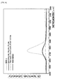
- FIG. 8 is a figure to show measured IR spectrum nearby Si-OH bonding in a sample formed of a SiO1.3 oxide film and various SiO2 oxide films.
- FIG. 9 shows an attenuation rate of the optical intensity of two kinds of samples, one kind of which is formed with several kinds of silicon oxide films on an end surface and one kind of which is not formed with an oxide film (prior art), and exposed high temperature high humidity environment for about 200 hours.
- FIG. 10 is a perspective view showing an embodiment of a waveguide in accordance with the present invention.
- FIG. 11 is a cross-sectional view showing an embodiment of the present invention.
- FIG. 12 is a cross-sectional view showing an embodiment of the present invention.
- FIG. 13B is a cross-sectional view of a waveguide used for an embodiment of the present invention and FIG. 13A is a figure to show a manufacturing process of the waveguide.
- FIG. 14B is a cross-sectional view of a waveguide used for an embodiment of the present invention and FIG. 14A is a figure to show a manufacturing process of the waveguide.
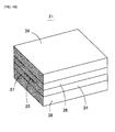
- FIG. 2 is a perspective view of waveguide equipment 20 in accordance with one embodiment of the present invention.
- FIG. 3 is an exploded perspective view of the waveguide equipment 20.
- the waveguide equipment 20 is formed by a single mode waveguide 21 and fiber guides 22, 23 for I/O port connected with both sides of the waveguide 21.
- the waveguide 21 is formed a under cladding 24, a core 25, and an over cladding 26.
- the under cladding 24 is made of transparent resin of the high refractive index and has a concave groove on a part of the top surface.
- the core 25 is formed by burying in the concave groove transparent resin with a higher refractive index than the under cladding 24.
- the width and height of the core 25 is about 6 ⁇ m in the case of the single mode waveguide.
- the transparent resin of the under cladding 24 and the over cladding 26 can be different transparent resin, but it is desirable to use the same resin.
- the ultraviolet radiation hardening type transparent resin is desirable as the resin to form the over and under cladding 26, 24 and the core 25, but the heat curing type transparent resin can also be used.
- PMMA polymethylmethacrylate
- photo-PCB photo-curing type polychlorinated biphenyl
- alicyclic epoxy resin photosensitive cationic polymerization initiator, acrylate resin (containing Si and F), photosensitive free-radical polymerization initiator, and fluoridated polyimide
- a reproduction method with a stamper is preferable to form the under cladding 24, but hot pressing, etching, and injection molding can be used to form the under cladding 24.
- a lot of the waveguide 21 is produced on a glass wafer at one time in a mass production, which improves productivity.
- the many optical waveguides 21 produced on the wafer are cut by dicing methods, and they are split into a piece of the waveguide 21. At this time, the end surface of each waveguide 21 is ground, and both end surfaces of the core 25 exposed may be finished smoothly.
- an oxide film 27 is layered on the entire surface of both end sides of the waveguide 21 by sputtering method, evaporation method, ordinary temperature CVD method, or photo-CVD method.
- a SiO x film is layered on the end surface of the waveguide 21 as the oxide film 27 by sputtering method using silicon.
- a sputtering condition of this case uses argon plasma and SiO x having x value as desired (for example, SiO1 .3).
- the arrival pressure force is 3 ⁇ 10-6 Torr.
- the deposition pressure force is 5 ⁇ 10-3 Torr.
- the flow rate of argon is 20 sccm.
- the high frequency output power is 0.2 kW.
- the deposition time is two minutes.
- the film thickness of the oxide film 27 was 1000 ⁇ .
- molecules consisting of the oxide film 27 arrive at the end surface of the waveguide 21 with kinetic energy by the sputtering method and the evaporation method. So, the molecules are bonded with more OH radicals by ionic bonding or chemical bonding at the end surface of the waveguide 21. As a result, the exfoliative strength between the waveguide 21 and the oxide film 27 can be raised as compared to glue applied on the end surface of the waveguide directly.
- Silicon oxide film for the oxide film 27 is preferable, but the transparent oxide film such as even aluminum, magnesium, or SiON are preferable if the coupling efficiency between the optical fiber and the waveguide 21 does not become decreased.
- the oxide film in which the number of oxygen atoms is less than the most stable stoichiometric composition is desirable.
- the film that has a smaller ratio of an oxygen atom than Al 2 O 3 is preferable as the aluminum oxide film.
- the thickness of the oxide film 27 is thinner than 4000 ⁇ . That is because it prevents degradation of an optical transmission rate in the oxide film 27 and crack outbreak by internal stress of the oxide film 27.
- the thickness of oxide film 27 is thicker than 500 ⁇ . That is because it prevents water or steam from getting into the waveguide 21 through the oxide film 27.
- the oxide film 27 be layered by a cold temperature grown method of less than 200 degrees Celsius in order to not make the waveguide 21 deteriorate because it is a deposition on the resin of the waveguide 27 that the oxide film 27 is layered.
- a substrate temperature in a deposition equipment should be kept not more than 100 degrees Celsius when the oxide film is layered more than 2000 ⁇ to prevent cracks. So, the quality of the oxide film can be improved.
- the fiber guide 22 is made from a substrate 30, which is made of glass or plastic and is formed of plural of V-grooves 29 on a top surface and a fiber weight 31.
- a tape core 28A is torn off the coating of the end and exposes plural optical fibers 32 composed of a core and a cladding.
- Each optical fiber 32 is held in position in each V-groove 29 of the substrate 30 by the fiber weight 31 with the glue put on the optical fiber 32.
- Fiber weight 31 presses onto each optical fiber 32 so that the substrate 30 and the fiber weight 31 are integrated.
- the fiber guide 23 is made from a substrate 34, which is made in glass or plastic and is formed of a V-groove 33 on a top surface and a fiber weight 35.
- a tape core 28B is torn off the coating of the end and exposes an optical fiber 36 composed of a core and a cladding.
- the optical fiber 36 is held in position in the V-groove 33 of the substrate 34 by the fiber weight 35 with the glue put on the optical fiber 36.
- Fiber weight 35 presses onto the optical fiber 36 so that the substrate 34 and the fiber weight 35 are integrated.
- the optical fibers 32, 36 can be preferably made of either glass fiber or plastic fiber.
- FIG. 5 is a sectional view to show the waveguide equipment 20 assembled by bonding the fiber guide 22, 23 to both ends of the waveguide 21.
- glue 37 is applied between the oxide film 27 formed by both end sides of the waveguide 21 and fiber guide 22, 23.
- the waveguide 21 and the fiber guide 22, 23 are integrated with the glue 37.
- Primer coating may be put on the surface of oxide film 27 to improve adhesion with the oxide film 27 and the glue 37.
- the adhesion between the oxide film 27 and the glue 37 improves and the adhesion between the oxide film 27 and the waveguide 21 also improves. So, the adhesive strength improves between the waveguide 21 and the fiber guide 22, 23.
- the SiO 2 that has a stable composition is used as the oxide film 27, the exfoliative strength between the oxide film 27 and the glue 37 becomes lower and the exfoliative strength between the oxide film 27 and the waveguide 21 also becomes lower. So, the adhesive strength becomes lower between the waveguide 21 and the fiber guide 22, 23.
- the exfoliative strength between the oxide film 27 and the glue 37 can be improved and the exfoliative strength between the oxide film 27 and the waveguide 21 can be improved.
- the adhesive strength can be made higher between the waveguide 21 and the fiber guide 22, 23.
- the adhesive strength improves when an oxide film 27 that has a composition ratio of an oxygen atom which is smaller is formed on the end face of the waveguide 21.
- SiO 2 is formed as the oxide film 27 on the resin surface of the waveguide 21, that resin and the oxide film 27 are bonded because the OH radicals of the resin surface of the waveguide 21 and of the oxide film 27 bond chemically.
- SiO 2 is a stable composition and bonding of each atom is saturated. Thus, there is less excess binding residue in SiO 2 .
- SiO 2 and the resin bond chemically through an oxygen atom included in the OH radicals on the resin surface of waveguide 21, but the exfoliative strength is low between the waveguide 21 and the oxide film 27 for lack of binding residue with chemical bond.
- the bonding between the glue 37 and the oxide film 27 is also the same way. As shown in FIG. 6A, there is less excess binding residue in SiO 2 . So, as shown in FIG. 6B, there is less binding residue for chemical binding between SiO 2 and the glue 37 through an oxygen atom included in the OH radicals on the surface of the glue 37. Therefore, the exfoliative strength is also low between the glue 37 and the oxide film 27.
- the bonding state is unstable for unsaturated bonding by lack of an oxygen atom in SiO x (1 ⁇ x ⁇ 1.5). Therefore, many OH radicals appear on the surface of SiO x because an atmospheric H atom is bonded to SiO x , the oxide film 27. As a result, the OH radicals in SiO x react to the OH radicals in the waveguide 21 as follows. OH - +OH - ⁇ O 2 - +H 2 O
- the exfoliative strength between the waveguide 21 and the oxide film 27 can be improved by using SiO x (1 ⁇ x ⁇ 1.5) as the oxide film 27.
- the bonding between the glue 37 and the oxide film 27 is also the same way.
- the bonding state of the oxide film 27 is unstable for unsaturated bonding by lack of an oxygen atom. Therefore, as shown in FIG. 7A, many OH radicals appear on the surface of SiO x because an atmospheric H atom is bonded to SiO x , the oxide film 27.
- the OH radicals in SiO x react to the OH radicals in the glue 37 and these many OH radicals bond chemically through O atoms. So, the exfoliative strength between the glue 37 and the oxide film 27 can be improved by using SiO x (1 ⁇ x ⁇ 1.5) as the oxide film 27.
- both the exfoliative strength between the oxide film 27 and the waveguide 21 and the exfoliative strength between the oxide film 27 and the glue 37 can be improved by using SiO x (1 ⁇ x ⁇ 1.5) as the oxide film 27. Furthermore, the adhesive strength between the waveguide 21 and the glue 37 can be improved.
- FIG. 8 shows an IR spectrum intensity nearby Si-OH bonding measured with samples of SiO 1.3 , sputtered oxide film (SiO 2 ), thermal oxidized SiO 2 film, and NSG (SiO 2 by the CVD method).
- a horizontal axis shows a wavelength and vertical axis shows the IR spectrum intensity.
- This figure also shows that the number of OH radicals increase and the exfoliative strength between the resin and the oxide film are higher as the value of the vertical axis becomes larger.
- the OH radicals hardly appear in SiO 2 , but that several times the OH radicals appear in SiO 1.3 .
- SiO x (1 ⁇ x ⁇ 1.5) film is smaller than that of SiO 2 film.
- internal stress of SiO 1.3 is 1/5 compared with SiO 2 film.
- SiO 2 film was completely damaged when a sample consisting of polymer waveguide formed on a glass substrate, SiO 2 film formed thereupon, and a glass substrate bonded thereupon, was exposed for 20 hours to high temperature and high humidity condition.
- SiO 1.3 film was not damaged as only some wrinkles occurred to the oxide film when a sample consisting of polymer waveguide formed on a glass substrate, SiO 1.3 film formed thereupon, and a glass substrate bonded thereupon, was exposed for 20 hours to high temperature and high humidity condition. Therefore, the waveguide equipment 20 which is hard to deteriorate under high temperature and high humidity condition, superior in reliability, and having high adhesive strength can be produced using SiO x (1 ⁇ x ⁇ 1.5) as oxide film 27.
- FIG. 9 two kinds of samples of the waveguide 21 in which the resin is easy to change its characteristic at high temperature and high humidity condition are presented.
- one sample is formed silicon oxide film on the end surface of the waveguide 21 and another sample has no silicon oxide film.
- an attenuation rate of signal strength is measured using an optical signal of 1.31 ⁇ m wavelength and 1.55 ⁇ m wavelength.
- FIG. 9 As can be seen from FIG. 9, the SiO 1.8 film sample, the SiO 2 film sample, and no oxide film sample showed large damping by deterioration. But the SiO 1.3 film sample showed very small damping.
- a break down test was done with the waveguide equipment 20 produced above.
- the waveguide equipment 20 was put into a PCT (Pressure Cooker Testing machine) at the break down test. As a result, it is made sure that adhesive strength was kept without damaging the oxide film 27 which was formed on the end of the waveguide 21 even after more than 50 hours of testing.
- the exemplary waveguide was single mode, but a multimode waveguide that has the same structure can be made using the same production method.
- FIG. 10 is a perspective view to show an embodiment of waveguide 21.
- the waveguide 21 comprises the under cladding 24, the core 25 and over cladding 26.
- the waveguide 21 which has the under cladding 24, the core 25 and the over cladding 26 may be put between a bottom substrate 38 and an upper substrate 39 made of mineral matter materials.
- the bottom substrate 38 and the upper substrate 39 should be used as the glass substrates which are mineral matter materials.
- a quartz glass or an optical glass may be used as a glass substrate.
- the oxide film 27 is formed on the end surface of the waveguide 21 made of organic materials and mineral matter materials.
- the end surface of the waveguide 21 formed oxide film 27 and the fiber guide 22 and 23 are adhered with the glue 37.
- the SiO 2 film is formed as the oxide film 27
- the oxide film 27 is damaged after exposed in high temperature and high humidity condition for a long time.
- SiO x (1 ⁇ x ⁇ 1.5) film is formed as the oxide film 27, the internal stress of oxide film 27 shrink and the oxide film 27 is not damaged after exposed in high temperature and high humidity condition for a long time.
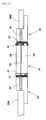
- FIG. 11 is a sectional view showing an embodiment of the present embodiment.
- the oxide film 27 is formed on an end surface of the connection side in the fiber guide 22 and 23. And the end surface of the fiber guide 22, 23 and the end surface of the waveguide 21 are adhered with the glue 37.
- the fiber guide 22, 23 is made of plastic and the optical fiber 32, 36 is also made of plastic. So, the adhesive strength is not enough when the glue is applied directly. Thus, the adhesive strength between the waveguide 21 and the fiber guide 22, 23 can be made higher by forming the oxide film at the end of the fiber guide 22, 23 and improving the adhesion between the fiber guide 22, 23 and the glue 37.
- the moisture which is a factor to make the adhesive strength with the glue 37 deteriorate may invade the glue 37 through the optical fiber 32, 36.
- the oxide film 27 intercepts the moisture by forming on the end surface of the fiber guide 22, 23 and sealing the end surface of the optical fiber 32, 36. Therefore, it is hard for moisture to reach the glue 37 and degradation of the adhesive strength by moisture can be prevented.
- FIG. 12 is a sectional view showing an embodiment of the present embodiment.
- the oxide film 27 is formed on both end surfaces of waveguide 21 and of the fiber guide 22, 23. And it is bonded with the glue 37 between the oxide film 27 of waveguide 21 and the oxide film 27 of the fiber guide 22, 23. Therefore, even if both the waveguide 21 and the fiber guide 22, 23 are made of plastic, the adhesive strength between the waveguide 21 and the fiber guide 22, 23 can be raised by improving the adhesion between the glue 37 and the waveguide 21, the fiber guide 22, 23.
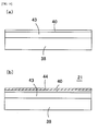
- FIG. 13B is sectional view of the waveguide 21 used an embodiment of the present invention.
- FIG. 13A shows the manufacturing process of the waveguide 21.
- an oxide film 40 such as SiO x (1 ⁇ x ⁇ 2) is formed on the bottom substrate 38 made of silicon and primer 41 is applied thereupon.
- Over cladding 26 that buries the core 25 is formed on an under surface of the upper substrate 39 made of glass.
- resin 42 for the under cladding is dropped on the primer 41.
- the resin 42 pushed from above by the upper substrate 39 is spread out between the primer 41 and the over cladding 26, and make rigid by UV radiations.
- the cladding 24 is formed.
- FIG. 13A shows the manufacturing process of the waveguide 21.
- an oxide film 40 such as SiO x (1 ⁇ x ⁇ 2) is formed on the bottom substrate 38 made of silicon and primer 41 is applied thereupon.
- Over cladding 26 that buries the core 25 is formed on an under surface of the upper substrate 39 made of glass.
- resin 42 for the under cladding
- the adhesive strength between the under cladding 24 and the bottom substrate 38 can be improved because the oxide film 40 is formed. So, it is hard for exfoliation to occur between the under cladding 24 and the bottom substrate 38 under a high temperature and a high humidity condition.
- FIG. 14B is a sectional view of the waveguide 21 used in an embodiment of the present invention.
- FIG. 14A shows the manufacturing process of the waveguide 21.
- the waveguide layer 43 which comprises the under cladding 24, the core 25, and the over cladding 26 is formed on the bottom substrate 38 made of glass.
- the oxide film 40 such as SiO x (1 ⁇ x ⁇ 2) is formed on the waveguide layer 43.
- a metal film 44 is formed on the oxide film 40 as an electrode by sputter.
- the waveguide 21 shown in FIG. 14B is obtained.
- the adhesive strength between the waveguide layer 43 and the metal film 44 can be improved because the oxide film 40 is formed. So, it is hard for exfoliation of the metal film 44 to occur under a high temperature and a high humidity condition. Especially, in the metal film 44, it is easy for exfoliation of the metal film 44 to occur because chipping of the substrate and turning up of the metal film occur during the dicing process of the waveguide 21.
- the adhesive strength of the metal film 44 at the dicing process can be improved because the metal film 44 is formed on the oxide film 40. If the metal film 44 is used as the electrode, bonding wires may be bonded on the metal film 44. In such instances, the shearing stress can be added to the metal film 44, but the shearing strength can be done more than 5 times by forming the metal film 44 on the oxide film 40.
- the waveguide equipment is coupled to an optical fiber on both sides of the waveguide.
- an optical transceiver such as a photo detector or a light projection device
- various kinds of forms such as an optical coupler, a WDM coupler, a VOA (a variable optical attenuator), an optical switch, and a multimode waveguide device may be used.
Landscapes
- Physics & Mathematics (AREA)
- Engineering & Computer Science (AREA)
- Optics & Photonics (AREA)
- General Physics & Mathematics (AREA)
- Life Sciences & Earth Sciences (AREA)
- Health & Medical Sciences (AREA)
- Organic Chemistry (AREA)
- Microelectronics & Electronic Packaging (AREA)
- Bioinformatics & Cheminformatics (AREA)
- Wood Science & Technology (AREA)
- Zoology (AREA)
- Chemical & Material Sciences (AREA)
- Biomedical Technology (AREA)
- General Engineering & Computer Science (AREA)
- General Health & Medical Sciences (AREA)
- Genetics & Genomics (AREA)
- Biochemistry (AREA)
- Sustainable Development (AREA)
- Microbiology (AREA)
- Biotechnology (AREA)
- Molecular Biology (AREA)
- Optical Integrated Circuits (AREA)
- Optical Couplings Of Light Guides (AREA)
Applications Claiming Priority (2)
| Application Number | Priority Date | Filing Date | Title |
|---|---|---|---|
| JP2004039970 | 2004-02-17 | ||
| JP2004039970A JP2005234025A (ja) | 2004-02-17 | 2004-02-17 | 光導波路装置 |
Publications (2)
| Publication Number | Publication Date |
|---|---|
| EP1569018A2 true EP1569018A2 (fr) | 2005-08-31 |
| EP1569018A3 EP1569018A3 (fr) | 2005-09-07 |
Family
ID=34747406
Family Applications (1)
| Application Number | Title | Priority Date | Filing Date |
|---|---|---|---|
| EP05101178A Withdrawn EP1569018A3 (fr) | 2004-02-17 | 2005-02-17 | Guide d'ondes polymère avec une couche favorisant l'adhésion |
Country Status (5)
| Country | Link |
|---|---|
| US (1) | US20050180696A1 (fr) |
| EP (1) | EP1569018A3 (fr) |
| JP (1) | JP2005234025A (fr) |
| KR (1) | KR100655025B1 (fr) |
| CN (1) | CN1301415C (fr) |
Families Citing this family (10)
| Publication number | Priority date | Publication date | Assignee | Title |
|---|---|---|---|---|
| JP2007072007A (ja) * | 2005-09-05 | 2007-03-22 | Sony Corp | 光導波路モジュール |
| JP4963375B2 (ja) * | 2005-11-02 | 2012-06-27 | 富士フイルム株式会社 | 光デバイス、光学部材及びライトガイド |
| KR101016546B1 (ko) * | 2007-01-18 | 2011-02-24 | 오무론 가부시키가이샤 | 광전송 모듈 및 전자 기기 |
| US9243784B2 (en) | 2012-12-20 | 2016-01-26 | International Business Machines Corporation | Semiconductor photonic package |
| US9400356B2 (en) | 2013-03-14 | 2016-07-26 | International Business Machines Corporation | Fiber pigtail with integrated lid |
| CN110108383A (zh) * | 2018-02-01 | 2019-08-09 | 桂林电子科技大学 | 基于长f-p腔光纤白光干涉型高温高灵敏度温度传感器 |
| JP2019215405A (ja) * | 2018-06-11 | 2019-12-19 | 日本電信電話株式会社 | 光ファイバ接続部品および光デバイスの作製方法 |
| CN108897105B (zh) * | 2018-07-31 | 2020-06-19 | 苏州易锐光电科技有限公司 | 应用于激光器器件的单透镜耦合方法 |
| WO2021247842A1 (fr) * | 2020-06-03 | 2021-12-09 | Commscope Technologies Llc | Dispositif d'alignement optique pour fibres nues comprenant une évacuation de l'air avec du gel |
| CN113311541A (zh) * | 2021-06-24 | 2021-08-27 | 四川梓冠光电科技有限公司 | 光开关、微电子机械系统及光开关安装方法 |
Citations (2)
| Publication number | Priority date | Publication date | Assignee | Title |
|---|---|---|---|---|
| EP0446672A1 (fr) * | 1990-03-16 | 1991-09-18 | International Business Machines Corporation | Guides d'onde optique polymérique et leur fabrication |
| EP1357405A1 (fr) * | 2001-01-31 | 2003-10-29 | Zeon Corporation | Plaque guide optique et unite d'eclairage |
Family Cites Families (9)
| Publication number | Priority date | Publication date | Assignee | Title |
|---|---|---|---|---|
| US4364731A (en) * | 1981-01-29 | 1982-12-21 | Board Of Regents, The University Of Texas System | Methods for producing adhesive bonds between substrate and polymer employing an intermediate oxide layer |
| US5589280A (en) * | 1993-02-05 | 1996-12-31 | Southwall Technologies Inc. | Metal on plastic films with adhesion-promoting layer |
| JP2000162460A (ja) * | 1998-11-27 | 2000-06-16 | Sharp Corp | 有機光導波路およびその製造方法並びにそれを用いた光学部品 |
| JP3774598B2 (ja) * | 1999-09-30 | 2006-05-17 | 株式会社日立製作所 | ポリマ導波路基板の製造方法およびポリマ導波路基板 |
| CA2387806A1 (fr) * | 2000-08-17 | 2002-02-21 | Koichiro Nakamura | Composition adhesive et dispositif optique l'utilisant |
| EP1399312A4 (fr) * | 2001-01-29 | 2004-08-04 | Honeywell Int Inc | Construction optique a haute reflexion robuste |
| US6614965B2 (en) * | 2001-05-11 | 2003-09-02 | Lightcross, Inc. | Efficient coupling of optical fiber to optical component |
| TW575745B (en) * | 2001-10-24 | 2004-02-11 | Hitachi Ltd | Optical waveguide member and optical module |
| US6841263B2 (en) * | 2002-05-03 | 2005-01-11 | The John Hopkins University | Method of adhering a solid polymer to a substrate and resulting article |
-
2004
- 2004-02-17 JP JP2004039970A patent/JP2005234025A/ja active Pending
-
2005
- 2005-01-31 KR KR1020050008441A patent/KR100655025B1/ko not_active Expired - Fee Related
- 2005-02-16 US US11/059,592 patent/US20050180696A1/en not_active Abandoned
- 2005-02-16 CN CNB2005100077396A patent/CN1301415C/zh not_active Expired - Fee Related
- 2005-02-17 EP EP05101178A patent/EP1569018A3/fr not_active Withdrawn
Patent Citations (2)
| Publication number | Priority date | Publication date | Assignee | Title |
|---|---|---|---|---|
| EP0446672A1 (fr) * | 1990-03-16 | 1991-09-18 | International Business Machines Corporation | Guides d'onde optique polymérique et leur fabrication |
| EP1357405A1 (fr) * | 2001-01-31 | 2003-10-29 | Zeon Corporation | Plaque guide optique et unite d'eclairage |
Also Published As
| Publication number | Publication date |
|---|---|
| KR100655025B1 (ko) | 2006-12-06 |
| US20050180696A1 (en) | 2005-08-18 |
| EP1569018A3 (fr) | 2005-09-07 |
| CN1657986A (zh) | 2005-08-24 |
| JP2005234025A (ja) | 2005-09-02 |
| KR20050082157A (ko) | 2005-08-22 |
| CN1301415C (zh) | 2007-02-21 |
Similar Documents
| Publication | Publication Date | Title |
|---|---|---|
| US7995875B2 (en) | Mirror-embedded optical waveguide and fabrication method of same | |
| EP0636909B1 (fr) | Module à guide d'ondes optique et son procédé de fabrication | |
| EP0634679B1 (fr) | Structure de couplage pour fibres optiques et guides d'ondes optiques | |
| CN1423753A (zh) | 无热化的光波导集成器件 | |
| US7492995B2 (en) | Optical element combination structure and optical fiber structure | |
| EP1569018A2 (fr) | Guide d'ondes polymère avec une couche favorisant l'adhésion | |
| US6553170B2 (en) | Method and system for a combination of high boron and low boron BPSG top clad fabrication process for a planar lightwave circuit | |
| JP4067504B2 (ja) | 光導波路及びその製造方法 | |
| EP0484011A2 (fr) | Emballage de composants optiques en silicium | |
| US6377732B1 (en) | Planar waveguide devices and fiber attachment | |
| US20060204197A1 (en) | Optical waveguide and method for preparing the same | |
| WO2008126653A1 (fr) | Procédé de fabrication d'un substrat de guide d'ondes pour montage à une surface optique | |
| US10338325B1 (en) | Nanofiller in an optical interface | |
| CN100432723C (zh) | 光学元件耦合结构体及光纤结构体 | |
| US5345545A (en) | Optical fiber device | |
| EP1356324A2 (fr) | Circuits integres optiques | |
| JP3440090B1 (ja) | 光通信部品、積層型光通信モジュール、およびその製造方法 | |
| US20060003484A1 (en) | Using deuterated source gasses to fabricate low loss GeSiON SiON waveguides | |
| US20030103726A1 (en) | Optical device | |
| US6670210B2 (en) | Optical waveguide with layered core and methods of manufacture thereof | |
| JP2009139474A (ja) | 光導波回路チップ | |
| JP2007183467A (ja) | ミラー付光導波路及びその製造方法 | |
| KR100393622B1 (ko) | 평면 도파로 소자 모듈 | |
| JP2003270504A (ja) | 光通信部品、積層型光通信モジュールの製造方法 | |
| JPH07172867A (ja) | 酸化シリコン膜光学素子及びその製造方法 |
Legal Events
| Date | Code | Title | Description |
|---|---|---|---|
| PUAI | Public reference made under article 153(3) epc to a published international application that has entered the european phase |
Free format text: ORIGINAL CODE: 0009012 |
|
| PUAL | Search report despatched |
Free format text: ORIGINAL CODE: 0009013 |
|
| AK | Designated contracting states |
Kind code of ref document: A2 Designated state(s): AT BE BG CH CY CZ DE DK EE ES FI FR GB GR HU IE IS IT LI LT LU MC NL PL PT RO SE SI SK TR |
|
| AX | Request for extension of the european patent |
Extension state: AL BA HR LV MK YU |
|
| AK | Designated contracting states |
Kind code of ref document: A3 Designated state(s): AT BE BG CH CY CZ DE DK EE ES FI FR GB GR HU IE IS IT LI LT LU MC NL PL PT RO SE SI SK TR |
|
| AX | Request for extension of the european patent |
Extension state: AL BA HR LV MK YU |
|
| 17P | Request for examination filed |
Effective date: 20051011 |
|
| AKX | Designation fees paid |
Designated state(s): AT BE BG CH CY CZ DE DK EE ES FI FR GB GR HU IE IS IT LI LT LU MC NL PL PT RO SE SI SK TR |
|
| 17Q | First examination report despatched |
Effective date: 20060224 |
|
| STAA | Information on the status of an ep patent application or granted ep patent |
Free format text: STATUS: THE APPLICATION IS DEEMED TO BE WITHDRAWN |
|
| 18D | Application deemed to be withdrawn |
Effective date: 20081004 |