JP4963375B2 - 光デバイス、光学部材及びライトガイド - Google Patents
光デバイス、光学部材及びライトガイド Download PDFInfo
- Publication number
- JP4963375B2 JP4963375B2 JP2006155613A JP2006155613A JP4963375B2 JP 4963375 B2 JP4963375 B2 JP 4963375B2 JP 2006155613 A JP2006155613 A JP 2006155613A JP 2006155613 A JP2006155613 A JP 2006155613A JP 4963375 B2 JP4963375 B2 JP 4963375B2
- Authority
- JP
- Japan
- Prior art keywords
- optical member
- optical
- film
- light
- protective medium
- Prior art date
- Legal status (The legal status is an assumption and is not a legal conclusion. Google has not performed a legal analysis and makes no representation as to the accuracy of the status listed.)
- Active
Links
Images


Classifications
-
- G—PHYSICS
- G02—OPTICS
- G02B—OPTICAL ELEMENTS, SYSTEMS OR APPARATUS
- G02B6/00—Light guides; Structural details of arrangements comprising light guides and other optical elements, e.g. couplings
- G02B6/24—Coupling light guides
-
- G—PHYSICS
- G02—OPTICS
- G02B—OPTICAL ELEMENTS, SYSTEMS OR APPARATUS
- G02B6/00—Light guides; Structural details of arrangements comprising light guides and other optical elements, e.g. couplings
- G02B6/24—Coupling light guides
- G02B6/26—Optical coupling means
- G02B6/262—Optical details of coupling light into, or out of, or between fibre ends, e.g. special fibre end shapes or associated optical elements
-
- G—PHYSICS
- G02—OPTICS
- G02B—OPTICAL ELEMENTS, SYSTEMS OR APPARATUS
- G02B6/00—Light guides; Structural details of arrangements comprising light guides and other optical elements, e.g. couplings
- G02B6/24—Coupling light guides
- G02B6/255—Splicing of light guides, e.g. by fusion or bonding
-
- G—PHYSICS
- G02—OPTICS
- G02B—OPTICAL ELEMENTS, SYSTEMS OR APPARATUS
- G02B6/00—Light guides; Structural details of arrangements comprising light guides and other optical elements, e.g. couplings
- G02B6/24—Coupling light guides
- G02B6/26—Optical coupling means
- G02B6/32—Optical coupling means having lens focusing means positioned between opposed fibre ends
-
- G—PHYSICS
- G02—OPTICS
- G02B—OPTICAL ELEMENTS, SYSTEMS OR APPARATUS
- G02B6/00—Light guides; Structural details of arrangements comprising light guides and other optical elements, e.g. couplings
- G02B6/24—Coupling light guides
- G02B6/36—Mechanical coupling means
-
- G—PHYSICS
- G02—OPTICS
- G02B—OPTICAL ELEMENTS, SYSTEMS OR APPARATUS
- G02B6/00—Light guides; Structural details of arrangements comprising light guides and other optical elements, e.g. couplings
- G02B6/24—Coupling light guides
- G02B6/42—Coupling light guides with opto-electronic elements
- G02B6/4201—Packages, e.g. shape, construction, internal or external details
- G02B6/4204—Packages, e.g. shape, construction, internal or external details the coupling comprising intermediate optical elements, e.g. lenses, holograms
- G02B6/421—Packages, e.g. shape, construction, internal or external details the coupling comprising intermediate optical elements, e.g. lenses, holograms the intermediate optical component consisting of a short length of fibre, e.g. fibre stub
Landscapes
- Physics & Mathematics (AREA)
- General Physics & Mathematics (AREA)
- Optics & Photonics (AREA)
- Engineering & Computer Science (AREA)
- Plasma & Fusion (AREA)
- Optical Couplings Of Light Guides (AREA)
- Mechanical Coupling Of Light Guides (AREA)
Description
また、前記第1の光学部材の出射端及び/又は前記第2の光学部材の入射端にUVクリーニングが施されていることとしてもよい。
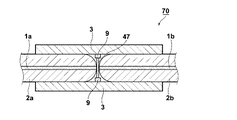
図1は本実施の形態の実施例1における光デバイス10、20の断面図である。光デバイス10は、光ファイバ(光学部材、ライトガイド)1a、1bと、フェルール2a、2bと、スリーブ(保持部材)3等によって構成される。フェルール2aの貫通孔には光ファイバ1aの一端が挿入され、フェルール2bの貫通孔には光ファイバ1bの一端が挿入される。また、スリーブ3に挿入される側のフェルール2の端部は半球面状に研磨される。
d1×N=(λ/2)×n ・・・(1)
(但し、nは1以上の整数)
であることが望ましい。
d2×N=(λ/4)×n ・・・(2)
(但し、nは1以上の整数)
を満足することが望ましい。一方、膜体42aと42bの膜厚がそれぞれ異なり、且つ膜体42aと42bが異種材料によって構成されており、屈折率も異なる場合、膜体42aの膜厚をd2a、屈折率をNa、膜体42bの膜厚をd2b、屈折率をNbとしたとき、光の発振波長λとの関係は、
(d2a×Na)+(d2b×Nb)=(λ/2)×n ・・・(3)
を満足することが望ましい。
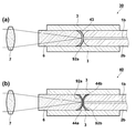
図3は、実施例2における光デバイス30の断面図を示した図である。光デバイス30のように、光導波路のないガラス等の透明部材6と光ファイバ1bを膜体43を介在させてスリーブ3に挿入して固定し、光学的に当接させてもよい。図3(a)に示すように、レンズ7に照射された光は透明部材6の端面92aに結合されて入射される。端面92aに結合された光は膜体43を介して光ファイバ1bの入射端から入射される。尚、膜体43は単層膜、多層膜の何れでもよく、材質、膜厚等は実施例1に記載したものと同様である。また、効果においても実施例1と同様の効果を奏する。また、図3(b)に示す光デバイス40ように、透明部材6の端面92aとフェルール2bの端面92bのそれぞれに膜体44a、44bが成膜されてもよい。
図5は、実施例3における光デバイス70及び80の断面図の一例を示した図である。まず図5(a)に示す光デバイス70について説明する。同図のように、貫通孔に光ファイバ1aが挿入されたフェルール2aの端面91aに膜51、52の順に2層以上の多層膜を成膜させてもよい。
2a、3b フェルール
3 スリーブ
41〜46 膜体
47 保護媒体
Claims (18)
- 入射された光を出射端から出射する第1の光学部材と、該第1の光学部材の出射端から出射された光を該出射端に対向する入射端から入射する第2の光学部材とからなる光デバイスにおいて、
前記第1の光学部材の出射端と前記第2の光学部材の入射端の間に、前記第1の光学部材と前記第2の光学部材の接着を抑止する保護媒体が配置され、前記第1の光学部材の出射端と前記保護媒体、また該保護媒体と前記第2の光学部材の入射端とがそれぞれ当接して配置され、
前記保護媒体が、前記第1の光学部材の出射端に成膜された膜体及び前記第2の光学部材の入射端に成膜された膜体から成り、前記第1の光学部材の出射端及び前記第2の光学部材の入射端に成膜された前記膜体の互いに当接する面が互いに異なる物質によって構成されることを特徴とする光デバイス。 - 入射された光を出射端から出射する第1の光学部材と、該第1の光学部材の出射端から出射された光を該出射端に対向する入射端から入射する第2の光学部材とからなる光デバイスにおいて、
前記第1の光学部材の出射端と前記第2の光学部材の入射端の間に、保護媒体が配置され、前記第1の光学部材の出射端と前記保護媒体、また該保護媒体と前記第2の光学部材の入射端とがそれぞれ当接して配置され、
前記保護媒体は、前記第1の光学部材と前記第2の光学部材とを500[g重]の荷重で該保護媒体と当接させ、後に離間させても、前記出射端と前記入射端を再使用可能な状態に維持する透明な保護媒体であり、
前記保護媒体が、前記第1の光学部材の出射端に成膜された膜体及び前記第2の光学部材の入射端に成膜された膜体から成り、前記第1の光学部材の出射端及び前記第2の光学部材の入射端に成膜された前記膜体の互いに当接する面が互いに異なる物質によって構成されることを特徴とする光デバイス。 - 前記荷重が、1[kg重]であることを特徴とする請求項2に記載の光デバイス。
- 前記膜体が多層膜であり、
前記第1の光学部材の出射端に成膜された前記多層膜の最上層膜と前記第2の光学部材の入射端に成膜された前記多層膜の最上層膜とが、互いに異なる物質によって構成される膜体であり、
前記第1の光学部材の出射端に成膜された前記多層膜の最上層膜と前記第2の光学部材の入射端に成膜された前記多層膜の最上層膜との当接部における密着性より、前記各多層膜を構成する膜同士の密着性、及び前記各多層膜の最下層膜と前記各光学部材との密着性の方が高いことを特徴とする請求項1〜3の何れか一項に記載の光デバイス。 - 前記保護媒体の屈折率と前記保護媒体の光導波方向に対する厚さの積が、λ/2の整数倍(但し、λ=前記光の発振波長)であることを特徴とする請求項1〜4の何れか一項に記載の光デバイス。
- 光導波方向に対する前記保護媒体の厚さが、λ/2未満であることを特徴とする請求項1〜4の何れか一項に記載の光デバイス。
- 前記保護媒体は、前記第1の光学部材の出射端から出射する光を前記第2の光学部材の入射端へ低損失で通過させるものであることを特徴とする請求項6に記載の光デバイス。
- 前記保護媒体が、フッ化物を含むものであることを特徴とする請求項7に記載の光デバイス。
- 前記保護媒体が、YF3、LiF、MgF2、NaF、LaF3、BaF2、CaF2及びAlF3からなる群から選ばれるものであることを特徴とする請求項8に記載の光デバイス。
- 前記多層膜の最上層膜が、フッ化物を含むものであることを特徴とする請求項4に記載の光デバイス。
- 前記フッ化物が、Siを含まないものであることを特徴とする請求項10に記載の光デバイス。
- 前記多層膜の最上層膜が、YF3、LiF、MgF2、NaF、LaF3、BaF2、CaF2及びAlF3からなる群から選ばれるものであることを特徴とする請求項10又は11に記載の光デバイス。
- 前記多層膜の最上層膜より下層の膜が、Siを含まない酸化膜であることを特徴とする請求項4及び10〜12の何れか一項に記載の光デバイス。
- 前記第1の光学部材に入射される光が、短波長領域の光であることを特徴とする請求項1〜13の何れか一項に記載の光デバイス。
- 前記第1の光学部材に入射される光の発振波長が、190[nm]〜530[nm]であることを特徴とする請求項14に記載の光デバイス。
- 前記第1の光学部材の出射端及び/又は前記第2の光学部材の入射端にUVクリーニングが施されていることを特徴とする請求項1〜15の何れか一項に記載の光デバイス。
- 前記第1の光学部材及び前記第2の光学部材の少なくとも一方がライトガイドであることを特徴とする請求項1〜16の何れか一項に記載の光デバイス。
- 前記ライトガイドは光ファイバであることを特徴とする請求項17に記載の光デバイス。
Priority Applications (5)
| Application Number | Priority Date | Filing Date | Title |
|---|---|---|---|
| JP2006155613A JP4963375B2 (ja) | 2005-11-02 | 2006-06-05 | 光デバイス、光学部材及びライトガイド |
| CN200610130898XA CN1982931B (zh) | 2005-11-02 | 2006-11-01 | 光学设备、光学部件及光导管 |
| TW095140343A TWI422884B (zh) | 2005-11-02 | 2006-11-01 | 具有經由保護中間物與光學構件連接的光學裝置 |
| US11/591,560 US7653275B2 (en) | 2005-11-02 | 2006-11-02 | Optical device having connections with optical members through protective medium |
| KR1020060108007A KR101258160B1 (ko) | 2005-11-02 | 2006-11-02 | 보호 매체를 통해 광학 부재와 접속되는 광 디바이스 |
Applications Claiming Priority (5)
| Application Number | Priority Date | Filing Date | Title |
|---|---|---|---|
| JP2005319226 | 2005-11-02 | ||
| JP2005319226 | 2005-11-02 | ||
| JP2006090100 | 2006-03-29 | ||
| JP2006090100 | 2006-03-29 | ||
| JP2006155613A JP4963375B2 (ja) | 2005-11-02 | 2006-06-05 | 光デバイス、光学部材及びライトガイド |
Publications (2)
| Publication Number | Publication Date |
|---|---|
| JP2007293228A JP2007293228A (ja) | 2007-11-08 |
| JP4963375B2 true JP4963375B2 (ja) | 2012-06-27 |
Family
ID=38173578
Family Applications (1)
| Application Number | Title | Priority Date | Filing Date |
|---|---|---|---|
| JP2006155613A Active JP4963375B2 (ja) | 2005-11-02 | 2006-06-05 | 光デバイス、光学部材及びライトガイド |
Country Status (5)
| Country | Link |
|---|---|
| US (1) | US7653275B2 (ja) |
| JP (1) | JP4963375B2 (ja) |
| KR (1) | KR101258160B1 (ja) |
| CN (1) | CN1982931B (ja) |
| TW (1) | TWI422884B (ja) |
Families Citing this family (5)
| Publication number | Priority date | Publication date | Assignee | Title |
|---|---|---|---|---|
| US10267999B2 (en) * | 2014-03-31 | 2019-04-23 | Koninklijke Philips N.V. | Optical connector for sterile applications |
| TWM540290U (zh) * | 2016-12-30 | 2017-04-21 | Luxnet Corp | 提升耦光效率的光通訊模組 |
| CA3084730A1 (en) * | 2017-12-12 | 2019-06-20 | Alcon Inc. | Thermally robust laser probe assembly |
| JPWO2020144909A1 (ja) * | 2019-01-08 | 2021-10-14 | 日本電信電話株式会社 | 光コネクタおよびその製造方法 |
| KR102835467B1 (ko) * | 2022-12-12 | 2025-07-18 | 주식회사 에이티솔루션 | 광섬유 케이블 커넥터 |
Family Cites Families (23)
| Publication number | Priority date | Publication date | Assignee | Title |
|---|---|---|---|---|
| JPS59218405A (ja) * | 1983-05-27 | 1984-12-08 | Sumitomo Electric Ind Ltd | 光エネルギ−伝送用フアイバ− |
| US4738497A (en) * | 1984-10-05 | 1988-04-19 | Matsushita Electric Industrial Co., Ltd. | Antireflection film |
| US5157461A (en) * | 1990-06-14 | 1992-10-20 | Smiths Industries Aerospace & Defense Systems Inc. | Interface configuration for rate sensor apparatus |
| US5308656A (en) * | 1991-07-16 | 1994-05-03 | Adc Telecommunications, Inc. | Electroformed mask and use therefore |
| JPH05181040A (ja) | 1991-12-28 | 1993-07-23 | Nec Corp | 光コネクタとその製造方法 |
| GB9326429D0 (en) * | 1993-12-24 | 1994-02-23 | Bt & D Technologies Ltd | An optical device and method of making the same |
| AU3484695A (en) * | 1994-09-16 | 1996-03-29 | Toray Industries, Inc. | Wide band optical fiber, optical fiber core wire and optical fiber cord |
| JPH09221342A (ja) | 1996-02-09 | 1997-08-26 | Nikon Corp | 光学部材の接着方法、及び、これを用いて接着された光学部品 |
| JP3530951B2 (ja) * | 1996-03-29 | 2004-05-24 | 株式会社日立コミュニケーションテクノロジー | 光ファイバ、光増幅器および光伝送システム |
| US6589650B1 (en) * | 2000-08-07 | 2003-07-08 | 3M Innovative Properties Company | Microscope cover slip materials |
| US6203208B1 (en) * | 1998-11-05 | 2001-03-20 | Illinois Tool Works Inc. | Fiber optic lighting system connector coupling medium |
| JP2000266939A (ja) * | 1999-03-12 | 2000-09-29 | Japan Aviation Electronics Industry Ltd | 光ファイバコネクタ |
| JP2001166179A (ja) * | 1999-12-03 | 2001-06-22 | Sumitomo Electric Ind Ltd | 光コネクタの組立方法及び光コネクタの組立工具 |
| US7036998B2 (en) * | 2001-05-17 | 2006-05-02 | Sumitomo Electric Industries, Ltd. | Optical part, optical module sleeve, optical receiving module, optical communication module, and method of making optical part |
| JP2003287655A (ja) * | 2002-03-27 | 2003-10-10 | Ntt Afty Corp | 光コネクタ型波長フィルタ |
| JP2003289655A (ja) * | 2002-03-27 | 2003-10-10 | Honda Motor Co Ltd | かご型回転子 |
| JP2004206068A (ja) * | 2002-10-29 | 2004-07-22 | Kyocera Corp | 光ファイバ及びその加工方法 |
| JP3929405B2 (ja) * | 2003-01-06 | 2007-06-13 | 信越ポリマー株式会社 | 光ファイバの接続装置 |
| JP2004252424A (ja) * | 2003-01-31 | 2004-09-09 | Fuji Photo Film Co Ltd | 光ファイバの接続構造 |
| TWI286229B (en) * | 2003-01-31 | 2007-09-01 | Fujifilm Corp | Connecting device for photo fiber |
| JP2004279495A (ja) | 2003-03-13 | 2004-10-07 | Nikon Corp | ビームスプリッタおよび光学測定機 |
| JP2005234025A (ja) * | 2004-02-17 | 2005-09-02 | Omron Corp | 光導波路装置 |
| US7141927B2 (en) * | 2005-01-07 | 2006-11-28 | Perkinelmer Optoelectronics | ARC lamp with integrated sapphire rod |
-
2006
- 2006-06-05 JP JP2006155613A patent/JP4963375B2/ja active Active
- 2006-11-01 CN CN200610130898XA patent/CN1982931B/zh active Active
- 2006-11-01 TW TW095140343A patent/TWI422884B/zh active
- 2006-11-02 US US11/591,560 patent/US7653275B2/en active Active
- 2006-11-02 KR KR1020060108007A patent/KR101258160B1/ko active Active
Also Published As
| Publication number | Publication date |
|---|---|
| CN1982931A (zh) | 2007-06-20 |
| KR20070047727A (ko) | 2007-05-07 |
| US20070140617A1 (en) | 2007-06-21 |
| KR101258160B1 (ko) | 2013-04-25 |
| US7653275B2 (en) | 2010-01-26 |
| TWI422884B (zh) | 2014-01-11 |
| TW200732719A (en) | 2007-09-01 |
| CN1982931B (zh) | 2011-06-22 |
| JP2007293228A (ja) | 2007-11-08 |
Similar Documents
| Publication | Publication Date | Title |
|---|---|---|
| US12174414B2 (en) | Triple clad fiber | |
| US20070014528A1 (en) | Optical fiber clad-protective terminations | |
| JP2008275996A (ja) | 光導波部材 | |
| JP4963375B2 (ja) | 光デバイス、光学部材及びライトガイド | |
| JP2023505682A (ja) | 保護コーティングを有する光学素子、その製造方法及び光学装置 | |
| JP2008275997A (ja) | 光導波部材 | |
| JP5106905B2 (ja) | 光ファイバ端面保護構造 | |
| JP2008256765A (ja) | ファイババンドル及び光源装置 | |
| JP2000034557A (ja) | 近赤外線用増反射膜および製造方法 | |
| KR101470892B1 (ko) | 광 디바이스 및 노광 장치 | |
| JP2008250183A (ja) | 光デバイス | |
| JP2008268755A (ja) | 光モジュール | |
| JP2008250184A (ja) | ファイバ光源装置 | |
| JP2003084167A (ja) | コリメータ | |
| JP2013512465A (ja) | 反射を抑制した接着剤保護用コーティング | |
| EP3992672B1 (en) | Optical element, optical system, and optical apparatus | |
| JP2025024847A (ja) | 反射防止膜及びそれが設けられた光学部品 | |
| JPH10177112A (ja) | フィルター付き光ファイバーおよびその製法 | |
| JP2018036361A (ja) | 光ファイババンドル、コンバイナ、レーザ装置、及び光ファイババンドルの製造方法 | |
| JP3073586B2 (ja) | 光ファイバ接続器及びこれを用いた光モジュール | |
| JP5279374B2 (ja) | 光ファイバ装置及び光ファイバ装置の製造方法並びに光結合装置 | |
| JP2005004022A (ja) | 反射防止膜 | |
| JP5089075B2 (ja) | 波長変換モジュール | |
| JP6779070B2 (ja) | 光ファイババンドル、コンバイナ、及びレーザ装置 | |
| JPH11142623A (ja) | プリズム式ビームスプリッタ |
Legal Events
| Date | Code | Title | Description |
|---|---|---|---|
| A621 | Written request for application examination |
Free format text: JAPANESE INTERMEDIATE CODE: A621 Effective date: 20090217 |
|
| A977 | Report on retrieval |
Free format text: JAPANESE INTERMEDIATE CODE: A971007 Effective date: 20100930 |
|
| A131 | Notification of reasons for refusal |
Free format text: JAPANESE INTERMEDIATE CODE: A131 Effective date: 20111025 |
|
| A521 | Request for written amendment filed |
Free format text: JAPANESE INTERMEDIATE CODE: A523 Effective date: 20111222 |
|
| TRDD | Decision of grant or rejection written | ||
| A01 | Written decision to grant a patent or to grant a registration (utility model) |
Free format text: JAPANESE INTERMEDIATE CODE: A01 Effective date: 20120321 |
|
| A01 | Written decision to grant a patent or to grant a registration (utility model) |
Free format text: JAPANESE INTERMEDIATE CODE: A01 |
|
| A61 | First payment of annual fees (during grant procedure) |
Free format text: JAPANESE INTERMEDIATE CODE: A61 Effective date: 20120323 |
|
| R150 | Certificate of patent or registration of utility model |
Ref document number: 4963375 Country of ref document: JP Free format text: JAPANESE INTERMEDIATE CODE: R150 Free format text: JAPANESE INTERMEDIATE CODE: R150 |
|
| FPAY | Renewal fee payment (event date is renewal date of database) |
Free format text: PAYMENT UNTIL: 20150406 Year of fee payment: 3 |
|
| S111 | Request for change of ownership or part of ownership |
Free format text: JAPANESE INTERMEDIATE CODE: R313113 |
|
| R350 | Written notification of registration of transfer |
Free format text: JAPANESE INTERMEDIATE CODE: R350 |
|
| R250 | Receipt of annual fees |
Free format text: JAPANESE INTERMEDIATE CODE: R250 |
|
| R250 | Receipt of annual fees |
Free format text: JAPANESE INTERMEDIATE CODE: R250 |
|
| R250 | Receipt of annual fees |
Free format text: JAPANESE INTERMEDIATE CODE: R250 |
|
| R250 | Receipt of annual fees |
Free format text: JAPANESE INTERMEDIATE CODE: R250 |
|
| R250 | Receipt of annual fees |
Free format text: JAPANESE INTERMEDIATE CODE: R250 |
|
| R250 | Receipt of annual fees |
Free format text: JAPANESE INTERMEDIATE CODE: R250 |
|
| R250 | Receipt of annual fees |
Free format text: JAPANESE INTERMEDIATE CODE: R250 |
|
| R250 | Receipt of annual fees |
Free format text: JAPANESE INTERMEDIATE CODE: R250 |
|
| R250 | Receipt of annual fees |
Free format text: JAPANESE INTERMEDIATE CODE: R250 |
|
| R250 | Receipt of annual fees |
Free format text: JAPANESE INTERMEDIATE CODE: R250 |
|
| R250 | Receipt of annual fees |
Free format text: JAPANESE INTERMEDIATE CODE: R250 |
|
| R250 | Receipt of annual fees |
Free format text: JAPANESE INTERMEDIATE CODE: R250 |