EP1571757A1 - Processeur pour récepteurs radio FM - Google Patents
Processeur pour récepteurs radio FM Download PDFInfo
- Publication number
- EP1571757A1 EP1571757A1 EP04005164A EP04005164A EP1571757A1 EP 1571757 A1 EP1571757 A1 EP 1571757A1 EP 04005164 A EP04005164 A EP 04005164A EP 04005164 A EP04005164 A EP 04005164A EP 1571757 A1 EP1571757 A1 EP 1571757A1
- Authority
- EP
- European Patent Office
- Prior art keywords
- signal
- radio
- frequency
- content
- radio signal
- Prior art date
- Legal status (The legal status is an assumption and is not a legal conclusion. Google has not performed a legal analysis and makes no representation as to the accuracy of the status listed.)
- Granted
Links
- 238000005070 sampling Methods 0.000 claims abstract description 16
- 238000000034 method Methods 0.000 claims description 14
- 238000001914 filtration Methods 0.000 claims 1
- 238000010586 diagram Methods 0.000 description 4
- 238000001228 spectrum Methods 0.000 description 4
- 230000000694 effects Effects 0.000 description 2
- 230000005055 memory storage Effects 0.000 description 2
- 230000008569 process Effects 0.000 description 2
- 230000005540 biological transmission Effects 0.000 description 1
- 239000003990 capacitor Substances 0.000 description 1
- 230000008859 change Effects 0.000 description 1
- 238000004891 communication Methods 0.000 description 1
- 238000004519 manufacturing process Methods 0.000 description 1
- 238000011084 recovery Methods 0.000 description 1
- 230000004044 response Effects 0.000 description 1
- 230000003595 spectral effect Effects 0.000 description 1
- 230000007704 transition Effects 0.000 description 1
Images

Classifications
-
- H—ELECTRICITY
- H04—ELECTRIC COMMUNICATION TECHNIQUE
- H04B—TRANSMISSION
- H04B1/00—Details of transmission systems, not covered by a single one of groups H04B3/00 - H04B13/00; Details of transmission systems not characterised by the medium used for transmission
- H04B1/06—Receivers
- H04B1/16—Circuits
- H04B1/26—Circuits for superheterodyne receivers
- H04B1/28—Circuits for superheterodyne receivers the receiver comprising at least one semiconductor device having three or more electrodes
-
- H—ELECTRICITY
- H04—ELECTRIC COMMUNICATION TECHNIQUE
- H04H—BROADCAST COMMUNICATION
- H04H2201/00—Aspects of broadcast communication
- H04H2201/10—Aspects of broadcast communication characterised by the type of broadcast system
- H04H2201/13—Aspects of broadcast communication characterised by the type of broadcast system radio data system/radio broadcast data system [RDS/RBDS]
Definitions
- This invention relates generally to FM radio receivers.
- this invention relates to a front-end for processing a multiplex FM radio signal such that data content in the multiplex signal may be recovered inexpensively and without undue complexity.
- Modem FM radio transmissions include several types of content.
- the FM radio signal for a particular channel is a multiplex signal that includes not only left and right channel audio content, but also data content.
- the data content typically takes one of two forms, either Radio Data System (RDS) data content (commonly used in North America), or Autostepped Rundfunk Information (ARI) data content (commonly used in Europe).
- RDS Radio Data System
- ARI Autostepped Rundfunk Information
- Radio stations insert many different types of information into the data content.
- the data content may carry program identification codes that indicate the name of the audio program provided in the program content, the name of the radio station broadcasting the FM radio signal, news, advertising, traffic reports, alternative reception frequencies for the audio program, and so on.
- Processing circuitry in the radio decodes the data content and outputs the corresponding information on a display.
- prior radios included a receiver that output the multiplex FM radio signal to a highly specialized analog RDS demodulator.
- the analog RDS demodulator included circuitry for recovering, from the FM radio signal, digital RDS data that the demodulator provided to a subsequent processing stage using a data output and a clock output.
- analog RDS demodulators were complex devices with a relatively high price tag. In part, their expense derived not only from their specialized nature, but also from their tendency to include a great deal of additional processing circuitry for other purposes. Thus, for example, some RDS demodulators also included signal quality estimators, digital communication interfaces, and the like. As a result, FM radios were subject to undue increases in cost and design complexity when they included RDS information features.
- the front-end processing system typically includes a receiver, a filter, and a mixer.
- the receiver obtains an FM radio signal that includes both data content and programming content.
- the filter is coupled to the receiver and removes the programming content from the FM radio signal.
- the mixer accepts the filtered FM radio signal and shifts the center frequency of the data content to a lower frequency.
- the lower frequency is generally selected according to a sampling rate available in an analog-to-digital converter present in a subsequent processing stage, for example, in a low cost digital signal processor.
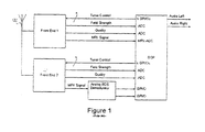
- FIG. 1 is a block diagram illustrating a prior art FM radio incorporating an analog RDS demodulator.
- FIG. 2 is a block diagram illustrating an FM radio incorporating a signal processing front-end for helping to recover data content in the FM radio signal without undue cost or complexity.
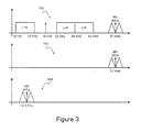
- FIG. 3 is a spectrum diagram that illustrates the effect of the front-end shown in Figure 2 on the received FM radio multiplex signal.
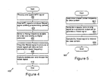
- FIG. 4 is a flow chart illustrating a method for processing an FM radio signal to make the data content recoverable without undue cost or complexity.
- FIG. 5 is a flow chart illustrating the steps taken by an FM signal processing system program run by the processor in the FM radio shown in FIG. 1.
- FIG. 2 illustrates an FM radio 200 that includes a reproduction front-end 202, a search front-end 204, and a processor 206.
- a filter 208 and a mixer 210 are connected to the search front-end 204 and where the processor 206 executes a program by calling from memory 212 an FM signal-processing program 214 capable of coordinating the reception on data content in an FM radio signal.
- memory 212 is depicted in Figure 2 as EEPROM onboard the processor 206, one skilled in the art will appreciate that a variety of memory storage areas may be used, including but not limited to, off-chip memory systems and their derivatives, or other types of on-chip memory storage devices including their derivatives.
- the front-ends 202, 204 generally act as receivers that include signal quality estimators as well as mixers and filters that separate out individual FM radio channels for processing by the processor 206.
- the processor 206 may be implemented as a general purpose microprocessor, digital signal processor (“DSP”), microcontroller, application specific integrated circuit (“ASIC”), reduced instruction set computer core (“RISC”), custom integrated circuit, Field Programmable Gate Array (“FPGA”), or their derivative successors.
- the processor 206 coordinates signal reception by the front-ends 202, 204 by employing the general-purpose input/output (“GPI/O") pins, and also includes one or more on-board analog-to-digital converters (“ADCs”) for digitizing analog input signals.
- GPI/O general-purpose input/output
- ADCs analog-to-digital converters
- the processor 206 may include one or more fast ADCs that support a sampling rate of 176.4 KHz, and one or more ADCs that support a sampling rate of 44.1 KHz.
- the ADCs may be delta-sigma ADCs that incorporate anti-aliasing filters.
- the processor 206 coordinates signal reception by outputting tuner control signals that cause the front-ends to tune to a selected frequency.
- the front-ends 202 and 204 extract the FM radio signal indicated by the processor 206, and provide field strength and quality indicators back to the processor 206.
- the processor may employ the indicators to determine when the reproduction receiver 202 should change frequency to begin reception of an FM channel with better signal quality.
- the search front-end 204 generally scans the FM spectrum in order to appraise the processor 206 of the signal quality available at different frequencies.
- the FM radio signal is generally a multiplexed FM radio signal ("MPX signal").
- the multiplexed signal includes both programming content and data content.
- the multiplexed signal may have the spectrum shown in Figure 3 as the MPX signal 302.
- left (L) and right (R) audio content may be present in the MPX signal.
- the programming content may include a summed L+R signal extending from 20 Hz to 15 KHz, a pilot tone at approximately 19 KHz, a lower sideband of an L-R signal extending from 23 KHz to 38 KHz, and an upper sideband of the L-R signal extending from 38 KHz to 53 KHz.
- the data content may include, as examples, an RDS or ARI signal centered on a 57 KHz subcarrier.
- programming content and data content are the information contained in two distinct spectral areas in a single FM radio channel.
- Information of any sort may be stored in the programming content and the data content.
- the programming content need not be audio information
- the data content need not be digital data.
- the search front-end 204 couples its MPX signal to the filter 208.
- the filter 208 may be, as an example, a high pass filter with a stop band below 33 KHz, a transition band between 33 and 55 KHz, and a pass band above 55 KHz.
- the filter 208 may be a bandpass filter with a passband between 55 and 59 KHz.
- the high pass filter may be implemented with a resistor-capacitor (RC) structure or other filter structure known in the art, while the bandpass filter may be implemented, for example, using a second order filter such as an active filter based on an operational amplifier, with a high Q value (e.g., approximately 10).
- RC resistor-capacitor
- the filters are not limited to the implementations noted above. Rather, many implementation variations of the filters are also suitable.
- the mixer 210 may be connected to the filtered output 212.
- the mixer 210 may be capable of shifting the frequency of the data content to a lower frequency than the original data content center frequency.
- the mixer 210 may shift the RDS data content from a center frequency of approximately 57 KHz to a center frequency of 12.9 KHz. This provides the resultant mixed signal on the frequency shifted signal output 214.
- the lower frequency may be selected according to the sampling rate(s) available to an ADC coupled to or on-board the processor 206. That is, the lower frequency may be chosen to spectrally place the data content at a bandwidth that a sampling rate available to a low-cost ADC allows the ADC to sample without significant aliasing or distortion.
- the mixer 210 may also be implemented as a chopper circuit - a multiplier that forms the product of the filtered signal on the filtered output 212 and a chopping signal (e.g., a square wave or other on / off) signal.
- the chopping signal frequency may be selected to shift the data content to a lower frequency that is suitable for digitization by an ADC coupled to or on-board the processor 206.
- the processor 206 selects the chopping signal frequency using the frequency control input 216. That is, the processor 206 generates the chopping signal on the frequency control input 216 by driving a general-purpose output pin between an a high (or signal-1) state and a low (or signal-0) state.
- the chopping signal frequency may be fixed and pre-selected, or provided by a dedicated signal source.
- the chopping signal frequency may be the same as the sampling frequency of the ADC that converts the mixed signal to digital form.
- the processor 206 may internally generate a sampling clock for the on-board ADC, and feed the sampling clock to the mixer 210 using a general purpose I/O pin.
- the ADC that converts the mixed signal may have a sampling rate of 44.1 KHz. As a result, the data content is shifted from 57 KHz down to 12.9 KHz.
- the ADC may be implemented as a delta-sigma ADC incorporating an anti-aliasing filter that removes any higher order mixing products.
- the MPX-ADC that converts the MPX signal from the reproduction front-end 202 may have a sampling rate of 176.4 KHz.
- Figure 2 illustrates the search receiver 204 coupled to the filter 208 and mixer 210
- a filter and mixer may instead be provided on the reproduction front-end 202, or both the reproduction front-end 202 and search front-end 204.
- Figure 3 shows spectrum diagrams 300 that illustrate the effect of the front-end system.
- Figure 3 shows the MPX signal 302 that includes both programming content (L and R audio information) and data content (RDS / ARI data).
- the filter 208 generates the filtered signal 304 on the filtered output 212. Note that the filtered output removes the programming content from the MPX signal.
- Figure 3 shows the mixed signal 306 that the mixer 210 generates on the frequency shifted signal output 214. Note that the mixed signal 306 still includes the data content, but that the data content is shifted to a lower center frequency of 12.9 KHz
- FIG. 4 summarizes a method for processing an FM radio signal to make the data content recoverable without undue cost or complexity.
- the FM radio 200 receives and outputs an MPX signal (402), for example, using the search front-end 204.
- the filter 208 filters the MPX signal to produce a filtered signal that eliminates the programming content present in the MPX signal (404). So that the FM radio may employ integrated low cost ADCs, a mixing frequency is selected for shifting the data content in the filtered signal to a lower frequency (406).
- the FM radio 200 then mixes the filtered signal to produce a mixed signal in which the data content is centered at the lower frequency (408).
- the processor 206 may then digitally demodulate, decode, output, and otherwise process the digital data present in the data content (410).
- FIG. 5 summarizes the steps taken by the FM signal-processing program 214 run by the processor 206 in the FM radio 200 shown in FIG. 2.
- the processing program 214 causes the processor 206 to determine a lower center frequency for the data content so that the data content may be digitized by an A-to-D converter in the processor 206 (502).
- the processor 206 may recall a parameter from memory or receive an input that indicates the lower center frequency.
- the parameter may be direct, for example setting forth the new center frequency explicitly, or indirect, for example setting forth the new center frequency in terms of another quantity, such as a mixing clock frequency to generate.
- the processing program 214 causes the processor 206 to generate a mixing signal according to the lower center frequency (504).
- the mixing signal is generally a square wave driven on a processor output pin to a chopping circuit.
- the chopping circuit mixes the FM radio signal to produce a mixed signal including the data content shifted to the lower center frequency.
- the processing program 214 then uses the A-to-D converter in the processor 206 to sample the mixed signal to recover the data content (506).
- the FM radio 200 no longer needs a separate dedicated analog RDS decoder. Rather, the FM radio 200 may eliminate the cost and complexity of the analog decoder, by replacing it with a lower complexity, relatively inexpensive circuitry.
- a front-end system formed from the search front-end 204, the filter 208, and mixer 210 provides the processor 206 with a frequency shifted data content signal that the processor 206 may digitize and process itself.
- the processing may include digital demodulation, decoding, error checking, message and data recovery, and the like, according to RDS or ARI signal specifications.
- the processor 206 may capture the data content using an ADC with a slower sampling rate (e.g., 44.1 KHz), resulting in cost and complexity savings over faster ADCs.
Landscapes
- Engineering & Computer Science (AREA)
- Computer Networks & Wireless Communication (AREA)
- Signal Processing (AREA)
- Circuits Of Receivers In General (AREA)
Priority Applications (2)
| Application Number | Priority Date | Filing Date | Title |
|---|---|---|---|
| EP04005164A EP1571757B1 (fr) | 2004-03-04 | 2004-03-04 | Processeur pour récepteurs radio FM |
| US11/071,017 US8229034B2 (en) | 2004-03-04 | 2005-03-03 | FM radio receiver processing system |
Applications Claiming Priority (1)
| Application Number | Priority Date | Filing Date | Title |
|---|---|---|---|
| EP04005164A EP1571757B1 (fr) | 2004-03-04 | 2004-03-04 | Processeur pour récepteurs radio FM |
Publications (2)
| Publication Number | Publication Date |
|---|---|
| EP1571757A1 true EP1571757A1 (fr) | 2005-09-07 |
| EP1571757B1 EP1571757B1 (fr) | 2012-05-23 |
Family
ID=34746003
Family Applications (1)
| Application Number | Title | Priority Date | Filing Date |
|---|---|---|---|
| EP04005164A Expired - Lifetime EP1571757B1 (fr) | 2004-03-04 | 2004-03-04 | Processeur pour récepteurs radio FM |
Country Status (2)
| Country | Link |
|---|---|
| US (1) | US8229034B2 (fr) |
| EP (1) | EP1571757B1 (fr) |
Families Citing this family (5)
| Publication number | Priority date | Publication date | Assignee | Title |
|---|---|---|---|---|
| US8059758B2 (en) * | 2006-02-10 | 2011-11-15 | Qualcomm, Incorporated | Conversion of multiple analog signals in an analog to digital converter |
| US8099072B2 (en) * | 2006-11-21 | 2012-01-17 | Qualcomm Incorporated | Frequency changer circuits |
| SG11201606303UA (en) * | 2014-02-04 | 2016-08-30 | Tactual Labs Co | Frequency conversion in a touch sensor |
| JP2017520201A (ja) * | 2014-04-25 | 2017-07-20 | ザ・リージェンツ・オブ・ザ・ユニバーシティ・オブ・ミシガンThe Regents Of The University Of Michigan | デジタル・ベースバンドが閾値付近である短距離ジグビー(zigbee(登録商標))互換受信機 |
| RU2759753C1 (ru) * | 2020-12-24 | 2021-11-17 | Владимир Григорьевич Бартенев | Способ измерения и индикации частоты для фм тюнера и устройство для его реализации |
Citations (5)
| Publication number | Priority date | Publication date | Assignee | Title |
|---|---|---|---|---|
| DE2200977A1 (de) | 1971-01-11 | 1972-07-20 | Du Pont | Trimerisierung von Butadien |
| EP0200977A2 (fr) * | 1985-05-07 | 1986-11-12 | Blaupunkt-Werke GmbH | Démodulateur numérique |
| US5459432A (en) * | 1993-07-22 | 1995-10-17 | Rockwell International Corporation | Use of a chopper and a sigma-delta modulator for downconverting and digitizing an analog signal including information modulated by a carrier |
| US6052569A (en) * | 1997-01-17 | 2000-04-18 | U.S. Philips Corporation | Radio receiver having a first tuner circuit for receiving signals in a first and a second frequency range, and a second tuner circuit for receiving signals in the first and a third frequency range |
| EP1241814A1 (fr) * | 2001-03-15 | 2002-09-18 | Siemens Aktiengesellschaft | Récepteur de Radiodiffusion RDS-TMC et Procédé de Calibration d'une Horloge Interne d'un Récepteur de Radiodiffusion |
Family Cites Families (13)
| Publication number | Priority date | Publication date | Assignee | Title |
|---|---|---|---|---|
| US4710956A (en) * | 1984-05-31 | 1987-12-01 | American Television & Communications Corporation | Cable television system |
| US4684980A (en) * | 1984-05-31 | 1987-08-04 | American Television & Communications Corporation | System for controlling communications on a cable television network |
| US4816769A (en) * | 1985-06-21 | 1989-03-28 | Ma John Y | BPSK demodulator and FM receiver for digital data pagers |
| US5257312A (en) * | 1991-05-03 | 1993-10-26 | U.S. Philips Corporation | Time-discrete stereo decoder |
| DE4309518A1 (de) * | 1993-03-24 | 1994-10-06 | Blaupunkt Werke Gmbh | Schaltungsanordnung zur Ableitung mindestens eines von der Qualität eines empfangenen Signals abhängigen Qualitätssignals |
| US5517529A (en) * | 1993-10-18 | 1996-05-14 | Westinghouse Electric Corp. | UHF/L-Band monolithic direct digital receiver |
| US5448299A (en) * | 1994-01-05 | 1995-09-05 | Samsung Electronics Co., Ltd. | Apparatus for processing BPSK signals transmitted with NTSC TV on quadrature-phase video carrier |
| US5636252A (en) * | 1994-05-04 | 1997-06-03 | Samsung Electronics Co., Ltd. | Automatic gain control of radio receiver for receiving digital high-definition television signals |
| US5479449A (en) * | 1994-05-04 | 1995-12-26 | Samsung Electronics Co. Ltd. | Digital VSB detector with bandpass phase tracker, as for inclusion in an HDTV receiver. |
| JP2966785B2 (ja) * | 1995-12-21 | 1999-10-25 | 全国朝日放送株式会社 | 多重放送受信装置 |
| EP1432157B1 (fr) * | 2002-12-20 | 2007-09-19 | Sony Deutschland GmbH | Procédé d'extraction d'une composante de signal RDS et récepteur de signaux |
| US7542505B2 (en) * | 2003-10-20 | 2009-06-02 | Northrop Grumman Corporation | Systems and methods for signal conversion |
| US20050144648A1 (en) * | 2003-10-31 | 2005-06-30 | Gotwals Michael D. | Communication network analysis apparatus with internetwork connectivity |
-
2004
- 2004-03-04 EP EP04005164A patent/EP1571757B1/fr not_active Expired - Lifetime
-
2005
- 2005-03-03 US US11/071,017 patent/US8229034B2/en active Active
Patent Citations (5)
| Publication number | Priority date | Publication date | Assignee | Title |
|---|---|---|---|---|
| DE2200977A1 (de) | 1971-01-11 | 1972-07-20 | Du Pont | Trimerisierung von Butadien |
| EP0200977A2 (fr) * | 1985-05-07 | 1986-11-12 | Blaupunkt-Werke GmbH | Démodulateur numérique |
| US5459432A (en) * | 1993-07-22 | 1995-10-17 | Rockwell International Corporation | Use of a chopper and a sigma-delta modulator for downconverting and digitizing an analog signal including information modulated by a carrier |
| US6052569A (en) * | 1997-01-17 | 2000-04-18 | U.S. Philips Corporation | Radio receiver having a first tuner circuit for receiving signals in a first and a second frequency range, and a second tuner circuit for receiving signals in the first and a third frequency range |
| EP1241814A1 (fr) * | 2001-03-15 | 2002-09-18 | Siemens Aktiengesellschaft | Récepteur de Radiodiffusion RDS-TMC et Procédé de Calibration d'une Horloge Interne d'un Récepteur de Radiodiffusion |
Also Published As
| Publication number | Publication date |
|---|---|
| US20050195920A1 (en) | 2005-09-08 |
| US8229034B2 (en) | 2012-07-24 |
| EP1571757B1 (fr) | 2012-05-23 |
Similar Documents
| Publication | Publication Date | Title |
|---|---|---|
| US6373422B1 (en) | Method and apparatus employing decimation filter for down conversion in a receiver | |
| US6256358B1 (en) | Digital signal processing architecture for multi-band radio receiver | |
| EP0716518A2 (fr) | Démodulateur quadrature à bande étroite pour radiodiffusion numérique par satellite | |
| US8229034B2 (en) | FM radio receiver processing system | |
| US6052569A (en) | Radio receiver having a first tuner circuit for receiving signals in a first and a second frequency range, and a second tuner circuit for receiving signals in the first and a third frequency range | |
| US6714600B1 (en) | Receiver | |
| US20070021081A1 (en) | Receiver unit and method for receiving an analogue received signal | |
| AU747696B2 (en) | Direct frequency selection and down-conversion for digital receivers | |
| US20120140859A1 (en) | Method and control unit for direct sampling of a plurality of radio bands | |
| US8111786B2 (en) | Signal converters | |
| US8644429B2 (en) | Digital downconversion and fast channel selection of narrowband signals using a wide band RF tuner | |
| KR950016386A (ko) | 아날로그/디지탈 위성방송 겸용수신기 | |
| EP1177635A1 (fr) | Circuit recepteur | |
| US20060189291A1 (en) | Receiver and method for concurrent receiving of multiple channels | |
| US8099071B2 (en) | Direct conversion pre-ADC frequency mixer | |
| JP4903633B2 (ja) | 道路交通情報通信システム用チューナ | |
| JP2001094450A5 (ja) | 受信機およびそのic | |
| KR100671299B1 (ko) | 텔레비전 장치 및 텔레비전 장치의 제어방법 | |
| KR20020069754A (ko) | 아날로그 및 디지털 방송 복합 수신기 | |
| JPH0583707A (ja) | Cs音声放送受信機の表示装置 | |
| JP2002016513A (ja) | 受信回路 | |
| KR200421705Y1 (ko) | Dmb 안테나 모듈 | |
| CN101339034A (zh) | 接收数字广播信号和导航定位信号的电路系统和方法 | |
| KR100872547B1 (ko) | 비에스 튜너와 지피에스 수신기가 일체화된 튜너 및 이를 구비하는 네비게이션 시스템 | |
| JP2006522564A (ja) | マルチ・チャンネル衛星放送信号の受信装置 |
Legal Events
| Date | Code | Title | Description |
|---|---|---|---|
| PUAI | Public reference made under article 153(3) epc to a published international application that has entered the european phase |
Free format text: ORIGINAL CODE: 0009012 |
|
| AK | Designated contracting states |
Kind code of ref document: A1 Designated state(s): AT BE BG CH CY CZ DE DK EE ES FI FR GB GR HU IE IT LI LU MC NL PL PT RO SE SI SK TR |
|
| AX | Request for extension of the european patent |
Extension state: AL LT LV MK |
|
| 17P | Request for examination filed |
Effective date: 20060307 |
|
| AKX | Designation fees paid |
Designated state(s): AT BE BG CH CY CZ DE DK EE ES FI FR GB GR HU IE IT LI LU MC NL PL PT RO SE SI SK TR |
|
| RAP1 | Party data changed (applicant data changed or rights of an application transferred) |
Owner name: HARMAN BECKER AUTOMOTIVE SYSTEMS GMBH |
|
| 17Q | First examination report despatched |
Effective date: 20070927 |
|
| GRAP | Despatch of communication of intention to grant a patent |
Free format text: ORIGINAL CODE: EPIDOSNIGR1 |
|
| GRAS | Grant fee paid |
Free format text: ORIGINAL CODE: EPIDOSNIGR3 |
|
| GRAA | (expected) grant |
Free format text: ORIGINAL CODE: 0009210 |
|
| AK | Designated contracting states |
Kind code of ref document: B1 Designated state(s): AT BE BG CH CY CZ DE DK EE ES FI FR GB GR HU IE IT LI LU MC NL PL PT RO SE SI SK TR |
|
| REG | Reference to a national code |
Ref country code: GB Ref legal event code: FG4D |
|
| REG | Reference to a national code |
Ref country code: CH Ref legal event code: EP |
|
| REG | Reference to a national code |
Ref country code: AT Ref legal event code: REF Ref document number: 559484 Country of ref document: AT Kind code of ref document: T Effective date: 20120615 |
|
| REG | Reference to a national code |
Ref country code: IE Ref legal event code: FG4D |
|
| REG | Reference to a national code |
Ref country code: DE Ref legal event code: R096 Ref document number: 602004037866 Country of ref document: DE Effective date: 20120719 |
|
| REG | Reference to a national code |
Ref country code: NL Ref legal event code: VDEP Effective date: 20120523 |
|
| PG25 | Lapsed in a contracting state [announced via postgrant information from national office to epo] |
Ref country code: SE Free format text: LAPSE BECAUSE OF FAILURE TO SUBMIT A TRANSLATION OF THE DESCRIPTION OR TO PAY THE FEE WITHIN THE PRESCRIBED TIME-LIMIT Effective date: 20120523 Ref country code: FI Free format text: LAPSE BECAUSE OF FAILURE TO SUBMIT A TRANSLATION OF THE DESCRIPTION OR TO PAY THE FEE WITHIN THE PRESCRIBED TIME-LIMIT Effective date: 20120523 Ref country code: CY Free format text: LAPSE BECAUSE OF FAILURE TO SUBMIT A TRANSLATION OF THE DESCRIPTION OR TO PAY THE FEE WITHIN THE PRESCRIBED TIME-LIMIT Effective date: 20120523 |
|
| REG | Reference to a national code |
Ref country code: AT Ref legal event code: MK05 Ref document number: 559484 Country of ref document: AT Kind code of ref document: T Effective date: 20120523 |
|
| PG25 | Lapsed in a contracting state [announced via postgrant information from national office to epo] |
Ref country code: GR Free format text: LAPSE BECAUSE OF FAILURE TO SUBMIT A TRANSLATION OF THE DESCRIPTION OR TO PAY THE FEE WITHIN THE PRESCRIBED TIME-LIMIT Effective date: 20120824 Ref country code: SI Free format text: LAPSE BECAUSE OF FAILURE TO SUBMIT A TRANSLATION OF THE DESCRIPTION OR TO PAY THE FEE WITHIN THE PRESCRIBED TIME-LIMIT Effective date: 20120523 Ref country code: PT Free format text: LAPSE BECAUSE OF FAILURE TO SUBMIT A TRANSLATION OF THE DESCRIPTION OR TO PAY THE FEE WITHIN THE PRESCRIBED TIME-LIMIT Effective date: 20120924 |
|
| PG25 | Lapsed in a contracting state [announced via postgrant information from national office to epo] |
Ref country code: BE Free format text: LAPSE BECAUSE OF FAILURE TO SUBMIT A TRANSLATION OF THE DESCRIPTION OR TO PAY THE FEE WITHIN THE PRESCRIBED TIME-LIMIT Effective date: 20120523 |
|
| PG25 | Lapsed in a contracting state [announced via postgrant information from national office to epo] |
Ref country code: SK Free format text: LAPSE BECAUSE OF FAILURE TO SUBMIT A TRANSLATION OF THE DESCRIPTION OR TO PAY THE FEE WITHIN THE PRESCRIBED TIME-LIMIT Effective date: 20120523 Ref country code: RO Free format text: LAPSE BECAUSE OF FAILURE TO SUBMIT A TRANSLATION OF THE DESCRIPTION OR TO PAY THE FEE WITHIN THE PRESCRIBED TIME-LIMIT Effective date: 20120523 Ref country code: EE Free format text: LAPSE BECAUSE OF FAILURE TO SUBMIT A TRANSLATION OF THE DESCRIPTION OR TO PAY THE FEE WITHIN THE PRESCRIBED TIME-LIMIT Effective date: 20120523 Ref country code: CZ Free format text: LAPSE BECAUSE OF FAILURE TO SUBMIT A TRANSLATION OF THE DESCRIPTION OR TO PAY THE FEE WITHIN THE PRESCRIBED TIME-LIMIT Effective date: 20120523 Ref country code: NL Free format text: LAPSE BECAUSE OF FAILURE TO SUBMIT A TRANSLATION OF THE DESCRIPTION OR TO PAY THE FEE WITHIN THE PRESCRIBED TIME-LIMIT Effective date: 20120523 Ref country code: DK Free format text: LAPSE BECAUSE OF FAILURE TO SUBMIT A TRANSLATION OF THE DESCRIPTION OR TO PAY THE FEE WITHIN THE PRESCRIBED TIME-LIMIT Effective date: 20120523 Ref country code: AT Free format text: LAPSE BECAUSE OF FAILURE TO SUBMIT A TRANSLATION OF THE DESCRIPTION OR TO PAY THE FEE WITHIN THE PRESCRIBED TIME-LIMIT Effective date: 20120523 |
|
| PG25 | Lapsed in a contracting state [announced via postgrant information from national office to epo] |
Ref country code: IT Free format text: LAPSE BECAUSE OF FAILURE TO SUBMIT A TRANSLATION OF THE DESCRIPTION OR TO PAY THE FEE WITHIN THE PRESCRIBED TIME-LIMIT Effective date: 20120523 Ref country code: PL Free format text: LAPSE BECAUSE OF FAILURE TO SUBMIT A TRANSLATION OF THE DESCRIPTION OR TO PAY THE FEE WITHIN THE PRESCRIBED TIME-LIMIT Effective date: 20120523 |
|
| PLBE | No opposition filed within time limit |
Free format text: ORIGINAL CODE: 0009261 |
|
| STAA | Information on the status of an ep patent application or granted ep patent |
Free format text: STATUS: NO OPPOSITION FILED WITHIN TIME LIMIT |
|
| PG25 | Lapsed in a contracting state [announced via postgrant information from national office to epo] |
Ref country code: ES Free format text: LAPSE BECAUSE OF FAILURE TO SUBMIT A TRANSLATION OF THE DESCRIPTION OR TO PAY THE FEE WITHIN THE PRESCRIBED TIME-LIMIT Effective date: 20120903 |
|
| 26N | No opposition filed |
Effective date: 20130226 |
|
| REG | Reference to a national code |
Ref country code: DE Ref legal event code: R097 Ref document number: 602004037866 Country of ref document: DE Effective date: 20130226 |
|
| PG25 | Lapsed in a contracting state [announced via postgrant information from national office to epo] |
Ref country code: BG Free format text: LAPSE BECAUSE OF FAILURE TO SUBMIT A TRANSLATION OF THE DESCRIPTION OR TO PAY THE FEE WITHIN THE PRESCRIBED TIME-LIMIT Effective date: 20120823 |
|
| PG25 | Lapsed in a contracting state [announced via postgrant information from national office to epo] |
Ref country code: MC Free format text: LAPSE BECAUSE OF NON-PAYMENT OF DUE FEES Effective date: 20130331 |
|
| REG | Reference to a national code |
Ref country code: CH Ref legal event code: PL |
|
| REG | Reference to a national code |
Ref country code: IE Ref legal event code: MM4A |
|
| PG25 | Lapsed in a contracting state [announced via postgrant information from national office to epo] |
Ref country code: IE Free format text: LAPSE BECAUSE OF NON-PAYMENT OF DUE FEES Effective date: 20130304 Ref country code: LI Free format text: LAPSE BECAUSE OF NON-PAYMENT OF DUE FEES Effective date: 20130331 Ref country code: CH Free format text: LAPSE BECAUSE OF NON-PAYMENT OF DUE FEES Effective date: 20130331 |
|
| PG25 | Lapsed in a contracting state [announced via postgrant information from national office to epo] |
Ref country code: TR Free format text: LAPSE BECAUSE OF FAILURE TO SUBMIT A TRANSLATION OF THE DESCRIPTION OR TO PAY THE FEE WITHIN THE PRESCRIBED TIME-LIMIT Effective date: 20120523 |
|
| PG25 | Lapsed in a contracting state [announced via postgrant information from national office to epo] |
Ref country code: HU Free format text: LAPSE BECAUSE OF FAILURE TO SUBMIT A TRANSLATION OF THE DESCRIPTION OR TO PAY THE FEE WITHIN THE PRESCRIBED TIME-LIMIT; INVALID AB INITIO Effective date: 20040304 Ref country code: LU Free format text: LAPSE BECAUSE OF NON-PAYMENT OF DUE FEES Effective date: 20130304 |
|
| REG | Reference to a national code |
Ref country code: FR Ref legal event code: PLFP Year of fee payment: 13 |
|
| REG | Reference to a national code |
Ref country code: FR Ref legal event code: PLFP Year of fee payment: 14 |
|
| REG | Reference to a national code |
Ref country code: FR Ref legal event code: PLFP Year of fee payment: 15 |
|
| PGFP | Annual fee paid to national office [announced via postgrant information from national office to epo] |
Ref country code: FR Payment date: 20230222 Year of fee payment: 20 |
|
| PGFP | Annual fee paid to national office [announced via postgrant information from national office to epo] |
Ref country code: GB Payment date: 20230223 Year of fee payment: 20 Ref country code: DE Payment date: 20230221 Year of fee payment: 20 |
|
| P01 | Opt-out of the competence of the unified patent court (upc) registered |
Effective date: 20230526 |
|
| REG | Reference to a national code |
Ref country code: DE Ref legal event code: R071 Ref document number: 602004037866 Country of ref document: DE |
|
| REG | Reference to a national code |
Ref country code: GB Ref legal event code: PE20 Expiry date: 20240303 |
|
| PG25 | Lapsed in a contracting state [announced via postgrant information from national office to epo] |
Ref country code: GB Free format text: LAPSE BECAUSE OF EXPIRATION OF PROTECTION Effective date: 20240303 |