EP1575001A2 - Dispositif pour identifier des feuilles - Google Patents
Dispositif pour identifier des feuilles Download PDFInfo
- Publication number
- EP1575001A2 EP1575001A2 EP04019825A EP04019825A EP1575001A2 EP 1575001 A2 EP1575001 A2 EP 1575001A2 EP 04019825 A EP04019825 A EP 04019825A EP 04019825 A EP04019825 A EP 04019825A EP 1575001 A2 EP1575001 A2 EP 1575001A2
- Authority
- EP
- European Patent Office
- Prior art keywords
- identification
- paper sheet
- unit
- characteristics information
- image data
- Prior art date
- Legal status (The legal status is an assumption and is not a legal conclusion. Google has not performed a legal analysis and makes no representation as to the accuracy of the status listed.)
- Withdrawn
Links
Images


Classifications
-
- G—PHYSICS
- G07—CHECKING-DEVICES
- G07D—HANDLING OF COINS OR VALUABLE PAPERS, e.g. TESTING, SORTING BY DENOMINATIONS, COUNTING, DISPENSING, CHANGING OR DEPOSITING
- G07D7/00—Testing specially adapted to determine the identity or genuineness of valuable papers or for segregating those which are unacceptable, e.g. banknotes that are alien to a currency
- G07D7/06—Testing specially adapted to determine the identity or genuineness of valuable papers or for segregating those which are unacceptable, e.g. banknotes that are alien to a currency using wave or particle radiation
- G07D7/12—Visible light, infrared or ultraviolet radiation
Definitions
- the present invention relates to a paper sheet identifier device for valuable stocks and bonds, and paper notes.
- the present invention has been made in view of the above circumstances and has an object to overcome the above problems and to provide a paper sheet identifier device, which allows a high speed processing in the identification of paper sheets including stocks and bonds as well as paper currencies, in addition to rapid accommodation to newly issued paper sheets.
- the present invention provides a paper sheet identifier device including: a sensor for detecting any necessary characteristics of a paper sheet required for identifying the paper sheet; a characteristics information collector unit for converting the output signal from the sensor to the characteristics information of the paper sheet; an identifying unit for identifying the paper sheet by using the characteristics information output from the characteristics information collector unit; and a controller unit for controlling the characteristics information collector unit and the identifying unit, in which the controller unit adjusts the number of connections to the identifying unit and the characteristics information collector unit, depending on the type of paper sheets or the speed of identifying process.
- the present invention provides a paper sheet identifier device embodying the improvement of identification speed by virtue of the parallel implementation of identification processes, along with the improvement of efficiency when changing the specification of paper sheet identifier device in correspondence with the new currency notes issued.
- the type and denomination of notes and the identification method of authentic notes differs for every country.
- the preferred embodiment of the present invention accordingly provides a main board for performing common processes of currency notes that is independent of country specific method (i.e., identification preprocessing and final determination), and auxiliary boards operated in parallel (for identification and sensor control).
- the hardware configuration can be altered to suit the note identification requirement of each country by simply adding or replacing the auxiliary boards connected to the main board.
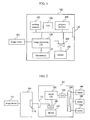
- FIG. 1 there is shown a schematic circuit diagram of the main board used in the identification device in accordance with one preferred embodiment of the present invention.
- An image sensor 101 is a means for outputting sequentially image signal of cross feed lines of a currency note, which means can be implemented by a CCD image sensor having a plurality of semiconductor photoelectric transducer elements placed inline.
- a main board 102 is an electronics board for mounting elements for performing the identification process of currency notes.
- a program memory 105 is a memory for storing the program used for the identification process, and can be implemented by the semiconductor memory.
- An image processing LSI 106 is a means for converting the image signal of currency note scanned by the image sensor 101 into the image data suitable for the identification process, which LSI can be implemented by a semiconductor integrated circuit.
- a line memory 107 is a means for storing image data of several scan lines of cross feed direction used by the image processing LSI 106 for the image processing, which memory can be implemented by the semiconductor memory.
- a switch 108 is a switching means for switching the access to an SRAM 109 from either the CPU 104 or the image processing LSI 106, which switch can be implemented by a semiconductor analog switch.
- the SRAM 109 is a temporary storage means of the result of image processing of the surface of notes processed by the image processing LSI 106, which SRAM can be implemented by a semiconductor memory.
- a connector 110 is a means for connecting a system bus to other boards. The connector 110 will be described in greater details later.
- the operation of the main board 102 will be described with reference to Fig. 1.
- the surface image of a currency note is imaged by the image sensor 101 to obtain image signal for each line of cross feed direction.
- the image processing LSI 106 temporarily stores the image data for the scan line into the line memory 107 and performing the image processing by reading out a plurality of lines of image data.
- a typical image processing includes filter operation such as smoothing and edge enhancement, and gradation conversion such as binarization.
- the image processing results from the image processing LSI 106 is stored in the SRAM 109 through the switch 108, one scan line at a time.
- the image processing LSI 106 issues to the CPU 104 an image processing termination interrupt signal.
- the CPU 104 upon reception of the interrupt signal reads out the image processing results from the SRAM 109 through the switch 108, to transfer the image to the working memory 103.
- the CPU 104 performs data generation for identification until the image processing termination interrupt signal for the next scan line is issued from the image processing LSI 106.
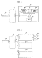
- FIG. 2 there is shown a schematic diagram of a sensor board 201 connected to the main board 102.
- Sensors 208, 209, 210 are provided for detecting characteristics of a note.
- the characteristics of a currency note include for example the watermark, hologram, fluorescent ink and the like, in order to prevent counterfeit.
- the sensors 208, 209, 210 detect these characteristics.
- An analog switch 204 is a switching means for sequentially switching the analog signal input from the sensors 208, 209, 210 to an A/D Converter 203, which switch can be implemented by a semiconductor analog switch.
- the A/D Converter 203 is a means for converting the analog signal from the sensors 208, 209, 21 0 into the digital signal, which converter can be implemented by a semiconductor A/D converter.
- a sensor LSI 202 controls the operation of the sensors 208, 209, and 210, performs digital operation such as averaging between two adjacent data units on the data of the sensors 208, 209, 210 input through the A/D Converter 203, and outputs to an SRAM 206, which LSI can be implemented by a semiconductor logic LSI.
- An analog switch 205 is a means for switching the access to the SRAM 206 from either the CPU 104 of the main board or the sensor LSI 202, which switch can be implemented by a semiconductor analog switch.
- the SRAM 206 is a means for storing the sensor data for just one sheet of currency note from the sensor LSI 202, which SRAM can be implemented by a semiconductor memory capable of reading and writing data.
- the A/D converter 203 converts the analog signal into the digital signal to feed to the sensor LSI 202, which performs the digital operation thereon separately for the sensor output.
- the analog switch 205 connects the SRAM 206 to the sensor LSI 202 to store the data processed by the sensor LSI 202 into addresses in the SRAM 206 specified for the data.
- the main board 102 and the sensor board 201 are separately configured. However, these two boards can be integrated into one single board.
- FIG. 3 there is shown a schematic diagram of an identification board 301 connected to the main board 102.
- a working memory 302 is a memory for data storage for a CPU 303 to perform an identification processing, which memory can be implemented by a semiconductor memory.
- the CPU 303 performs the identification processing.
- a program memory 304 is a memory for storing the identification processing program, which memory can be implemented by a semiconductor memory.
- a switch 305 is a switching means for switching the access to an SRAM 306 from either the CPU 104 on the main board 102 or the CPU 303 on the identification board 301, which switch can be implemented by a semiconductor analog switch.
- the SRAM 306 is a memory for storing the note data for identification transferred from the CPU 104 on the main board 102, which SRAM can be implemented by a semiconductor memory.
- the operation of the identification board 301 will be described with reference to Fig. 3.
- the switch 305 switches the connection to the CPU 303.
- the CPU 303 reads the data for identification from the SRAM 306 to store it in the working memory 302. This operation for one scan line is iteratively repeated for one currency note before the CPU 303 performs the identification processing.
- the identification result information obtained by the identification processing will be stored in the specified address in the SRAM 306.
- the identification result information to be stored includes for example the denomination of the note, and the result of determination of authenticity.
- the main board 102 and the identification board 301 are separately configured. However, these two boards can be integrated into one single board.
- Fig. 4 there is shown a schematic diagram of a paper sheet identifier device having the main board 102 connected to the sensor board 201, identification board 301a and identification board 301b.
- the identification boards 301a, 301b are configured identical to the identification board 301 described with reference to Fig. 3, and the circuit on those boards will be described using the same reference numbers described in Fig. 3.
- FIG. 5 there is shown a perspective view of the paper sheet identifier device shown in Fig. 4.
- the interface signal for connecting the main board 102 with the sensor board 201, and the identification boards 301a, 301b is common in every board, so that boards can be stacked as shown in Fig. 5 by means of a plurality of connectors 110 of the same specification.
- the order of stacking the identification boards 301a, 301b and the sensor board 201 can be arbitrary with respect to the main board 102.
- the identification boards 301a, 301b can be swapped.
- the main board 102, the sensor board 201, and the identification board 301 are separately configured.
- these two boards can be integrated into one single board, with the type and number of mounted elements altered.
- the address signal A0 to An, data signal D0 to Dm, read signal RDN, write signal WRN are signals for reading and writing data for the addresses on the SRAM 206 and the SRAM 306 on the sensor board and identification board.
- the bus switch signals BS1 to BSp are signals for switching the switches 205 and 305 on the sensor board 201 and the identification board 301, respectively.
- the interrupt signal IRO to IRp are signals for connecting interrupt signals from the sensor LSI 202 on the sensor board to the CPU 104 on the main board, and interrupt signals from the image processing LSI 106 on the main board to the CPU 303 on the identification board.
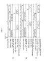
- FIG. 7 The operation timing chart for one scan line of cross feed direction in the paper sheet identifier device shown in Fig. 4 is shown in Fig. 7.
- the operation timing chart of the main board 102 is shown in Fig. 7 (a).
- the image sensor 101 captures image data for one scan line of cross feed direction to obtain the surface image of a currency note, the operation of image sensor 101 is controlled by the line synchronization signal output from the image processing LSI 106.
- the image processing LSI 106 retrieves the image data of one preceding scan line from the line memory 107 to perform image processing, and stores the image processing result for one scan line into the SRAM 109 through the switch 108.
- the image processing LSI 106 issues an interrupt signal for notifying the CPU 104 of the completion of image processing.
- the CPU 104 upon reception of the interrupt, will read out the image processing result from the SRAM 109 through the switch 108 to transfer the image to the working memory 103.
- the operation timing chart of the sensor board 201 is shown in Fig. 7 (b).
- Each of the sensors 208, 209, and 210 captures the characteristics for one scan line of main scan direction for determining the authenticity of a currency note, in accordance with the line synchronization signal output from the image processing LSI 106.
- the sensor LSI 202 operates on the sensor data of just one preceding scan line to store the result into the SRAM 206 through the analog switch 205 for each scan line.
- the sensor LSI 202 issues an interrupt to the CPU 104 on the main board 102 for notifying the CPU 104 of the completion of sensor operation.
- the CPU 104 upon reception of the interrupt, will read the operation results from the SRAM 206 through the analog switch 205 to transfer data to the working memory 103 on the main board 102.
- the identification boards 301a, 301b will be described.
- the operation timing chart is shown in Fig. 7 (c).
- the CPU 104 transfers the data for identification from the working memory 103 to the SRAM 306 on the identification boards 301a, 301b.
- the CPU 303 on the identification boards 301a, 301b will transfer the data for identification stored in the SRAM 306 into the working memory 302, during the time when the CPU 104 on the main board 102 transfers the image data from the SRAM 109 to the working memory 103.
- the CPU 104 on the main board 102 generates the identification data required for the determination of denomination and authenticity of the input note, based on the image data output from the image processing LSI 106 along with the sensor data output from the sensor LSI 202, and stores the data to the SRAM 306 on the identification boards 301a, 301b.
- the CPUs 303 on the identification boards 301a, 301b perform the determination processing of denomination in parallel processing.
- the identification programs stored in the program memory 304 on the identification boards 301a, 301b can identify different denominations, for example the CPU 303 on the identification board 301a may recognize the denomination and then authenticity of the notes in current circulation, while on the other hand the CPU 303 on the identification board 301b may recognize the denomination and then authenticity of the notes newly issued, in parallel.
- the determination results from those CPUs are notified to the CPU 104 on the main board 102 simultaneously.
- the notification process may be such that each CPU on the identification board independently writes the determination result in the address specified of the SRAM 306, and thereafter the CPU 104 on the main board 102 reads the data of the specified addresses of the memory on the identification boards. Thereafter the CPU 104 on the main board 102 will perform the final determination based on the determination results from the identification boards 301a, 301b to terminate the determination for one currency note.
- the paper sheet identifier device in accordance with the present invention may have the effect that it can add an additional identification board without updating the program or replacement of identification boards, when a new note is issued which contains a more complex scheme for authenticity identification, resulting in an improved efficiency of circulation of new notes.
- the paper sheet identifier device of the present invention may also have the effect that, since the main board 102 performs the common processing independent from the type and denomination of notes, while the different identification processes dependent on the notes can be executed in parallel, it allows the identification time to be saved, and the processing time can be maintained by adding more identification boards if there are many types and denomination of notes.
- the transfer time can be shorten to the time required for the effective data when the CPU on the main board stores the output data from the image processing LSI into the memory while the image data and image processing result required for the identification are written into the memory of identification boards in parallel.
- each of CPUs is allowed performing identification processing in parallel and independently.
Landscapes
- Health & Medical Sciences (AREA)
- General Health & Medical Sciences (AREA)
- Toxicology (AREA)
- Physics & Mathematics (AREA)
- General Physics & Mathematics (AREA)
- Inspection Of Paper Currency And Valuable Securities (AREA)
- Image Processing (AREA)
Applications Claiming Priority (2)
| Application Number | Priority Date | Filing Date | Title |
|---|---|---|---|
| JP2004068304 | 2004-03-11 | ||
| JP2004068304A JP4422515B2 (ja) | 2004-03-11 | 2004-03-11 | 紙葉類鑑別装置 |
Publications (2)
| Publication Number | Publication Date |
|---|---|
| EP1575001A2 true EP1575001A2 (fr) | 2005-09-14 |
| EP1575001A3 EP1575001A3 (fr) | 2005-11-23 |
Family
ID=34824594
Family Applications (1)
| Application Number | Title | Priority Date | Filing Date |
|---|---|---|---|
| EP04019825A Withdrawn EP1575001A3 (fr) | 2004-03-11 | 2004-08-20 | Dispositif pour identifier des feuilles |
Country Status (4)
| Country | Link |
|---|---|
| US (1) | US7621440B2 (fr) |
| EP (1) | EP1575001A3 (fr) |
| JP (1) | JP4422515B2 (fr) |
| CN (1) | CN100557622C (fr) |
Cited By (2)
| Publication number | Priority date | Publication date | Assignee | Title |
|---|---|---|---|---|
| EP2482256A4 (fr) * | 2009-09-24 | 2013-04-24 | Glory Kogyo Kk | Dispositif d'identification de feuilles de papier et procédé d'identification de feuilles de papier |
| WO2014090405A1 (fr) * | 2012-12-13 | 2014-06-19 | Giesecke & Devrient Gmbh | Système et procédé d'évaluation d'un flux de données de capteurs pour des documents de valeur |
Families Citing this family (10)
| Publication number | Priority date | Publication date | Assignee | Title |
|---|---|---|---|---|
| JP4977528B2 (ja) * | 2007-05-29 | 2012-07-18 | 株式会社サキコーポレーション | 外観検査装置およびシステム |
| CN101796550B (zh) * | 2007-09-07 | 2012-12-12 | 光荣株式会社 | 纸张类识别装置和纸张类识别方法 |
| US8194146B2 (en) * | 2008-01-11 | 2012-06-05 | Mediatek Inc. | Apparatuses for capturing and storing real-time images |
| US8682056B2 (en) * | 2008-06-30 | 2014-03-25 | Ncr Corporation | Media identification |
| JP5263513B2 (ja) * | 2008-09-30 | 2013-08-14 | 日本電産コパル株式会社 | 硬貨識別装置 |
| WO2012042571A1 (fr) * | 2010-09-29 | 2012-04-05 | グローリー株式会社 | Dispositif et procédé d'identification de feuilles de papier |
| KR101164566B1 (ko) | 2011-07-04 | 2012-07-13 | 기산전자 주식회사 | 자동으로 다국가 권종을 식별하는 지폐계수방법 |
| CN102831694B (zh) * | 2012-08-09 | 2015-01-14 | 广州广电运通金融电子股份有限公司 | 一种图像识别系统及图像存储控制方法 |
| JP6246625B2 (ja) * | 2014-03-11 | 2017-12-13 | 株式会社東芝 | 紙葉類処理装置およびデータ転送方法 |
| DE102016002897A1 (de) * | 2015-04-28 | 2016-11-03 | Giesecke & Devrient Gmbh | Wertdokumentbearbeitungsvorrichtung mit einem Datenkommunikationssystem und Verfahren zur Verteilung von Sensordaten in einer Wertdokumentbearbeitungsvorrichtung |
Citations (1)
| Publication number | Priority date | Publication date | Assignee | Title |
|---|---|---|---|---|
| US4091271A (en) | 1974-01-10 | 1978-05-23 | Umc Industries, Inc. | Validator for scrip |
Family Cites Families (8)
| Publication number | Priority date | Publication date | Assignee | Title |
|---|---|---|---|---|
| GB1385181A (en) | 1971-02-02 | 1975-02-26 | Europa Systems Ltd | Currency note acceptor |
| US5416307A (en) | 1993-09-03 | 1995-05-16 | Danek; Robert | Currency paper verification and denomination device |
| GB2309299B (en) * | 1996-01-16 | 2000-06-07 | Mars Inc | Sensing device |
| US6573983B1 (en) * | 1996-11-15 | 2003-06-03 | Diebold, Incorporated | Apparatus and method for processing bank notes and other documents in an automated banking machine |
| US5923413A (en) * | 1996-11-15 | 1999-07-13 | Interbold | Universal bank note denominator and validator |
| EP0901282B1 (fr) * | 1997-09-03 | 2006-06-28 | Hitachi, Ltd. | Procédé pour enregistrer et reproduire de l'information de filigrane électronique |
| US7054463B2 (en) * | 1998-01-20 | 2006-05-30 | Digimarc Corporation | Data encoding using frail watermarks |
| EP1361547A3 (fr) | 1998-01-23 | 2005-03-30 | BEB Industrie-Elektronik AG | Capteur de position |
-
2004
- 2004-03-11 JP JP2004068304A patent/JP4422515B2/ja not_active Expired - Fee Related
- 2004-07-09 CN CNB2004100697290A patent/CN100557622C/zh not_active Expired - Fee Related
- 2004-08-19 US US10/921,334 patent/US7621440B2/en not_active Expired - Fee Related
- 2004-08-20 EP EP04019825A patent/EP1575001A3/fr not_active Withdrawn
Patent Citations (1)
| Publication number | Priority date | Publication date | Assignee | Title |
|---|---|---|---|---|
| US4091271A (en) | 1974-01-10 | 1978-05-23 | Umc Industries, Inc. | Validator for scrip |
Cited By (4)
| Publication number | Priority date | Publication date | Assignee | Title |
|---|---|---|---|---|
| EP2482256A4 (fr) * | 2009-09-24 | 2013-04-24 | Glory Kogyo Kk | Dispositif d'identification de feuilles de papier et procédé d'identification de feuilles de papier |
| WO2014090405A1 (fr) * | 2012-12-13 | 2014-06-19 | Giesecke & Devrient Gmbh | Système et procédé d'évaluation d'un flux de données de capteurs pour des documents de valeur |
| RU2633661C2 (ru) * | 2012-12-13 | 2017-10-16 | Гизеке+Девриент Каренси Текнолоджи Гмбх | Система и способ обработки потока сенсорных данных для ценных документов |
| US9846670B2 (en) | 2012-12-13 | 2017-12-19 | Giesecke+Devrient Currency Technology Gmbh | System and method for evaluating a stream of sensor data for value documents |
Also Published As
| Publication number | Publication date |
|---|---|
| CN1667638A (zh) | 2005-09-14 |
| US7621440B2 (en) | 2009-11-24 |
| US20050201609A1 (en) | 2005-09-15 |
| CN100557622C (zh) | 2009-11-04 |
| JP2005258732A (ja) | 2005-09-22 |
| JP4422515B2 (ja) | 2010-02-24 |
| EP1575001A3 (fr) | 2005-11-23 |
Similar Documents
| Publication | Publication Date | Title |
|---|---|---|
| US7621440B2 (en) | Paper sheet identifier device | |
| JP4146654B2 (ja) | 画像処理回路、複合画像処理回路、および、画像形成装置 | |
| JPH08185095A (ja) | 偽造防止用紙幣パターン検知器および検知方法 | |
| JPH0626423B2 (ja) | 原稿読取り装置 | |
| JPH03217976A (ja) | 画像処理システム | |
| JPH099063A (ja) | 画像読み取り転送方法及びその転送システム | |
| US20060274940A1 (en) | Image processing apparatus and method of image processing capable of effective labeling | |
| JPH08317120A (ja) | 画像読取り装置及び画像データ転送システム | |
| JP2005258732A5 (fr) | ||
| JP3988340B2 (ja) | 画像処理装置およびそれを備えた複写装置 | |
| JP4295808B2 (ja) | 複合画像処理回路 | |
| EP2026214B1 (fr) | Dispositif de transfert de données, unité d'émission de requête, et procédé d'émission de requête | |
| US11570382B2 (en) | Image sensor bridge interface | |
| JP3902073B2 (ja) | 紙葉類鑑別装置 | |
| JP2003085120A (ja) | 画像形成装置 | |
| US11190647B2 (en) | Information processing apparatus stopping power supply to hardware connected to a socket | |
| JPH1134534A (ja) | 乱丁検出装置 | |
| JP2002268953A (ja) | デジタル複写装置 | |
| JPH0199174A (ja) | 形状認識装置 | |
| JP4458868B2 (ja) | 画像認識用ic及び画像形成装置 | |
| JPH09231354A (ja) | 画像データ処理装置 | |
| WO2012042571A1 (fr) | Dispositif et procédé d'identification de feuilles de papier | |
| JP2002204344A (ja) | 画像形成装置 | |
| JPS603673B2 (ja) | 文字読取装置 | |
| JPH05307531A (ja) | 画像処理装置 |
Legal Events
| Date | Code | Title | Description |
|---|---|---|---|
| PUAI | Public reference made under article 153(3) epc to a published international application that has entered the european phase |
Free format text: ORIGINAL CODE: 0009012 |
|
| AK | Designated contracting states |
Kind code of ref document: A2 Designated state(s): AT BE BG CH CY CZ DE DK EE ES FI FR GB GR HU IE IT LI LU MC NL PL PT RO SE SI SK TR |
|
| AX | Request for extension of the european patent |
Extension state: AL HR LT LV MK |
|
| PUAL | Search report despatched |
Free format text: ORIGINAL CODE: 0009013 |
|
| AK | Designated contracting states |
Kind code of ref document: A3 Designated state(s): AT BE BG CH CY CZ DE DK EE ES FI FR GB GR HU IE IT LI LU MC NL PL PT RO SE SI SK TR |
|
| AX | Request for extension of the european patent |
Extension state: AL HR LT LV MK |
|
| 17P | Request for examination filed |
Effective date: 20060323 |
|
| RAP1 | Party data changed (applicant data changed or rights of an application transferred) |
Owner name: HITACHI ASAHI ELECTRONICS CO., LTD. Owner name: HITACHI-OMRON TERMINAL SOLUTIONS, CORP. |
|
| AKX | Designation fees paid |
Designated state(s): DE FR GB |
|
| 17Q | First examination report despatched |
Effective date: 20090729 |
|
| STAA | Information on the status of an ep patent application or granted ep patent |
Free format text: STATUS: THE APPLICATION IS DEEMED TO BE WITHDRAWN |
|
| 18D | Application deemed to be withdrawn |
Effective date: 20110607 |