EP1575346A2 - IC-Fassung - Google Patents
IC-Fassung Download PDFInfo
- Publication number
- EP1575346A2 EP1575346A2 EP05101616A EP05101616A EP1575346A2 EP 1575346 A2 EP1575346 A2 EP 1575346A2 EP 05101616 A EP05101616 A EP 05101616A EP 05101616 A EP05101616 A EP 05101616A EP 1575346 A2 EP1575346 A2 EP 1575346A2
- Authority
- EP
- European Patent Office
- Prior art keywords
- package
- socket
- peripheral wall
- cover member
- socket housing
- Prior art date
- Legal status (The legal status is an assumption and is not a legal conclusion. Google has not performed a legal analysis and makes no representation as to the accuracy of the status listed.)
- Withdrawn
Links
- 239000002184 metal Substances 0.000 claims abstract description 46
- 229910052751 metal Inorganic materials 0.000 claims abstract description 46
- 230000002093 peripheral effect Effects 0.000 claims abstract description 44
- 239000011159 matrix material Substances 0.000 claims description 4
- 230000003014 reinforcing effect Effects 0.000 description 14
- 238000005452 bending Methods 0.000 description 8
- 230000001681 protective effect Effects 0.000 description 6
- 238000004080 punching Methods 0.000 description 3
- 230000000295 complement effect Effects 0.000 description 2
- 229910000881 Cu alloy Inorganic materials 0.000 description 1
- 239000003990 capacitor Substances 0.000 description 1
- 238000006073 displacement reaction Methods 0.000 description 1
- 230000000694 effects Effects 0.000 description 1
- 238000000465 moulding Methods 0.000 description 1
- 239000011347 resin Substances 0.000 description 1
- 229920005989 resin Polymers 0.000 description 1
- 229910000679 solder Inorganic materials 0.000 description 1
- 239000010935 stainless steel Substances 0.000 description 1
- 229910001220 stainless steel Inorganic materials 0.000 description 1
Images




Classifications
-
- H—ELECTRICITY
- H05—ELECTRIC TECHNIQUES NOT OTHERWISE PROVIDED FOR
- H05K—PRINTED CIRCUITS; CASINGS OR CONSTRUCTIONAL DETAILS OF ELECTRIC APPARATUS; MANUFACTURE OF ASSEMBLAGES OF ELECTRICAL COMPONENTS
- H05K7/00—Constructional details common to different types of electric apparatus
- H05K7/02—Arrangements of circuit components or wiring on supporting structure
- H05K7/10—Plug-in assemblages of components, e.g. IC sockets
- H05K7/1053—Plug-in assemblages of components, e.g. IC sockets having interior leads
- H05K7/1061—Plug-in assemblages of components, e.g. IC sockets having interior leads co-operating by abutting
-
- H—ELECTRICITY
- H05—ELECTRIC TECHNIQUES NOT OTHERWISE PROVIDED FOR
- H05K—PRINTED CIRCUITS; CASINGS OR CONSTRUCTIONAL DETAILS OF ELECTRIC APPARATUS; MANUFACTURE OF ASSEMBLAGES OF ELECTRICAL COMPONENTS
- H05K7/00—Constructional details common to different types of electric apparatus
- H05K7/02—Arrangements of circuit components or wiring on supporting structure
- H05K7/10—Plug-in assemblages of components, e.g. IC sockets
- H05K7/1007—Plug-in assemblages of components, e.g. IC sockets with means for increasing contact pressure at the end of engagement of coupling parts
-
- H—ELECTRICITY
- H05—ELECTRIC TECHNIQUES NOT OTHERWISE PROVIDED FOR
- H05K—PRINTED CIRCUITS; CASINGS OR CONSTRUCTIONAL DETAILS OF ELECTRIC APPARATUS; MANUFACTURE OF ASSEMBLAGES OF ELECTRICAL COMPONENTS
- H05K7/00—Constructional details common to different types of electric apparatus
- H05K7/02—Arrangements of circuit components or wiring on supporting structure
- H05K7/10—Plug-in assemblages of components, e.g. IC sockets
- H05K7/1053—Plug-in assemblages of components, e.g. IC sockets having interior leads
- H05K7/1061—Plug-in assemblages of components, e.g. IC sockets having interior leads co-operating by abutting
- H05K7/1069—Plug-in assemblages of components, e.g. IC sockets having interior leads co-operating by abutting with spring contact pieces
-
- H—ELECTRICITY
- H01—ELECTRIC ELEMENTS
- H01R—ELECTRICALLY-CONDUCTIVE CONNECTIONS; STRUCTURAL ASSOCIATIONS OF A PLURALITY OF MUTUALLY-INSULATED ELECTRICAL CONNECTING ELEMENTS; COUPLING DEVICES; CURRENT COLLECTORS
- H01R12/00—Structural associations of a plurality of mutually-insulated electrical connecting elements, specially adapted for printed circuits, e.g. printed circuit boards [PCB], flat or ribbon cables, or like generally planar structures, e.g. terminal strips, terminal blocks; Coupling devices specially adapted for printed circuits, flat or ribbon cables, or like generally planar structures; Terminals specially adapted for contact with, or insertion into, printed circuits, flat or ribbon cables, or like generally planar structures
- H01R12/70—Coupling devices
- H01R12/82—Coupling devices connected with low or zero insertion force
- H01R12/85—Coupling devices connected with low or zero insertion force contact pressure producing means, contacts activated after insertion of printed circuits or like structures
- H01R12/88—Coupling devices connected with low or zero insertion force contact pressure producing means, contacts activated after insertion of printed circuits or like structures acting manually by rotating or pivoting connector housing parts
Definitions
- the present invention relates to an IC socket.
- the present invention relates to an IC socket having a cover member for pressing and holding an IC package, which is mounted on a socket housing.
- This IC socket comprises a cover member, which is rotatably mounted onto a socket housing at a first end thereof.
- the cover member presses an IC package, which is placed within an opening of a reinforcing plate within the socket housing.
- the cover member holds the IC package between it and the socket housing with the applied pressure.
- a package guide for guiding the IC package is formed on the reinforcing plate.
- the guide portion is provided on the reinforcing plate.
- the edges of the IC package will grind against the guide portion. This may occur if the IC package is placed at a position shifted from its proper mounting position or if the IC package is moved from its proper mounting position by the cover member, while the IC package is being mounted onto the socket housing. In this state, friction is generated between the IC package and the guide portion. In this case, even if the IC package is pressed with a predetermined pressure, the applied pressure is reduced by the friction. Therefore, there is a possibility that desired contact pressures will not be obtained between the contacts of the IC package and those of the socket housing. As a result, a problem arises that the reliability of the electrical contact between the IC package and the socket housing is reduced.
- the present invention has been developed in view of the above circumstances. It is an object of the present invention to provide an IC socket that is capable of obtaining stable electrical connections between an IC package and a socket housing, even in the case, when the IC package, which is misplaced with respect to a predetermined position on the socket housing, is pressed into the socket housing, or in the case, when the IC package is shifted by a cover member during closure of the cover member, without grinding or wearing down the peripheral wall of a mounting surface, onto which the IC package is mounted.
- the IC socket of the present invention comprises:
- a configuration may be adopted, wherein:
- the metal plates may comprise:
- the IC socket of the preset invention comprises the metal plate for guiding the IC package with respect to or onto the mounting surface, which metal plate is provided at at least a portion of the peripheral wall.
- the metal plate is of a shape such that it is coplanar with or protrudes upwardly from the upper surface of the peripheral wall and such that it is coplanar with or protrudes inwardly from the inner surface of the peripheral wall. Therefore, the following advantageous effects are obtained.
- the metal plate protects the peripheral wall while smoothly guiding the IC package. Accordingly, the peripheral wall is not ground down by the edges of the IC package. In addition, the pressure applied onto the IC package is not reduced, and is transferred to become a contact pressure between contacts. Therefore, stable and reliable electrical connections are obtained between the IC package and the socket housing.
- a configuration may be adopted wherein: a first end of the cover member serves as an axial support end; the cover member is rotatably mounted on the socket housing such that a second end of the cover member is enabled to contact and separate from the socket housing; and the metal plate is provided at the peripheral wall toward the second end of the cover member.
- the IC package is urged downwardly and towards the second end by the rotation of the cover member.
- the metal plate may be provided as a pair of metal plates which are provided along the peripheral wall and which are separated from each other. In this case, the IC package can be effectively guided with a small number of parts.
- the metal plate comprises: a horizontal portion that extends along the upper surface of the peripheral wall; a vertical portion that extends along the inner surface of the peripheral wall; and a guide portion that links the horizontal portion and the vertical portion for guiding the IC package which is pressed by the cover member.
- the horizontal portion protects the upper surface of the peripheral wall against the IC package, when it is slightly shifted from its predetermined position; the vertical portion guides the IC package; and the guide portion guides the IC package to the mounting surface.
- the guide portion comprises a curved surface
- the guide portion may be formed simply by bending the horizontal portion and the vertical portion.
- Figure 1 is a plan view of an IC socket 1 of the present invention.
- Figure 2 is a sectional view taken along line II-II of Figure 1.
- Figure 3 is a plan view of the IC socket 1 in a state in which a cover member 8 has been removed.
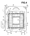
- Figure 4 is a bottom view of the IC socket 1.
- Figures 5A, 5B, and 5C illustrate a metal plate 100, which is to be attached to a socket housing, wherein Figure 5A is a plan view, Figure 5B is a front view, and Figure 5C is a side view.
- Figure 6 is a partial magnified view of a state prior to complete mounting of an IC package 200 onto the socket housing.
- Figure 7 is a partial magnified view of a state in which the IC package 200 is completely mounted.
- the IC socket 1 comprises: an insulative socket housing 2, which is formed by molding resin or the like; a cover member 8, which is rotatably mounted at or towards a first end 4 of the socket housing 2; a metallic reinforcing plate 10 (hereinafter, referred to simply as "reinforcing plate”), which is mounted at or towards a bottom of the socket housing 2; and a lever 12, which is axially supported at or towards a second end 6 of the socket housing 2.
- a substantially rectangular opening 68 is formed in the cover member 8.
- the lever 12 functions to lock the cover member 8 in its closed state.
- a great number of electrical contacts 90 are also provided in the socket housing 2 which are arranged substantially in a matrix. Note that an IC package 200, which is to be mounted onto the socket hosing 2, is partially illustrated in Figure 6 and Figure 7.
- the socket housing 2 is formed as a rectangular plate having a rectangular opening 22 at its center.
- a peripheral wall 24 made up by four sides is erected along the upper peripheral edges of the socket housing 2 to form an IC package receiving portion 26 which is upwardly opened.
- a substantially rectangular mounting portion 28 is integrally formed with the socket housing 2 at a lower portion thereof, corresponding to the IC package receiving portion 26.
- the opening 22 is capable of receiving the IC package 200, which is to be mounted in the IC package receiving portion 26, electronic components, such as capacitors mounted on a circuit board 150, and the like.
- Electrical contact apertures 32 are formed in a matrix through the bottom surface of the IC package receiving portion 26, that is, an IC package mounting surface 30 (refer to Figure 6 and Figure 7).
- the electrical contact apertures 32 penetrate through the mounting portion 28.
- the electrical contacts 90 are press fit and fixed within the electrical contact apertures 32.
- resilient contact pieces 90a protrude from the IC package mounting surface 30, as most clearly illustrated in Figure 6 and Figure 7.
- the contact pieces 90a contact conductive pads (electrical contacts, not shown) of the IC package 200.
- solder balls 90b which are to be soldered onto the circuit board 150, are exposed through the lower surface 38 of the socket housing 2.
- the reinforcing plate 10 which supports the socket housing 2 from below, will be described in detail.
- the reinforcing plate 10 is formed by punching and bending a single metal plate into a substantially rectangular frame, as illustrated most clearly in Figure 4.
- An opening 40 having a shape which is complementary to the shape of the mounting portion 28 of the socket housing 2, is formed approximately centered with respect to the reinforcing plate.
- the mounting portion 28 is provided within the opening 40 and protrudes downwardly from the reinforcing plate 10.
- the four sides of the reinforcing plate 10 are bent upwardly, to form a front wall 42, a rear wall 44, and side walls 46 and 48.
- Holding pieces 50 and 52 are integrally formed with the front wall 42 by inwardly bending the top of the front wall 42.
- the holding pieces 50 and 52 are separated from each other in the longitudinal direction of the front wall 42 and function to prevent rotating shafts 54 of lever 12 from being extracted.
- Front ends 46a and 48a of the side walls 46 and 48 are positioned beneath the rotating shafts 54 of lever 12, and cooperate with holding pieces 50 and 52 to axially support the rotating shafts 54 so that they are rotatable.
- Two rectangular openings 56 are formed in the rear wall 44 of the reinforcing plate 10.
- the openings 56 are separated from each other in the longitudinal direction of the rear wall 44.
- Support pieces 60 of cover member 8 are inserted into openings 56, to rotatably support the cover member 8.
- Four protrusions of socket housing 2 are thermally fused and fixed to opening 40 of the reinforcing plate 10 by swaging.
- the swaged portion is denoted by reference numeral 58 in Figure 4.
- a laterally protruding engaging protrusion 14 for fixing the lever 12 is formed on the side wall 46 of the reinforcing plate 10 (refer to Figure 1).
- the lever 12 is formed by bending a single metal wire, and comprises: the spaced rotating shafts 54, which are held by the holding pieces 50 and 52; a crank portion, which is a locking portion 62 positioned between and displaced from the rotating shafts 54; an operating rod 64; and an operating portion 66 for causing the rotating shafts 54 to rotate.
- the operating rod 64 is bent at a right angle with respect to the rotating shafts 54 in substantially the same direction as the displacement of the locking portion 62.
- the operating portion 66 is formed by bending the operating rod 64 in a U-shape.
- cover member 8 will be described. Note that in the description, the portion of the cover member 8 positioned toward the first end 4 of the IC socket 1 will be referred to as the "rear", and that the portion of the cover member 8 positioned toward the second end 6 will be referred to as the "front”.
- the cover member 8 is formed by punching and bending a single metal plate into a substantially rectangular shape.
- a locking piece 70 to be pressed and held by the locking portion 62, is formed at the center front portion of the cover member 8.
- the support pieces 60 which are inserted in the openings 56 of the reinforcing plate 10 to engage therewith, are formed on both lateral sides of the rear portion of the cover member 8.
- the support pieces 60 curve from bottom to top in an arcuate shape in a manner such that the engagement between the support pieces 60 and the openings 56 is not released when the cover member 8 rotates about the engaged portion.
- the side of the cover member 8, at which the support pieces 60 are formed is referred to as the "axial support side”
- the side of the cover member 8, at which the locking piece 70 is formed is referred to as the "engaging side”.
- the substantially rectangular opening 68 in which the IC package 200 is to be positioned, is formed at the central portion of the cover member 8. Note that the edges of the opening 68 are curved slightly downward, as illustrated in Figure 2. This is to facilitate control of the load applied onto the IC package 200 when the cover member 8 presses the IC package 200 against the IC socket 1. Cut-outs 69, which are formed in the opening 68 toward the side of the first end 4, are provided to eliminate interference between the cover member 8 and a flange 202 (refer to Figure 6) of the IC package during closing of cover member 8. By eliminating the interference, the locking portion 62 and the locking piece 70 are capable of a positive engagement.
- a metal plate 100 which is mounted onto the socket housing 2, will be described.
- a pair of metal plates 100 are mounted on a peripheral wall 24a, which is the portion of the rectangular peripheral wall 24 positioned at or towards the second end 6.
- the metal plates 100 extend from an upper surface 118 of the peripheral wall 24a along an inner surface 102 thereof.
- the metal plates 100 are separated in the direction of the peripheral wall 24a.
- the metal plates 100 will be described with reference to Figures 5A, 5B, and 5C.
- the state in which the metal plates 100 are mounted onto the socket housing 2 will be described with reference to Figure 6 and Figure 7.
- each metal plate 100 is formed by punching and bending a single metallic plate of stainless steel, a copper alloy or the like.
- the metal plate 100 has a smooth surface and comprises: a substantially rectangular main plate portion 104 (vertical portion); a protective plate portion 106 (horizontal portion), which is bent at a right angle with respect to the main plate portion 104; and a curved portion 108 (guide portion) for connecting the main plate portion 104 and the protective plate portion 106.
- the upper end portion of the main plate portion 104 is relatively wide. Lateral edges 112 extend downwardly from the bottom of the wide upper portion to the lower end 110 of the metal plate 100.
- a barb 114 is formed on each lateral edge 112, and bevels 116 are formed at the lower corners thereof.
- the protective plate portion 106 is of a substantially rectangular shape, wherein the sides corresponding to the width direction of the metal plate 100 are the long sides, and the sides in the bending direction are the short sides of the rectangle.
- Mounting grooves 120 are formed in the upper surface 118 and the inner surface 102 of the peripheral wall 24a at positions corresponding to the metal plates 100.
- the mounting grooves 120 have a depth which substantially equals the plate thickness of the metal plates 100, and have a shape which is complementary thereto. Accordingly, when the metal plates 100 are press fit into the mounting grooves 120, the protective plate portions 106 become substantially coplanar with the upper surface 118, and the main plate portions 104 become substantially coplanar with the inner surface 102. However, the protective plate portions 106 may protrude upwardly from the upper surface 118, and the main plate portions 104 may protrude inwardly from the inner surface 102.
- lever 12 illustrated in Figure 1 is released from the engaging protrusions 14 and rotated 90° toward the surface of the drawing sheet of Figure 1.
- the rotation causes the locking portions 62 of lever 12 and the cover member 8 to become disengaged, thereby enabling rotation of the cover member 8 about its axial support portion.
- the IC package 200 is placed on the socket housing 2, as illustrated in Figure 6.
- the cover member 8 is closed, the lever 12 is rotated so that the locking portions 62 thereof press and fix the locking pieces 70 of the cover member 8.
- the upper surface of the flange 202 of the IC package 200 is pressed by the downwardly curved surface of the cover member 8.
- the IC package 200 is fixed to the socket housing 2 in this manner. However, there are cases in which the IC package 200 is erroneously placed on the socket housing 2 at a position shifted from its proper position. There are also cases in which the IC package 200 is moved during closing of the cover member 8. Referring to Figure 6, if the cover member 8 (omitted from Figure 6) is pressed while the IC package, illustrated by broken lines, is in the position denoted by reference numeral 200', downward movement of the edge 204 of the IC package 200 is prevented by the protective plate portions 106 of the metal plates 100. Accordingly, the upper surface 118 is not ground down by an edge 204 of the IC package 200.
- the edge 204 is positioned on the curved portions 108 of the metal plates 100, the IC package 200, which is pressed from above, is guided toward the mounting surface 30 along the curved surfaces of the curved portions 108. Thereby, the IC package is positioned at the position denoted by reference numeral 200.
Landscapes
- Engineering & Computer Science (AREA)
- Microelectronics & Electronic Packaging (AREA)
- Connecting Device With Holders (AREA)
Applications Claiming Priority (2)
| Application Number | Priority Date | Filing Date | Title |
|---|---|---|---|
| JP2004070546 | 2004-03-12 | ||
| JP2004070546A JP4493006B2 (ja) | 2004-03-12 | 2004-03-12 | Icソケット |
Publications (2)
| Publication Number | Publication Date |
|---|---|
| EP1575346A2 true EP1575346A2 (de) | 2005-09-14 |
| EP1575346A3 EP1575346A3 (de) | 2007-08-08 |
Family
ID=34824624
Family Applications (1)
| Application Number | Title | Priority Date | Filing Date |
|---|---|---|---|
| EP05101616A Withdrawn EP1575346A3 (de) | 2004-03-12 | 2005-03-02 | IC-Fassung |
Country Status (5)
| Country | Link |
|---|---|
| US (1) | US7125259B2 (de) |
| EP (1) | EP1575346A3 (de) |
| JP (1) | JP4493006B2 (de) |
| CN (1) | CN100466400C (de) |
| TW (1) | TWM283402U (de) |
Families Citing this family (7)
| Publication number | Priority date | Publication date | Assignee | Title |
|---|---|---|---|---|
| JP4319574B2 (ja) * | 2004-04-14 | 2009-08-26 | タイコエレクトロニクスアンプ株式会社 | Icソケット |
| US7374446B2 (en) * | 2004-04-14 | 2008-05-20 | Tyco Electronics Amp K.K | IC socket |
| CN200959469Y (zh) * | 2006-09-08 | 2007-10-10 | 富士康(昆山)电脑接插件有限公司 | 电连接器 |
| CN201072829Y (zh) * | 2007-06-11 | 2008-06-11 | 富士康(昆山)电脑接插件有限公司 | 电连接器 |
| CN103380550B (zh) * | 2011-02-28 | 2015-11-25 | 惠普发展公司,有限责任合伙企业 | 弹簧加载盖 |
| TWI583068B (zh) * | 2012-08-02 | 2017-05-11 | 鴻海精密工業股份有限公司 | 電連接器 |
| CN109842788B (zh) * | 2019-01-15 | 2020-10-30 | 浙江金果知识产权有限公司 | 基于物联网的交通工具的集成电路监控装置 |
Family Cites Families (18)
| Publication number | Priority date | Publication date | Assignee | Title |
|---|---|---|---|---|
| JPH02230673A (ja) * | 1989-03-03 | 1990-09-13 | Mitsubishi Electric Corp | 半導体ソケツト |
| JP3572795B2 (ja) * | 1996-04-22 | 2004-10-06 | 株式会社エンプラス | Icソケット |
| US6086387A (en) * | 1998-05-14 | 2000-07-11 | International Business Machines Corporation | Cover assembly for a socket adaptable to IC modules of varying thickness used for burn-in testing |
| DE69800330T2 (de) * | 1998-07-30 | 2001-05-17 | Molex Inc., Lisle | IC-Kartenverbinder |
| JP2000133397A (ja) * | 1998-10-22 | 2000-05-12 | Ace Five:Kk | コネクタ装置 |
| JP2000241500A (ja) * | 1998-12-22 | 2000-09-08 | Fujitsu Ltd | 半導体装置用ソケットの取付構造 |
| JP2004514142A (ja) * | 2000-11-17 | 2004-05-13 | コーニンクレッカ フィリップス エレクトロニクス エヌ ヴィ | 部品の検査ic用ソケット及び部品のic検査方法 |
| JP2003168531A (ja) * | 2001-11-30 | 2003-06-13 | Enplas Corp | 電気部品用ソケット |
| US6508659B1 (en) * | 2002-03-01 | 2003-01-21 | Hon Hai Precision Ind. Co., Ltd. | Electrical socket having a backup means |
| TW537511U (en) * | 2002-07-26 | 2003-06-11 | Hon Hai Prec Ind Co Ltd | An electronic connector device |
| TW560718U (en) * | 2002-11-15 | 2003-11-01 | Hon Hai Prec Ind Co Ltd | Electrical connector |
| TW549644U (en) * | 2002-12-13 | 2003-08-21 | Hon Hai Prec Ind Co Ltd | Electrical connector |
| TW551635U (en) * | 2002-12-13 | 2003-09-01 | Hon Hai Prec Ind Co Ltd | Electrical connector |
| TW551640U (en) * | 2002-12-17 | 2003-09-01 | Hon Hai Prec Ind Co Ltd | Electrical connector |
| TW549635U (en) * | 2002-12-20 | 2003-08-21 | Hon Hai Prec Ind Co Ltd | Strengthened belectrical connector |
| US6916195B2 (en) * | 2003-03-26 | 2005-07-12 | Intel Corporation | Land grid array socket loading device |
| US6722909B1 (en) * | 2003-04-17 | 2004-04-20 | Hon Hai Precision Ind. Co., Ltd. | Electrical connector with lever retainer |
| JP4273495B2 (ja) * | 2004-03-25 | 2009-06-03 | Smk株式会社 | 電子部品取付用ソケット |
-
2004
- 2004-03-12 JP JP2004070546A patent/JP4493006B2/ja not_active Expired - Fee Related
-
2005
- 2005-03-02 EP EP05101616A patent/EP1575346A3/de not_active Withdrawn
- 2005-03-09 TW TW094203638U patent/TWM283402U/zh not_active IP Right Cessation
- 2005-03-11 US US11/078,076 patent/US7125259B2/en not_active Expired - Lifetime
- 2005-03-14 CN CNB2005100547122A patent/CN100466400C/zh not_active Expired - Fee Related
Also Published As
| Publication number | Publication date |
|---|---|
| US7125259B2 (en) | 2006-10-24 |
| EP1575346A3 (de) | 2007-08-08 |
| US20050202708A1 (en) | 2005-09-15 |
| TWM283402U (en) | 2005-12-11 |
| CN100466400C (zh) | 2009-03-04 |
| JP4493006B2 (ja) | 2010-06-30 |
| JP2005259572A (ja) | 2005-09-22 |
| CN1667889A (zh) | 2005-09-14 |
Similar Documents
| Publication | Publication Date | Title |
|---|---|---|
| US7101210B2 (en) | LGA socket | |
| US8979565B2 (en) | Electrical connector having a holding member and a load plate pivotally assembled to two ends of a stiffener | |
| US9780473B2 (en) | Mating connector using slider to deform contacts | |
| KR20050040810A (ko) | 카드용 커넥터 | |
| US20070202750A1 (en) | Card connector | |
| EP1575346A2 (de) | IC-Fassung | |
| US20080037236A1 (en) | IC Package, IC Socket, and IC Socket Assembly | |
| US7828565B2 (en) | Electrical connector assembly with pick up cap | |
| US8092242B2 (en) | Socket with an easily operated cover | |
| TWI466396B (zh) | Electrical connectors for circuit boards | |
| US7690926B2 (en) | Electrical connector assembly with stiffener | |
| TW200308128A (en) | Production method of flat cable connector | |
| US7867004B2 (en) | Electrical connector with improved stiffener device | |
| EP1585051B1 (de) | Kartenverbinder mit einem Verriegelungselement zur Verriegelung eines Abdeckungselements verwendet zur Massenverbindung | |
| US7753707B1 (en) | Electrical connecting assembly | |
| CN102347535A (zh) | 存储卡用连接器 | |
| US7950937B2 (en) | Card connector with bulge portion | |
| US7014489B2 (en) | Land grid array connector assembly | |
| US7078622B2 (en) | IC socket assembly | |
| US6540541B2 (en) | ZIF socket assembly having protector placed on chip mounted on the socket assembly | |
| US8251726B2 (en) | Electrical connector having a metal frame with locking portions movable in transverse direction for locking/unlocking a card | |
| CN102437468A (zh) | 连接器 | |
| JPH0525634U (ja) | スライドスイツチ | |
| JPH0584070U (ja) | 押し付け接続兼揺動形コネクタ |
Legal Events
| Date | Code | Title | Description |
|---|---|---|---|
| PUAI | Public reference made under article 153(3) epc to a published international application that has entered the european phase |
Free format text: ORIGINAL CODE: 0009012 |
|
| AK | Designated contracting states |
Kind code of ref document: A2 Designated state(s): AT BE BG CH CY CZ DE DK EE ES FI FR GB GR HU IE IS IT LI LT LU MC NL PL PT RO SE SI SK TR |
|
| AX | Request for extension of the european patent |
Extension state: AL BA HR LV MK YU |
|
| PUAL | Search report despatched |
Free format text: ORIGINAL CODE: 0009013 |
|
| AK | Designated contracting states |
Kind code of ref document: A3 Designated state(s): AT BE BG CH CY CZ DE DK EE ES FI FR GB GR HU IE IS IT LI LT LU MC NL PL PT RO SE SI SK TR |
|
| AX | Request for extension of the european patent |
Extension state: AL BA HR LV MK YU |
|
| 17P | Request for examination filed |
Effective date: 20080115 |
|
| AKX | Designation fees paid |
Designated state(s): DE FR GB NL |
|
| 17Q | First examination report despatched |
Effective date: 20091211 |
|
| STAA | Information on the status of an ep patent application or granted ep patent |
Free format text: STATUS: THE APPLICATION IS DEEMED TO BE WITHDRAWN |
|
| 18D | Application deemed to be withdrawn |
Effective date: 20100422 |