EP1576726B1 - Zusammengesetzte verstärkerstruktur - Google Patents
Zusammengesetzte verstärkerstruktur Download PDFInfo
- Publication number
- EP1576726B1 EP1576726B1 EP02793732A EP02793732A EP1576726B1 EP 1576726 B1 EP1576726 B1 EP 1576726B1 EP 02793732 A EP02793732 A EP 02793732A EP 02793732 A EP02793732 A EP 02793732A EP 1576726 B1 EP1576726 B1 EP 1576726B1
- Authority
- EP
- European Patent Office
- Prior art keywords
- amplifier
- driving
- composite
- amplifier structure
- dynamic range
- Prior art date
- Legal status (The legal status is an assumption and is not a legal conclusion. Google has not performed a legal analysis and makes no representation as to the accuracy of the status listed.)
- Expired - Lifetime
Links
- 239000002131 composite material Substances 0.000 title claims abstract description 58
- 238000000034 method Methods 0.000 claims description 17
- 230000001419 dependent effect Effects 0.000 claims description 5
- 238000010586 diagram Methods 0.000 description 29
- 230000005540 biological transmission Effects 0.000 description 16
- 230000007704 transition Effects 0.000 description 12
- 239000000470 constituent Substances 0.000 description 6
- 230000008901 benefit Effects 0.000 description 5
- 230000008859 change Effects 0.000 description 4
- 238000009826 distribution Methods 0.000 description 3
- 230000004048 modification Effects 0.000 description 3
- 238000012986 modification Methods 0.000 description 3
- 230000003321 amplification Effects 0.000 description 2
- 239000003990 capacitor Substances 0.000 description 2
- 230000001413 cellular effect Effects 0.000 description 2
- 238000006243 chemical reaction Methods 0.000 description 2
- 238000003199 nucleic acid amplification method Methods 0.000 description 2
- 238000006467 substitution reaction Methods 0.000 description 2
- 230000009466 transformation Effects 0.000 description 2
- 230000001131 transforming effect Effects 0.000 description 2
- 238000004891 communication Methods 0.000 description 1
- 238000001816 cooling Methods 0.000 description 1
- 238000003780 insertion Methods 0.000 description 1
- 230000037431 insertion Effects 0.000 description 1
- 230000002452 interceptive effect Effects 0.000 description 1
- 238000012886 linear function Methods 0.000 description 1
- 239000000203 mixture Substances 0.000 description 1
- 230000004044 response Effects 0.000 description 1
- 238000000844 transformation Methods 0.000 description 1
Images






Classifications
-
- H—ELECTRICITY
- H03—ELECTRONIC CIRCUITRY
- H03F—AMPLIFIERS
- H03F1/00—Details of amplifiers with only discharge tubes, only semiconductor devices or only unspecified devices as amplifying elements
- H03F1/32—Modifications of amplifiers to reduce non-linear distortion
-
- H—ELECTRICITY
- H03—ELECTRONIC CIRCUITRY
- H03F—AMPLIFIERS
- H03F1/00—Details of amplifiers with only discharge tubes, only semiconductor devices or only unspecified devices as amplifying elements
- H03F1/02—Modifications of amplifiers to raise the efficiency, e.g. gliding Class A stages, use of an auxiliary oscillation
- H03F1/0205—Modifications of amplifiers to raise the efficiency, e.g. gliding Class A stages, use of an auxiliary oscillation in transistor amplifiers
-
- H—ELECTRICITY
- H03—ELECTRONIC CIRCUITRY
- H03F—AMPLIFIERS
- H03F1/00—Details of amplifiers with only discharge tubes, only semiconductor devices or only unspecified devices as amplifying elements
- H03F1/02—Modifications of amplifiers to raise the efficiency, e.g. gliding Class A stages, use of an auxiliary oscillation
- H03F1/0205—Modifications of amplifiers to raise the efficiency, e.g. gliding Class A stages, use of an auxiliary oscillation in transistor amplifiers
- H03F1/0288—Modifications of amplifiers to raise the efficiency, e.g. gliding Class A stages, use of an auxiliary oscillation in transistor amplifiers using a main and one or several auxiliary peaking amplifiers whereby the load is connected to the main amplifier using an impedance inverter, e.g. Doherty amplifiers
-
- H—ELECTRICITY
- H03—ELECTRONIC CIRCUITRY
- H03F—AMPLIFIERS
- H03F1/00—Details of amplifiers with only discharge tubes, only semiconductor devices or only unspecified devices as amplifying elements
- H03F1/02—Modifications of amplifiers to raise the efficiency, e.g. gliding Class A stages, use of an auxiliary oscillation
- H03F1/0205—Modifications of amplifiers to raise the efficiency, e.g. gliding Class A stages, use of an auxiliary oscillation in transistor amplifiers
- H03F1/0294—Modifications of amplifiers to raise the efficiency, e.g. gliding Class A stages, use of an auxiliary oscillation in transistor amplifiers using vector summing of two or more constant amplitude phase-modulated signals
-
- H—ELECTRICITY
- H03—ELECTRONIC CIRCUITRY
- H03F—AMPLIFIERS
- H03F3/00—Amplifiers with only discharge tubes or only semiconductor devices as amplifying elements
- H03F3/20—Power amplifiers, e.g. Class B amplifiers, Class C amplifiers
- H03F3/24—Power amplifiers, e.g. Class B amplifiers, Class C amplifiers of transmitter output stages
-
- H—ELECTRICITY
- H03—ELECTRONIC CIRCUITRY
- H03F—AMPLIFIERS
- H03F3/00—Amplifiers with only discharge tubes or only semiconductor devices as amplifying elements
- H03F3/60—Amplifiers in which coupling networks have distributed constants, e.g. with waveguide resonators
-
- H—ELECTRICITY
- H03—ELECTRONIC CIRCUITRY
- H03F—AMPLIFIERS
- H03F3/00—Amplifiers with only discharge tubes or only semiconductor devices as amplifying elements
- H03F3/60—Amplifiers in which coupling networks have distributed constants, e.g. with waveguide resonators
- H03F3/602—Combinations of several amplifiers
-
- H—ELECTRICITY
- H03—ELECTRONIC CIRCUITRY
- H03F—AMPLIFIERS
- H03F3/00—Amplifiers with only discharge tubes or only semiconductor devices as amplifying elements
- H03F3/60—Amplifiers in which coupling networks have distributed constants, e.g. with waveguide resonators
- H03F3/602—Combinations of several amplifiers
- H03F3/604—Combinations of several amplifiers using FET's
-
- H—ELECTRICITY
- H03—ELECTRONIC CIRCUITRY
- H03F—AMPLIFIERS
- H03F2200/00—Indexing scheme relating to amplifiers
- H03F2200/423—Amplifier output adaptation especially for transmission line coupling purposes, e.g. impedance adaptation
-
- H—ELECTRICITY
- H03—ELECTRONIC CIRCUITRY
- H03F—AMPLIFIERS
- H03F2200/00—Indexing scheme relating to amplifiers
- H03F2200/543—A transmission line being used as coupling element between two amplifying stages
Definitions
- the present invention relates generally to an improved composite amplifier structure and a method of driving such an amplifier.
- the invention also relates to a radio terminal including such a structure.
- the power amplifier (PA) in the transmitter has to be very linear, in addition to being able to simultaneously amplify many radio channels (frequencies) or independent user data channels, spread across a fairly wide bandwidth. It also has to do this efficiently, to reduce power consumption, need for cooling, and to increase its longevity. High linearity is required since nonlinear amplifiers would cause leakage of interfering signal energy between channels and distortion within each channel.
- the amplitude probability density of a mix of sufficiently many independent radio frequency (RF) channels, or of a multi-user CDMA (Code Division Multiple Access) signal tends to be close to a Rayleigh distribution having a large peak-to-average power ratio. Since a conventional linear RF power amplifier generally has an efficiency proportional to its output amplitude, its average efficiency is very low for such signals.
- the Doherty amplifier uses one nonlinear and one linear amplifier.
- a first power amplifier is driven as a linear amplifier in class B, and a second power amplifier having nonlinear output current "modulates" the impedance seen by the first amplifier, through an impedance-inverting quarter-wave line [1, 3]. Since the nonlinear output current of the second amplifier is zero below a certain transition (output) voltage, the second amplifier does not contribute to the power loss below this voltage.
- the standard Doherty amplifier's transition point (which corresponds to a maximum in the efficiency curve) is at half the maximum output voltage.
- the location of the transition point can be changed by changing the impedance of the quarter-wave transmission line (or equivalent circuit). Different size (power capacity) amplifiers will then be needed for optimum utilization of the available peak power.
- the Doherty system can be extended to three or more amplifiers, to obtain more maximum points on the efficiency curve. This usually leads to a requirement for very unevenly sized amplifiers (i.e. transistors).
- outphasing which is the key method in Chireix and LINC amplifiers, generally means the method of obtaining amplitude modulation by combining several (generally two) phase-modulated constant-amplitude signals. These signals are produced in a "signal component separator” (SCS) and subsequently, after up-conversion and amplification through RF chains (mixers filters and amplifiers), combined to form an amplified linear signal in an output combiner network.
- SCS signal component separator
- RF chains mixer filters and amplifiers
- the phases of these constant-amplitude signals are chosen so that the result from their vector-summation yields the desired amplitude.
- the compensating reactances +jX and -jX in the output network of the Chireix amplifier are used to extend the region of high efficiency to include lower output power levels.
- the efficiency of Chireix systems are derived in [4, 5].
- Chireix amplifier An advantage of the Chireix amplifier is the ability to change the efficiency curve to suit different peak-to-average power ratios, by changing the size (X) of the reactances.
- the peak output power is equally divided between the amplifiers irrespective of this adjustment, which means that equal size amplifiers can be used.
- An object of the present invention is to provide an efficient multi-stage composite power amplifier structure and a method for driving such a structure.
- a further object is a radio terminal including such a structure.
- the present invention suggests an efficient composite amplifier structure, which essentially is based on a combination of the auxiliary amplifier of a Doherty amplifier and at least one pair of amplifiers forming a Chireix pair.
- the Doherty part of the composite amplifier is driven in the same manner as the auxiliary amplifier of a Doherty amplifier.
- Each Chireix pair is driven by drive signals having amplitude dependent phase over at least a part of the dynamic range of the composite amplifier.
- Preferably different pairs have amplitude dependent phase in different parts of the dynamic range to maximize efficiency.
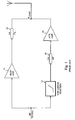
- Fig. 1 is a block diagram of a typical prior art Doherty amplifier.
- the Doherty amplifier uses one linear and one nonlinear power amplifier.
- the published theory states that a main power amplifier 10 is driven as a linear amplifier in class B, and an auxiliary power amplifier 12 having nonlinear output current (through class C operation or some other technique represented by block 14) "modulates" the impedance seen by the main amplifier, through an impedance-inverting quarter-wave line 16 in the output network.
- the input path to the auxiliary amplifier also contains a 90° phase shifter 18. Since the nonlinear output current of the auxiliary amplifier is zero below a certain transition (output) voltage, the auxiliary amplifier does not contribute to the power loss below this voltage.
- the transition point of the standard Doherty amplifier is at half the maximum output voltage. With this transition point the efficiency curve is most suited for moderate peak-to-average power ratios, and the peak power is divided equally between the two constituent amplifiers.
- the transition point in the Doherty amplifier can be changed by changing the impedance of the quarter-wave transmission line (or equivalent circuit). The efficiency curve can then be adjusted for higher peak-to-average power ratios, and the peak output power will be unequally divided between the amplifiers. Different size (power capacity) amplifiers will thus be needed for optimum utilization of the available peak power.
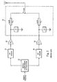
- Fig. 2 is a block diagram of a typical prior art Chireix amplifier.
- Output network 32 includes two quarter-wave lines ⁇ /4 (where ⁇ is the wavelength of the center frequency of the frequency band at which the amplifier is operated) and two compensating reactances +jX and -jX, which are used to extend the region of high efficiency to include lower output power levels.
- Chireix amplifier An advantage of the Chireix amplifier is the ability to change the efficiency curve to suit different peak-to-average power ratios, by changing the size (X) of the reactances.
- the peak output power is equally divided between the amplifiers irrespective of this adjustment, which means that equal size (power capacity) amplifiers can be used.
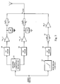
- Fig. 3 is a block diagram of an exemplary embodiment of a composite amplifier in accordance with the present invention.
- this embodiment essentially is a combination of a Chireix amplifier (including power amplifiers PA 1,1 and PA 1,2) with an auxiliary amplifier PA 2 of a Doherty amplifier.
- a slight modification in the "Doherty part" is that the non-linear function is implemented in the baseband (for example as a lookup table and a D/A converter) instead of the RF band. For this reason a further RF chain 28 has been included in the input network.
- the Chireix part signal component separator 22 is modified to generate outphased signals only in a certain region of the dynamic range of the composite amplifier structure.
- the illustrated composite amplifier structure can be substituted for a single stand-alone amplifier, for example a class B (AB) linear RF amplifier or for one of the amplifiers in a Doherty system, provided the three amplifiers together have the same maximum output current as the amplifier they replace.
- AB class B
- the composite amplifier structure in accordance with the present invention may be part of a transmitter, for example a transmitter in a radio terminal, such as a base station or a mobile station in a cellular mobile radio communication system.
- a radio terminal such as a base station or a mobile station in a cellular mobile radio communication system.
- the composite amplifier in Fig. 3 includes a semi-lumped output network using quarter-wave transmission lines together with inductors (+jX) and capacitors (-jX). Another possibility is a distributed output network illustrated in Fig. 4 . This structure uses only shortened and lengthened transmission lines. Another example is illustrated in Fig. 5 . A half-wavelength transmission line from PA 2 is included in Fig. 5 for illustrative purposes; any number of half wavelengths of transmission line can be added to any of the amplifiers, with a corresponding change in the phase of the drive signal to that amplifier.
- the Chireix part of the output network may be describes as including impedance inverting elements corresponding a total line length of ⁇ /2 or lengthened and shortened elements having an average line length of ⁇ /4.
- the quarter-wave lines can also be used for transforming between the load and the transistors. More impedance-matching sections can also be used in each branch, and many other circuit transformation techniques are available.
- the transmission line impedances should be substantially equal to the optimal load resistance of each constituent amplifier. If the structure is used by itself, as a three-amplifier system, the transformed antenna impedance R LOAD , connected at the denoted connection point, should equal the parallel connection of the optimal loads of all three constituent amplifiers.
- Fig. 3 may in principle be driven as a combination of a classical Chireix outphasing mode for PA 1,1 and PA 1,2 and a non-linear Doherty mode for PA 2, more efficient drive modes will now be described.
- the improved operation of a three-amplifier system can be subdivided into three main regions.
- PA 1,1 and PA 1,2 are driven to supply linearly increasing (with respect to the output amplitude) currents with a constant phase angle between them.
- the upper boundary of this region is determined by the size of the reactances, X ( Fig. 3 ), or equivalently, by the line length difference ⁇ ( Fig. 4 ).
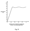
- This parameter is usually chosen so that the average efficiency is maximized for the signal amplitude distribution used, by placing the lowermost efficiency maximum (see Fig. 10 ) at a certain output amplitude point.
- the same two amplifiers are driven in an outphasing fashion, with constant amplitudes and varying relative phase of their output node voltages.
- the upper boundary of the middle region is determined by the relation between the sum of the maximum output powers of PA 1,1 and PA 1,2 to the sum of all three amplifiers' maximum output power.
- PA 1,1 and PA 1,2 are held at constant voltage and constant phase difference while together supplying a substantially linearly increasing output current.
- the third amplifier PA 2 is also active, supplying a linearly increasing current starting from zero.
- the amplitudes and phases of the voltages at the output nodes of then amplifiers are shown in Fig. 6 and Fig. 7 , respectively.
- the voltage at PA 2 contains the desired output signal, which implies that its amplitude rises linearly with the output amplitude, while the voltages at PA 1,1 and PA 1,2 rise faster at low output amplitudes (up to about 0.23 of the maximum output amplitude), and are held constant at higher amplitudes.
- the phase of the voltage at PA 2 is the desired output signal phase.
- PA 1,1 and PA 1,2 start out, at low output amplitudes, with a constant relative phase difference, and constant offset to the phase of the output signal. From 0.23 to 0.67 of the maximum output amplitude, PA 1,1 and PA 1,2 operate in an outphasing fashion, and at output levels above 0.67 they have constant phase relative to the output.
- Fig. 8 and Fig. 9 The amplitudes and phases of the RF currents delivered by the amplifiers are shown in Fig. 8 and Fig. 9 , respectively.
- PA 1,1 and PA 1,2 deliver linear currents with constant phases, relative to the output, at low amplitudes. In the middle amplitude region these amplifiers are in an outphasing mode. At high output amplitudes, PA 2 is also active, while PA 1,1 and PA 1,2 continue to increase their output currents. In this region, the relative phases need to change, albeit less than in the outphasing region, to obtain optimal efficiency.
- the absence of a phase plot for PA 2 at low output amplitudes indicates that this is a "don't care" region, since the delivered current is zero anyway.
- the resulting efficiency for the three-amplifier system assuming linear transistors in class B operation, is shown in Fig. 10 .
- a difference between operating the described structure within a Doherty system and operating it as a single stand-alone high-efficiency amplifier is that the choice of reactance value, or equivalently, line length difference, has new restrictions. These restrictions depend on which power amplifier in the Doherty system is replaced, since the different amplifiers in the Doherty system operate differently in the different regions of operation.
- the amplifiers in the Doherty system all start (at an output level of zero, for the first or main amplifier, or at a so called transition point at a higher output amplitude, for subsequent or auxiliary amplifiers) by delivering linear current (as a function of output voltage). In the region above the next transition point, the voltage amplitude at an amplifier's output node is constant, while it continues to deliver linear current.
- the current amplitude is also constant.
- the reactance value or line length difference must be chosen so that it gives efficient outphasing operation in (usually the lower part of) the lowest active region of the replaced amplifier (where the original amplifier delivered linear current).
- the division of the maximum output power between the constituent amplifiers also has new considerations. If there is an amplifier whose active region starts at a transition point above that of the substituted amplifier, only the constituent amplifier which is not outphasing will continue to deliver linear current in this higher region. This means that the division of output power between the amplifiers at maximum output amplitude is not the same as the division of power at the transition point. This in turn has the implication that the division of maximum output power between the amplifiers in the multi-amplifier building block must take into consideration the placement of the transition points in the original Doherty structure.
- the transmission line impedances that are used in the building block are equal to the optimal load resistance of the respective amplifiers.
- the rest of the amplifiers, as well as the transmission lines (or equivalent networks), that are used in the original Doherty system, remain unaffected by the substitution.
- the current delivered, the output node voltages, the dimensioning, everything stays the same. This also means that multiple insertions of the new building blocks can be made in the same original Doherty amplifier.
- the basic three-amplifier structure as a building block for replacing the second amplifier in a three-stage Doherty system, shown in Fig. 11 .
- the resulting structure looks like the one shown in Fig, 12 .
- the amplifier PA 2 indicated by the dashed block in Fig. 11 has been replaced by the three-amplifier structure indicated by the dashed block in Fig, 12 .
- the output power capability of PA 2 in the original Doherty system is divided between the three partial amplifiers PA 2,1, PA 2,2 and PA 2,3 of the new system.
- PA 1 and PA 3 operate in the same way in both the original Doherty system and the new system.
- the transformed antenna impedance, R LOAD 0.2 times the optimal load of PA 3.
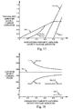
- Fig. 13 The amplitudes of the RF currents from the constituent amplifiers of the three-stage Doherty system of Fig. 11 are shown in Fig. 13 .
- the currents of the lower stages are normalized to the maximum output current of PA 3.
- the resulting efficiency of this reference system is shown in Fig. 14 .
- Fig. 15 and Fig. 16 the amplitudes and phases of the RF voltages at the output nodes of the amplifiers are shown.
- the output voltage at PA 3 is used as the phase reference for the other amplifiers.
- PA 1, PA 2,1 and PA 2,2 all deliver a maximum output current of 0.8 times that of PA 3.
- PA 2,3 delivers maximally twice that amount, i.e. 1.6 times that of PA 3. If we add the maximum currents of the amplifiers replacing PA 2 in the original Doherty system, we arrive at 3.2 times the maximum current of PA 3, which is the same as the maximum of the PA 2 output current in the original system. Note that the shape and size of the output current amplitude plots of PA 1 and PA 3 are identical to those of the original system as shown in Fig. 13 .
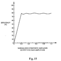
- the three-amplifier system described so far can be expanded to any odd number of amplifiers, by essentially using a multi-stage Chireix structure in place of the single (two-amplifier) structure used so far. This has the benefit of further increasing efficiency.
- the order in which the different stages within an amplifier or building block operate in outphasing mode is determined by the size of the reactances.
- the division of the maximum output power between the Chireix part and the single (remaining) amplifier in the new multi-amplifier system follows the same considerations irrespective of the choice of single or multiple Chireix pairs in the system.
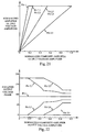
- the amplitudes and phases of the voltages at the output nodes of the amplifiers are shown in Fig. 21 and Fig. 22 , respectively.
- the voltage at PA 2,5 contains the amplitude and phase of the desired output signal.
- the voltage at PA 1 leads the output by 90°, and is the first to reach its maximum.
- the two "Chireix pairs" PA 2,1 + PA 2,2 and PA 2,3 + PA 2,4 operate in outphasing mode during different regions of output amplitude, and have constant phase relative to the output in the uppermost sixth of the output amplitude range.
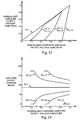
- Fig. 23 and Fig. 24 The amplitudes and phases of the currents are shown in Fig. 23 and Fig. 24 , respectively.
- the phase plots are only shown for the region in which each amplifier is active (delivering current).
- PA 1 is active during all output levels, as expected from the first stage of a two-amplifier Doherty system.
- the two "Chireix pairs" are active above approximately 0.17 and 0.47 of the output amplitude, respectively.
- PA 2,5 is active in the uppermost sixth of the output amplitude range.
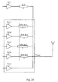
- the described efficient modes may, for example, be implemented by an amplifier input network in accordance with Fig. 26 .
- a digital input signal IN is forwarded to a vector lookup table 40, where a single input signal value generates an output signal vector.
- Each vector component is then forwarded to a D/A converter 42 and thereafter to the respective RF chain 44. This transforms the digital input signal amplitude into the proper drive signals (the input signal amplitude is assumed to be proportional to the composite amplifier output voltage amplitude).
- the invention By use of the invention as a stand-alone amplifier, it is possible to obtain higher efficiency than with multi-stage Doherty networks with the same number of transistors (amplifiers). This is because more of the peaks in the efficiency curve are flat (rounded) rather than peaked (as in the classical Doherty case).
- the invention is, for many commonly occurring signal amplitude distributions, more efficient than prior systems consisting of an odd number of amplifiers.
- Another advantage is that more evenly sized (and possibly equal size) transistors can be used, as compared to a Doherty amplifier. This is useful, since often only a limited number of transistor sizes are available from the manufacturers.
Landscapes
- Engineering & Computer Science (AREA)
- Power Engineering (AREA)
- Physics & Mathematics (AREA)
- Nonlinear Science (AREA)
- Amplifiers (AREA)
Claims (25)
- Komposit-Leistungsverstärkerstruktur, gekennzeichnet durch:einen ersten Leistungsverstärker (PA2), der als ein Hilfsverstärker eines Doherty-Verstärkers konfiguriert ist und mit einem Ausgangsknoten verbunden ist; undeine gerade Anzahl von weiteren Leistungsverstärkern, die in zumindest einem Chireix-Paar (PA 1, 1 PA 1, 2) konfiguriert sind, das mit dem Ausgangsknoten verbunden ist.
- Verstärkerstruktur nach Anspruch 1, gekennzeichnet durch eine Vorrichtung (40) zum Ansteuern zumindest eines Chireix-Paares durch Ansteuersignale mit einer Amplituden-abhängigen Phase über zumindest einen Teil des Dynamikbereichs der Kompositverstärkerstruktur.
- Verstärkerstruktur nach Anspruch 2, gekennzeichnet durch eine Vorrichtung (40) zum Ansteuern zumindest eines Chireix-Paares in einem Außerphasenmodus (Outphasing Mode) über zumindest einen Teil des Dynamikbereiches der Kompositverstärkerstruktur.
- Verstärkerstruktur nach Anspruch 3, gekennzeichnet durch eine Vorrichtung (40) zum Ansteuern zumindest zweier Chireix-Paare in einem Außerphasenmodus über unterschiedliche Teile des Dynamikbereichs der Kompositverstärkerstruktur.
- Verstärkerstruktur nach Anspruch 3, gekennzeichnet durch eine Vorrichtung (40) zum Ansteuern zumindest eines Chireix-Paares mit im Wesentlichen linearen Stromamplituden oberhalb seines entsprechenden Außerphasenteiles des Dynamikbereichs der Kompositverstärkerstruktur.
- Verstärkerstruktur nach Anspruch 3, gekennzeichnet durch eine Vorrichtung (40) zum Ansteuern zumindest eines Chireix-Paares mit im Wesentlichen linearen Stromamplituden unterhalb seines entsprechenden Außerphasenteiles des Dynamikbereichs der Kompositverstärkerstruktur.
- Verstärkerstruktur nach Anspruch 1, gekennzeichnet durch eine Vorrichtung (40) zum Ansteuern des ersten Leistungsverstärkers (PA2) mit im Wesentlichen Nullstromamplituden unterhalb und im Wesentlichen linearen Stromamplituden oberhalb einer vorbestimmten Ausgangsknotenspannungsamplitude.
- Verstärkerstruktur nach einem der vorangehenden Ansprüche, dadurch gekennzeichnet, dass die Struktur einen allein stehenden Kompositverstärker bildet.
- Verstärkerstruktur nach einem der vorangehenden Ansprüche 1 bis 7, dadurch gekennzeichnet, dass die Struktur einen Teil eines Kompositverstärkers bildet, der weitere Leistungsverstärker umfasst.
- Funkendgerät mit einer Komposit-Leistungsverstärkerstruktur nach Anspruch 1.
- Funkendgerät nach Anspruch 10, gekennzeichnet durch eine Vorrichtung (40) zum Ansteuern zumindest eines Chireix-Paares durch Ansteuersignale mit einer Amplituden-abhängigen Phase über zumindest einen Teil des Dynamikbereichs der Kompositverstärkerstruktur.
- Funkendgerät nach Anspruch 11, gekennzeichnet durch eine Vorrichtung (40) zum Ansteuern zumindest eines Chireix-Paares in einem Außerphasenmodus (Outphasing Mode) über zumindest einen Teil des Dynamikbereiches der Kompositverstärkerstruktur.
- Funkendgerät nach Anspruch 12, gekennzeichnet durch eine Vorrichtung (40) zum Ansteuern zumindest zweier Chireix-Paare in einem Außerphasenmodus über unterschiedliche Teile des Dynamikbereichs der Kompositverstärkerstruktur.
- Funkendgerät nach Anspruch 12, gekennzeichnet durch eine Vorrichtung (40) zum Ansteuern zumindest eines Chireix-Paares mit im Wesentlichen linearen Stromamplituden oberhalb seines entsprechenden Außerphasenteiles des Dynamikbereichs der Kompositverstärkerstruktur.
- Funkendgerät nach Anspruch 12, gekennzeichnet durch eine Vorrichtung (40) zum Ansteuern zumindest eines Chireix-Paares mit im Wesentlichen linearen Stromamplituden unterhalb seines entsprechenden Außerphasenteiles des Dynamikbereichs der Kompositverstärkerstruktur.
- Funkendgerät nach Anspruch 10, gekennzeichnet durch eine Vorrichtung (40) zum Ansteuern des ersten Leistungsverstärkers (PA2) mit im Wesentlichen Nullstromamplituden unterhalb und im Wesentlichen linearen Stromamplituden oberhalb einer vorbestimmten Ausgangsknotenspannungsamplitude.
- Funkendgerät nach einem der vorangehenden Ansprüche 10 bis 16, dadurch gekennzeichnet, dass die Struktur einen allein stehenden Kompositverstärker bildet.
- Funkendgerät nach einem der vorangehenden Ansprüche 10 bis 16, dadurch gekennzeichnet, dass die Struktur einen Teil eines Kompositverstärkers einschließlich weiterer Leistungsverstärker bildet.
- Funkendgerät nach einem der Ansprüche 10 bis 6, dadurch gekennzeichnet, dass das Funkendgerät ein Mobilfunkendgerät ist.
- Funkendgerät nach einem der Ansprüche 10 bis 16, wobei das Funkendgerät eine Basisstation ist.
- Verfahren eines Ansteuerns einer Kompositverstärkerstruktur einschließlich einer ungeraden Anzahl von Leistungsverstärkern, die mit einer gemeinsamen Last verbunden sind, wobei das Verfahren durch die Schritte gekennzeichnet ist:Ansteuern eines ersten Leistungsverstärkers mit im Wesentlichen Nullstromamplituden unterhalb und im Wesentlichen linearen Stromamplituden oberhalb einer vorbestimmten Ausgangsknotenspannung; undAnsteuern zumindest eines Chireix-Paares durch Ansteuersignale mit einer Amplituden-abhängigen Phase über zumindest einen Teil des Dynamikbereichs des Kompositverstärkers.
- Verfahren nach Anspruch 21, gekennzeichnet durch den Schritt eines Ansteuerns zumindest eines Chireix-Paares in einem Außerphasenmodus über zumindest einen Teil des Dynamikbereichs der Kompositverstärkerstruktur.
- Verfahren nach Anspruch 22, gekennzeichnet durch den Schritt eines Ansteuerns zumindest zweier Chireix-Paare in einem Außerphasenmodus über unterschiedliche Teile des Dynamikbereichs der Kompositverstärkerstruktur.
- Verfahren nach Anspruch 22, gekennzeichnet durch den Schritt eines Ansteuerns zumindest eines Chireix-Paares mit im Wesentlichen linearen Stromamplituden oberhalb seinem entsprechenden Außerphasenteil des Dynamikbereiches der Kompositverstärkerstruktur.
- Verfahren nach Anspruch 22, gekennzeichnet durch den Schritt eines Ansteuerns zumindest eines Chireix-Paares mit im Wesentlichen linearen Stromamplituden unterhalb seines entsprechenden Außerphasenteiles des Dynamikbereiches der Kompositverstärkerstruktur.
Applications Claiming Priority (1)
| Application Number | Priority Date | Filing Date | Title |
|---|---|---|---|
| PCT/SE2002/002433 WO2004057755A1 (en) | 2002-12-19 | 2002-12-19 | Composite amplifier structure |
Publications (2)
| Publication Number | Publication Date |
|---|---|
| EP1576726A1 EP1576726A1 (de) | 2005-09-21 |
| EP1576726B1 true EP1576726B1 (de) | 2009-01-28 |
Family
ID=32679754
Family Applications (1)
| Application Number | Title | Priority Date | Filing Date |
|---|---|---|---|
| EP02793732A Expired - Lifetime EP1576726B1 (de) | 2002-12-19 | 2002-12-19 | Zusammengesetzte verstärkerstruktur |
Country Status (7)
| Country | Link |
|---|---|
| US (1) | US7221219B2 (de) |
| EP (1) | EP1576726B1 (de) |
| CN (1) | CN1714500B (de) |
| AT (1) | ATE422108T1 (de) |
| AU (1) | AU2002359211A1 (de) |
| DE (1) | DE60231065D1 (de) |
| WO (1) | WO2004057755A1 (de) |
Cited By (1)
| Publication number | Priority date | Publication date | Assignee | Title |
|---|---|---|---|---|
| DE102016118541B4 (de) | 2015-11-06 | 2023-02-09 | Infineon Technologies Ag | Outphasing-leistungsverstärker-signalsplitters unter verwendung von nächste-stufe-eingangsimpedanz und mehrfachvorspannung |
Families Citing this family (54)
| Publication number | Priority date | Publication date | Assignee | Title |
|---|---|---|---|---|
| SE0302586D0 (sv) * | 2003-09-26 | 2003-09-26 | Ericsson Telefon Ab L M | Composite power amplifier |
| KR101009778B1 (ko) * | 2003-10-23 | 2011-01-19 | 삼성전자주식회사 | 높은 첨두전력 대 평균전력비를 가지는 전력증폭 장치 및 방법 |
| US7356315B2 (en) * | 2003-12-17 | 2008-04-08 | Intel Corporation | Outphasing modulators and methods of outphasing modulation |
| GB2412515B (en) * | 2004-03-13 | 2007-08-08 | Filtronic Plc | A doherty amplifier |
| US7071775B2 (en) | 2004-06-21 | 2006-07-04 | Motorola, Inc. | Method and apparatus for an enhanced efficiency power amplifier |
| US7355470B2 (en) | 2006-04-24 | 2008-04-08 | Parkervision, Inc. | Systems and methods of RF power transmission, modulation, and amplification, including embodiments for amplifier class transitioning |
| US7327803B2 (en) | 2004-10-22 | 2008-02-05 | Parkervision, Inc. | Systems and methods for vector power amplification |
| US7295065B2 (en) * | 2004-11-18 | 2007-11-13 | Beecem Communications Inc. | High efficiency doherty amplifier with a segmented main amplifier |
| EP1829205B1 (de) | 2004-12-21 | 2009-07-22 | Telefonaktiebolaget LM Ericsson (publ) | Leistungsverstärkersystem |
| JP4774791B2 (ja) * | 2005-04-06 | 2011-09-14 | 日立金属株式会社 | 高周波モジュール |
| US7911272B2 (en) | 2007-06-19 | 2011-03-22 | Parkervision, Inc. | Systems and methods of RF power transmission, modulation, and amplification, including blended control embodiments |
| US8334722B2 (en) | 2007-06-28 | 2012-12-18 | Parkervision, Inc. | Systems and methods of RF power transmission, modulation and amplification |
| US8013675B2 (en) | 2007-06-19 | 2011-09-06 | Parkervision, Inc. | Combiner-less multiple input single output (MISO) amplification with blended control |
| WO2007078217A1 (en) | 2005-12-30 | 2007-07-12 | Telefonaktiebolaget Lm Ericsson (Publ) | Efficient composite amplifier |
| US8031804B2 (en) | 2006-04-24 | 2011-10-04 | Parkervision, Inc. | Systems and methods of RF tower transmission, modulation, and amplification, including embodiments for compensating for waveform distortion |
| US8315336B2 (en) | 2007-05-18 | 2012-11-20 | Parkervision, Inc. | Systems and methods of RF power transmission, modulation, and amplification, including a switching stage embodiment |
| US7620129B2 (en) | 2007-01-16 | 2009-11-17 | Parkervision, Inc. | RF power transmission, modulation, and amplification, including embodiments for generating vector modulation control signals |
| US8072264B2 (en) * | 2007-10-26 | 2011-12-06 | Telefonaktiebolaget L M Ericsson (Publ) | Amplifying device |
| US8013680B2 (en) | 2007-11-05 | 2011-09-06 | Viasat, Inc. | Distributed Doherty amplifiers |
| RU2437206C1 (ru) * | 2007-11-19 | 2011-12-20 | Телефонактиеболагет Лм Эрикссон (Пабл) | Комбинированный усилитель, радиостанция и способ повышения кпд комбинированного усилителя |
| MX2010004700A (es) * | 2007-11-19 | 2010-05-13 | Ericsson Telefon Ab L M | Un amplificador compuesto, una terminal de radio y un metodo para mejorar la eficiencia del amplificador compuesto. |
| KR101107827B1 (ko) * | 2007-12-21 | 2012-01-31 | 엔엑스피 비 브이 | 최소 출력 네트워크를 포함한 3-웨이 도허티 증폭기 |
| US7994854B2 (en) * | 2008-01-29 | 2011-08-09 | Nxp B.V. | Circuit with a power amplifier and amplification method |
| US8180304B2 (en) * | 2008-04-02 | 2012-05-15 | Quantenna Communications, Inc. | Efficient power amplifier |
| WO2009145887A1 (en) | 2008-05-27 | 2009-12-03 | Parkervision, Inc. | Systems and methods of rf power transmission, modulation, and amplification |
| EP2374210B1 (de) | 2008-12-09 | 2015-03-04 | Telefonaktiebolaget L M Ericsson (PUBL) | Mehrstufiger verstärker |
| WO2010074615A1 (en) * | 2008-12-22 | 2010-07-01 | Telefonaktiebolaget L M Ericsson (Publ) | A multi stage amplifier |
| CN101534093B (zh) * | 2009-04-14 | 2011-08-10 | 武汉正维电子技术有限公司 | 用于移动通信基站系统功率放大器的末级三路功率合成放大电路 |
| EP2251974A1 (de) | 2009-05-15 | 2010-11-17 | Nxp B.V. | Quad LINC Sender mit schaltbaren Chireix-Verstärkern |
| EP2383883B1 (de) * | 2010-04-23 | 2013-07-17 | Nxp B.V. | Leistungsverstärker |
| US8174322B2 (en) * | 2010-05-04 | 2012-05-08 | Nxp B.V. | Power control of reconfigurable outphasing chireix amplifiers and methods |
| KR20140026458A (ko) | 2011-04-08 | 2014-03-05 | 파커비전, 인크. | Rf 전력 송신, 변조 및 증폭 시스템들 및 방법들 |
| JP6174574B2 (ja) | 2011-06-02 | 2017-08-02 | パーカーヴィジョン インコーポレイテッド | アンテナ制御 |
| US8836421B2 (en) | 2011-12-15 | 2014-09-16 | Telefonaktiebolaget L M Ericsson (Publ) | Apparatus and method for use with an amplifier circuit |
| ITMI20120195A1 (it) * | 2012-02-13 | 2013-08-14 | St Microelectronics Srl | Metodo di controllo di un display elettroluminescente e relativo circuito di controllo |
| JP5799858B2 (ja) | 2012-03-05 | 2015-10-28 | 富士通株式会社 | 増幅装置 |
| WO2014193275A1 (en) | 2013-05-27 | 2014-12-04 | Telefonaktiebolaget L M Ericsson (Publ) | Amplifier circuit and method |
| EP3047348B1 (de) | 2013-09-17 | 2025-03-19 | Parkervision, Inc. | Verfahren für die darstellung einer datenträgerzeitfunktion |
| US20160241201A1 (en) | 2013-10-18 | 2016-08-18 | Telefonaktiebolaget Lm Ericsson (Publ) | Power amplifier for amplification of an input signal into an output signal |
| WO2015139746A1 (en) | 2014-03-19 | 2015-09-24 | Telefonaktiebolaget L M Ericsson (Publ) | Amplifier circuit and method |
| WO2015139745A1 (en) * | 2014-03-19 | 2015-09-24 | Telefonaktiebolaget L M Ericsson (Publ) | Amplifier circuit and method |
| WO2015150873A1 (en) | 2014-04-03 | 2015-10-08 | Telefonaktiebolaget L M Ericsson (Publ) | Multi-stage amplifiers with low loss |
| US9484863B2 (en) | 2014-05-08 | 2016-11-01 | Telefonaktiebolaget Lm Ericsson (Publ) | Amplifier circuit and method |
| EP3140908B1 (de) | 2014-05-08 | 2018-02-21 | Telefonaktiebolaget LM Ericsson (publ) | Verstärkerschaltung und verfahren |
| WO2016056956A1 (en) | 2014-10-07 | 2016-04-14 | Telefonaktiebolaget L M Ericsson (Publ) | Driver circuit for composite power amplifier |
| CN105917576B (zh) | 2014-12-11 | 2019-01-15 | 华为技术有限公司 | 一种射频电路、发射机、基站与用户终端 |
| WO2016113905A1 (ja) * | 2015-01-16 | 2016-07-21 | 株式会社日立国際電気 | ドハティ方式増幅器および電力増幅器 |
| WO2017121455A1 (en) * | 2016-01-11 | 2017-07-20 | Huawei Technologies Co., Ltd. | Composite power amplifier |
| US9882535B2 (en) * | 2016-06-28 | 2018-01-30 | Infineon Technologies Ag | Doherty-Chireix combined amplifier |
| US10123286B2 (en) * | 2016-06-30 | 2018-11-06 | Qorvo Us, Inc. | Outphasing power management circuit for radio frequency (RF) beamforming |
| WO2019014909A1 (en) | 2017-07-21 | 2019-01-24 | Telefonaktiebolaget Lm Ericsson (Publ) | MULTI-STAGE DOHERTY POWER AMPLIFIER AND TRANSMITTER |
| CN110011621B (zh) * | 2019-03-28 | 2023-07-28 | 杭州电子科技大学温州研究院有限公司 | 一种集成异向与多尔蒂结构的高回退范围射频功率放大器 |
| CN111865236B (zh) | 2019-04-25 | 2022-07-26 | 华为技术有限公司 | 信号处理方法、装置及系统 |
| US12580523B2 (en) | 2022-02-21 | 2026-03-17 | North Carolina Agricultural And Technical State University | Power enhanced hybrid Chireix-Doherty amplifier |
Family Cites Families (7)
| Publication number | Priority date | Publication date | Assignee | Title |
|---|---|---|---|---|
| DE3733374A1 (de) * | 1987-10-02 | 1989-05-11 | Messerschmitt Boelkow Blohm | Verfahren und vorrichtung zur linearen verstaerkung von signalen in satellitentranspondern |
| US5880633A (en) * | 1997-05-08 | 1999-03-09 | Motorola, Inc. | High efficiency power amplifier |
| US5886575A (en) * | 1997-09-30 | 1999-03-23 | Motorola, Inc. | Apparatus and method for amplifying a signal |
| EP1068666B1 (de) * | 1998-04-02 | 2003-05-28 | Ericsson, Inc. | Chireix/doherty hybridverstärker für leistungswellenformsynthese |
| US6825719B1 (en) * | 2000-05-26 | 2004-11-30 | Intel Corporation | RF power amplifier and methods for improving the efficiency thereof |
| SE516847C2 (sv) * | 2000-07-07 | 2002-03-12 | Ericsson Telefon Ab L M | Sammansatt förstärkare samt sändare som innefattar en sådan förstärkare |
| SE521268C2 (sv) * | 2001-05-18 | 2003-10-14 | Ericsson Telefon Ab L M | Sammansatt förstärkare med optimerad linjäritet och effektivitet |
-
2002
- 2002-12-19 US US10/537,986 patent/US7221219B2/en not_active Expired - Lifetime
- 2002-12-19 CN CN028300572A patent/CN1714500B/zh not_active Expired - Fee Related
- 2002-12-19 WO PCT/SE2002/002433 patent/WO2004057755A1/en not_active Ceased
- 2002-12-19 AT AT02793732T patent/ATE422108T1/de not_active IP Right Cessation
- 2002-12-19 AU AU2002359211A patent/AU2002359211A1/en not_active Abandoned
- 2002-12-19 DE DE60231065T patent/DE60231065D1/de not_active Expired - Lifetime
- 2002-12-19 EP EP02793732A patent/EP1576726B1/de not_active Expired - Lifetime
Cited By (1)
| Publication number | Priority date | Publication date | Assignee | Title |
|---|---|---|---|---|
| DE102016118541B4 (de) | 2015-11-06 | 2023-02-09 | Infineon Technologies Ag | Outphasing-leistungsverstärker-signalsplitters unter verwendung von nächste-stufe-eingangsimpedanz und mehrfachvorspannung |
Also Published As
| Publication number | Publication date |
|---|---|
| ATE422108T1 (de) | 2009-02-15 |
| DE60231065D1 (de) | 2009-03-19 |
| WO2004057755A1 (en) | 2004-07-08 |
| US20060114060A1 (en) | 2006-06-01 |
| CN1714500A (zh) | 2005-12-28 |
| AU2002359211A1 (en) | 2004-07-14 |
| EP1576726A1 (de) | 2005-09-21 |
| US7221219B2 (en) | 2007-05-22 |
| CN1714500B (zh) | 2010-05-26 |
Similar Documents
| Publication | Publication Date | Title |
|---|---|---|
| US7221219B2 (en) | Composite amplifier structure | |
| US7279971B2 (en) | Composite power amplifier | |
| EP1470635B1 (de) | Zusammengesetzter leistungsverstärker | |
| EP2216901B1 (de) | Effizienter zusammengesetzter Verstärker | |
| CN102237853B (zh) | 可重新配置希莱克斯放大器的电源控制及方法 | |
| EP1583228B1 (de) | Zusammengesetzter Listungsverstärker | |
| US7902921B2 (en) | Output networks in combination with LINC technique | |
| US7315207B2 (en) | Doherty amplifier and its distortion characteristic compensation method | |
| US7557652B2 (en) | Power amplifier system | |
| US20120129473A1 (en) | Method and apparatus for optimizing current consumption of amplifiers with power control | |
| Gajadharsing et al. | Analysis and design of a 200 W LDMOS based Doherty amplifier for 3 G base stations | |
| WO2019072400A1 (en) | POWER AMPLIFIER | |
| Qian et al. | A quadrature digital power amplifier with hybrid Doherty and impedance boosting for efficiency enhancement in complex domain | |
| EP3443664B1 (de) | Modulares und skalierbares leistungsverstärkersystem | |
| RU2437206C1 (ru) | Комбинированный усилитель, радиостанция и способ повышения кпд комбинированного усилителя | |
| EP1054507A2 (de) | Mobile Station mit asymetrischer Nutzung eines Differenzleistungsverstärkers für reduzierte Ausgangsleistung |
Legal Events
| Date | Code | Title | Description |
|---|---|---|---|
| PUAI | Public reference made under article 153(3) epc to a published international application that has entered the european phase |
Free format text: ORIGINAL CODE: 0009012 |
|
| 17P | Request for examination filed |
Effective date: 20050719 |
|
| AK | Designated contracting states |
Kind code of ref document: A1 Designated state(s): AT BE BG CH CY CZ DE DK EE ES FI FR GB GR IE IT LI LU MC NL PT SE SI SK TR |
|
| AX | Request for extension of the european patent |
Extension state: AL LT LV MK RO |
|
| DAX | Request for extension of the european patent (deleted) | ||
| GRAP | Despatch of communication of intention to grant a patent |
Free format text: ORIGINAL CODE: EPIDOSNIGR1 |
|
| GRAS | Grant fee paid |
Free format text: ORIGINAL CODE: EPIDOSNIGR3 |
|
| GRAA | (expected) grant |
Free format text: ORIGINAL CODE: 0009210 |
|
| AK | Designated contracting states |
Kind code of ref document: B1 Designated state(s): AT BE BG CH CY CZ DE DK EE ES FI FR GB GR IE IT LI LU MC NL PT SE SI SK TR |
|
| REG | Reference to a national code |
Ref country code: GB Ref legal event code: FG4D |
|
| REG | Reference to a national code |
Ref country code: CH Ref legal event code: EP |
|
| REG | Reference to a national code |
Ref country code: IE Ref legal event code: FG4D |
|
| REF | Corresponds to: |
Ref document number: 60231065 Country of ref document: DE Date of ref document: 20090319 Kind code of ref document: P |
|
| PG25 | Lapsed in a contracting state [announced via postgrant information from national office to epo] |
Ref country code: SI Free format text: LAPSE BECAUSE OF FAILURE TO SUBMIT A TRANSLATION OF THE DESCRIPTION OR TO PAY THE FEE WITHIN THE PRESCRIBED TIME-LIMIT Effective date: 20090128 Ref country code: ES Free format text: LAPSE BECAUSE OF FAILURE TO SUBMIT A TRANSLATION OF THE DESCRIPTION OR TO PAY THE FEE WITHIN THE PRESCRIBED TIME-LIMIT Effective date: 20090509 Ref country code: FI Free format text: LAPSE BECAUSE OF FAILURE TO SUBMIT A TRANSLATION OF THE DESCRIPTION OR TO PAY THE FEE WITHIN THE PRESCRIBED TIME-LIMIT Effective date: 20090128 |
|
| PG25 | Lapsed in a contracting state [announced via postgrant information from national office to epo] |
Ref country code: AT Free format text: LAPSE BECAUSE OF FAILURE TO SUBMIT A TRANSLATION OF THE DESCRIPTION OR TO PAY THE FEE WITHIN THE PRESCRIBED TIME-LIMIT Effective date: 20090128 Ref country code: PT Free format text: LAPSE BECAUSE OF FAILURE TO SUBMIT A TRANSLATION OF THE DESCRIPTION OR TO PAY THE FEE WITHIN THE PRESCRIBED TIME-LIMIT Effective date: 20090629 Ref country code: SE Free format text: LAPSE BECAUSE OF FAILURE TO SUBMIT A TRANSLATION OF THE DESCRIPTION OR TO PAY THE FEE WITHIN THE PRESCRIBED TIME-LIMIT Effective date: 20090428 |
|
| PG25 | Lapsed in a contracting state [announced via postgrant information from national office to epo] |
Ref country code: BE Free format text: LAPSE BECAUSE OF FAILURE TO SUBMIT A TRANSLATION OF THE DESCRIPTION OR TO PAY THE FEE WITHIN THE PRESCRIBED TIME-LIMIT Effective date: 20090128 |
|
| PG25 | Lapsed in a contracting state [announced via postgrant information from national office to epo] |
Ref country code: CZ Free format text: LAPSE BECAUSE OF FAILURE TO SUBMIT A TRANSLATION OF THE DESCRIPTION OR TO PAY THE FEE WITHIN THE PRESCRIBED TIME-LIMIT Effective date: 20090128 Ref country code: EE Free format text: LAPSE BECAUSE OF FAILURE TO SUBMIT A TRANSLATION OF THE DESCRIPTION OR TO PAY THE FEE WITHIN THE PRESCRIBED TIME-LIMIT Effective date: 20090128 Ref country code: DK Free format text: LAPSE BECAUSE OF FAILURE TO SUBMIT A TRANSLATION OF THE DESCRIPTION OR TO PAY THE FEE WITHIN THE PRESCRIBED TIME-LIMIT Effective date: 20090128 |
|
| PG25 | Lapsed in a contracting state [announced via postgrant information from national office to epo] |
Ref country code: SK Free format text: LAPSE BECAUSE OF FAILURE TO SUBMIT A TRANSLATION OF THE DESCRIPTION OR TO PAY THE FEE WITHIN THE PRESCRIBED TIME-LIMIT Effective date: 20090128 |
|
| PLBE | No opposition filed within time limit |
Free format text: ORIGINAL CODE: 0009261 |
|
| STAA | Information on the status of an ep patent application or granted ep patent |
Free format text: STATUS: NO OPPOSITION FILED WITHIN TIME LIMIT |
|
| 26N | No opposition filed |
Effective date: 20091029 |
|
| PG25 | Lapsed in a contracting state [announced via postgrant information from national office to epo] |
Ref country code: BG Free format text: LAPSE BECAUSE OF FAILURE TO SUBMIT A TRANSLATION OF THE DESCRIPTION OR TO PAY THE FEE WITHIN THE PRESCRIBED TIME-LIMIT Effective date: 20090428 |
|
| PG25 | Lapsed in a contracting state [announced via postgrant information from national office to epo] |
Ref country code: MC Free format text: LAPSE BECAUSE OF NON-PAYMENT OF DUE FEES Effective date: 20100701 |
|
| REG | Reference to a national code |
Ref country code: CH Ref legal event code: PL |
|
| REG | Reference to a national code |
Ref country code: FR Ref legal event code: ST Effective date: 20100831 |
|
| PG25 | Lapsed in a contracting state [announced via postgrant information from national office to epo] |
Ref country code: FR Free format text: LAPSE BECAUSE OF NON-PAYMENT OF DUE FEES Effective date: 20091231 Ref country code: LI Free format text: LAPSE BECAUSE OF NON-PAYMENT OF DUE FEES Effective date: 20091231 Ref country code: IE Free format text: LAPSE BECAUSE OF NON-PAYMENT OF DUE FEES Effective date: 20091219 Ref country code: GR Free format text: LAPSE BECAUSE OF FAILURE TO SUBMIT A TRANSLATION OF THE DESCRIPTION OR TO PAY THE FEE WITHIN THE PRESCRIBED TIME-LIMIT Effective date: 20090429 Ref country code: CH Free format text: LAPSE BECAUSE OF NON-PAYMENT OF DUE FEES Effective date: 20091231 |
|
| PG25 | Lapsed in a contracting state [announced via postgrant information from national office to epo] |
Ref country code: IT Free format text: LAPSE BECAUSE OF FAILURE TO SUBMIT A TRANSLATION OF THE DESCRIPTION OR TO PAY THE FEE WITHIN THE PRESCRIBED TIME-LIMIT Effective date: 20090128 |
|
| PG25 | Lapsed in a contracting state [announced via postgrant information from national office to epo] |
Ref country code: LU Free format text: LAPSE BECAUSE OF NON-PAYMENT OF DUE FEES Effective date: 20091219 |
|
| PG25 | Lapsed in a contracting state [announced via postgrant information from national office to epo] |
Ref country code: TR Free format text: LAPSE BECAUSE OF FAILURE TO SUBMIT A TRANSLATION OF THE DESCRIPTION OR TO PAY THE FEE WITHIN THE PRESCRIBED TIME-LIMIT Effective date: 20090128 |
|
| PG25 | Lapsed in a contracting state [announced via postgrant information from national office to epo] |
Ref country code: CY Free format text: LAPSE BECAUSE OF FAILURE TO SUBMIT A TRANSLATION OF THE DESCRIPTION OR TO PAY THE FEE WITHIN THE PRESCRIBED TIME-LIMIT Effective date: 20090128 |
|
| PGFP | Annual fee paid to national office [announced via postgrant information from national office to epo] |
Ref country code: GB Payment date: 20151229 Year of fee payment: 14 |
|
| PGFP | Annual fee paid to national office [announced via postgrant information from national office to epo] |
Ref country code: DE Payment date: 20151229 Year of fee payment: 14 |
|
| REG | Reference to a national code |
Ref country code: DE Ref legal event code: R119 Ref document number: 60231065 Country of ref document: DE |
|
| GBPC | Gb: european patent ceased through non-payment of renewal fee |
Effective date: 20161219 |
|
| PG25 | Lapsed in a contracting state [announced via postgrant information from national office to epo] |
Ref country code: DE Free format text: LAPSE BECAUSE OF NON-PAYMENT OF DUE FEES Effective date: 20170701 Ref country code: GB Free format text: LAPSE BECAUSE OF NON-PAYMENT OF DUE FEES Effective date: 20161219 |
|
| PGFP | Annual fee paid to national office [announced via postgrant information from national office to epo] |
Ref country code: NL Payment date: 20201226 Year of fee payment: 19 |
|
| REG | Reference to a national code |
Ref country code: NL Ref legal event code: MM Effective date: 20220101 |
|
| PG25 | Lapsed in a contracting state [announced via postgrant information from national office to epo] |
Ref country code: NL Free format text: LAPSE BECAUSE OF NON-PAYMENT OF DUE FEES Effective date: 20220101 |