EP1580562B1 - Kontaktstift für einen Prüfkopf - Google Patents
Kontaktstift für einen Prüfkopf Download PDFInfo
- Publication number
- EP1580562B1 EP1580562B1 EP04425205A EP04425205A EP1580562B1 EP 1580562 B1 EP1580562 B1 EP 1580562B1 EP 04425205 A EP04425205 A EP 04425205A EP 04425205 A EP04425205 A EP 04425205A EP 1580562 B1 EP1580562 B1 EP 1580562B1
- Authority
- EP
- European Patent Office
- Prior art keywords
- contact
- probe
- section
- testing head
- tip
- Prior art date
- Legal status (The legal status is an assumption and is not a legal conclusion. Google has not performed a legal analysis and makes no representation as to the accuracy of the status listed.)
- Expired - Lifetime
Links
Images


Classifications
-
- G—PHYSICS
- G01—MEASURING; TESTING
- G01R—MEASURING ELECTRIC VARIABLES; MEASURING MAGNETIC VARIABLES
- G01R1/00—Details of instruments or arrangements of the types included in groups G01R5/00 - G01R13/00 and G01R31/00
- G01R1/02—General constructional details
- G01R1/06—Measuring leads; Measuring probes
- G01R1/067—Measuring probes
- G01R1/06711—Probe needles; Cantilever beams; "Bump" contacts; Replaceable probe pins
- G01R1/06733—Geometry aspects
- G01R1/06738—Geometry aspects related to tip portion
-
- G—PHYSICS
- G01—MEASURING; TESTING
- G01R—MEASURING ELECTRIC VARIABLES; MEASURING MAGNETIC VARIABLES
- G01R1/00—Details of instruments or arrangements of the types included in groups G01R5/00 - G01R13/00 and G01R31/00
- G01R1/02—General constructional details
- G01R1/06—Measuring leads; Measuring probes
- G01R1/067—Measuring probes
- G01R1/073—Multiple probes
- G01R1/07307—Multiple probes with individual probe elements, e.g. needles, cantilever beams or bump contacts, fixed in relation to each other, e.g. bed of nails fixture or probe card
- G01R1/07357—Multiple probes with individual probe elements, e.g. needles, cantilever beams or bump contacts, fixed in relation to each other, e.g. bed of nails fixture or probe card with flexible bodies, e.g. buckling beams
-
- G—PHYSICS
- G01—MEASURING; TESTING
- G01R—MEASURING ELECTRIC VARIABLES; MEASURING MAGNETIC VARIABLES
- G01R1/00—Details of instruments or arrangements of the types included in groups G01R5/00 - G01R13/00 and G01R31/00
- G01R1/02—General constructional details
- G01R1/06—Measuring leads; Measuring probes
- G01R1/067—Measuring probes
- G01R1/073—Multiple probes
- G01R1/07307—Multiple probes with individual probe elements, e.g. needles, cantilever beams or bump contacts, fixed in relation to each other, e.g. bed of nails fixture or probe card
- G01R1/07314—Multiple probes with individual probe elements, e.g. needles, cantilever beams or bump contacts, fixed in relation to each other, e.g. bed of nails fixture or probe card the body of the probe being perpendicular to test object, e.g. bed of nails or probe with bump contacts on a rigid support
Definitions
- the present invention relates to a testing head effective to test a plurality of semiconductor-integrated electronic devices comprising a plurality of so-called contact pads.
- the invention relates to a testing head effective to test a plurality of semiconductor-integrated electronic devices, said probe comprising a rod-like probe body having a rectangular cross section and provided in correspondence with at least one end with an eccentric contact tip.
- the invention relates to a method for realising a contact probe of the type comprising at least one rod-like probe body having a rectangular cross section and provided in correspondence with at least one tip portion with an eccentric contact tip.
- the invention particularly, but not exclusively, relates to a testing head having vertical probes for testing semiconductor-integrated electronic devices and the following description is made with reference to this field of application for convenience of illustration only.
- a testing head is essentially a device effective to electrically interconnect a plurality of contact pads of a semiconductor-integrated electronic device with corresponding channels of a testing machine which performs the test thereof.
- testing heads are thus used for the electric test of the semiconductor-integrated electronic devices, or integrated on a silicon wafer, before cutting and assembling the same inside a package for containing chips.
- connection between the testing apparatus and the contact pads of the tested integrated electronic device being tested is carried out by using a plurality of contact elements or probes.
- these contact probes are normally made of wires of a special alloy having good electrical and mechanical properties.
- a testing head having vertical probes comprises at least a pair of dies or plate-like parallel holders placed at a certain distance from one another in order to leave an air gap as well as a plurality of contact probes.
- Each plate-like holder called die in the technical field here considered and hereafter in the description, is provided with a respective plurality of through-going guide holes, each hole in one of the dies corresponding to a hole in the other die, wherein a respective contact probe is slidingly engaged and guided.
- the movable contact probes elastically flex inside the air gap between the two dies.
- a testing head 1 of the known type comprises at least an upper die 2 and a lower die 3, having respective upper 4 and lower 5 through-going guide holes wherein at least one contact probe 6 is slidingly engaged.
- the contact probe 6 has a contact end or tip 7.
- the contact tip 7 is in mechanical contact with a contact pad 8 of an integrated electronic device to be tested, performing at the same time the electrical contact between said device and a testing apparatus (not shown) of which this testing head is a terminal element.
- the upper 2 and lower 3 dies are suitably spaced from an air gap 9 which allows the deformation or inclination of the contact probes 6 during the normal operation of the testing head, i.e. when this testing head comes into contact with the integrated electronic device to be tested.
- the upper 4 and lower 5 guide holes are sized in order to guide the contact probe 6.
- Figure 1 schematically indicates a testing head 1 having loose-fitting probes associated with a micro-contact strip or space transformer, globally indicated with 10.
- the contact probes 6 have a further contact tip towards a plurality of contact pads 11 of the space transformer 10, the good electrical contact between probes and space transformer 10 being ensured in a similar way to the contact with the integrated electronic device to be tested through the pressure of the probes 6 on the contact pads 11 of the space transformer 10.
- the technological development and the miniaturisation of the chips requires the continuous reduction of the pitch of the integrated electronic device to be tested, and thus the distance between two adjacent probes 6 of the testing head which performs the test thereof.
- a probe system for electrical contact testing of a row of densely spaced wire bonding pads is describe in US Patent No. 6,411,112 issued on June 25, 2002 to Das et al . (IBM).
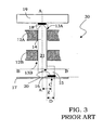
- testing head 30 shown in Figure 3 comprises an upper die 12A and a lower die 12B having respective guide holes 13A and 13B effective to house a contact probe 14.
- the contact probes 14 have contact tips 15 intended for abutting on a plurality of contact pads 16 of an integrated electronic device to be tested, schematically indicated with 17.
- the testing head 30 shown in Figure 3 comprises loose-fitting probes having a further end 18 in contact with a micro-contact strip or space transformer 19.
- a rigid arm 20 extends along a direction being perpendicular or sloping of a suitable angle with respect to the probe 14, i.e. it has an axis B-B being perpendicular or sloping with respect to an axis A-A of the contact probe 14, and it ends with the contact tip 15 of the probe 14 for the contact pads 16 of the integrated electronic device 17 to be tested.
- the contact between the tip 15 of the probe 14 and the pad 16 is spaced of a value Z with respect to the axis A-A of the contact probe 14 itself thus allowing to reduce the value of the minimum pitch of the contact tips 15 and making it possible to test integrated electronic devices with contact pads 16 with close contact centres C, i.e. reduced pitches, Z being the distance between the axis AA and a parallel axis passing through the contact centre C of the probe.
- the testing head 30 realised according to the prior art has different drawbacks.
- the method for realising the contact probe has thus to provide a deformation step which must be very precise and repeatable, in order to guarantee the fittingness of all the probes belonging to a same testing head.
- the total space of the contact probe thus realised suffers from the longitudinal size D introduced by the rigid arm 20.
- the technical problem underlying the present invention is that of devising a contact probe having a simple configuration and not needing deformation operations of the body of the probe itself, effective to ensure a good electrical contact with an integrated electronic device to be tested, and in the meantime to allow the reduction of the minimum value of the distance between adjacent probes in a testing head and thus also the pitch of the contact pads of the integrated electronic devices to be tested.
- the solution idea underlying the present invention is that of providing a testing head comprising contact probes having an eccentric contact tip positioned at one edge of the rectangular cross section of the probe body.
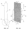
- Figure 4B shows an enlarged view of the sole end or tip 42 portion of the probe, in correspondence with a contact tip P effective to put into contact a contact pad of a device to be tested (not shown).
- the contact probe 40 has a substantially rod-like probe body 41 having axis XX and cross section of prefixed contour.
- the probe body 41 is provided in correspondence with at least one end with an eccentric contact tip P.
- the contact tip P of the probe 40 is positioned within the contour of the cross section of the probe body 41, as shown in Figure 4B where the projection P' of the contact tip P in correspondence with a section plane ⁇ has been indicated.
- “contour” of the cross section of the probe body means, in a general way, the envelope of this section defining the maximum space of the probe body, this envelope non coinciding with the geometrical perimeter of the section in the case of conformations being particular, lobed or provided with convex angles.
- the word “contour” indicates the union of the different sections, once again defining the maximum space of the probe body.
- the tip 42 portion thus defines a tip P decentralised with respect to the axis XX of the probe, but it does not increase the total space thereof.
- the contact probe 40 with eccentric contact tip P has a different space with respect to an axis YY parallel to the axis XX passing through the contact tip P.
- a plane ⁇ passing through the axis YY defines a first 40A a second 40B probe portion, these portions having different space and in particular this first portion 40A having an overall space lower than said second portion 40B.
- Figure 5 shows a preferred embodiment of the probe 40, wherein the contact tip P belongs to the contour of the cross section of the probe body.
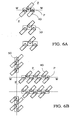
- the probe 40 has a space being totally lateral with respect to the axis YY and the probes can be close to the maximum, by alternating the arrangement in correspondence with the contact pads, as shown in the Figures 6A and 6B.
- the probes 40 have an axis ZZ of the cross section sloping with respect to an alignment axis WW of the contact pads 50.
- the contact probes 40 are arranged in an alternated way and they suitably slope, in particular according to an angle of 45°. In this way, the distance between the contact probes 40 is ensured also in correspondence with the distribution angles of the contact pads on the four sides of the integrated device to be tested, as shown in Figure 6B, where the pads have alignment axes WW and W'W' being orthogonal one another.
- the contact probes 40 advantageously have non circular section. In this way, by using corresponding guide holes with rectangular section, it is possible to orient the probes as desired in a simple and safe way.
- Figures 4A, 4B and 5 show contact probes with non circular sections, and in particular rectangular, the invention is not limited to these embodiments, traditional probes with circular sections being usable as well as probes with oval sections.
- a testing head comprising a plurality of contact probes having eccentric contact tips and thus portions of different space, suitably orientated in order to alternate these portions of different space, by reducing the minimum safety distance between the probes, thus allowing to close the corresponding contact pads on the device to be tested, i.e. reducing the pitch of this device.
- a testing head comprises at least an upper die and a lower die having respective upper and lower through-going guide holes within which at least one contact probe 40 is slidingly engaged having an eccentric contact tip P.
- the testing head comprises a plurality of contact probes 40 arranged so that probes adjacent with each other have axes ZZ sloping with respect to an alignment axis WW of the contact pads 50 of the device to be tested.
- the axes ZZ of the probes 40 and the alignment axis WW of the contact pads form an angle of 45°, as shown in the Figures 6A and 6B.
- the testing head comprises at least an air gap placed between the dies and effective to allow the contact probe 40 to deform when said contact tip P abuts on the corresponding contact pad of the device to be tested.
- the contact probes 40 have at least a pre-deformed section.
- the invention also makes reference to a method for realising a contact probe of the type comprising at least one probe body and a tip portion wherein an eccentric contact tip of the probe is defined, the method comprising at least one cutting step of the tip portion of the probe according to a plurality of cutting planes sloping with respect to the section plane ⁇ and passing through the eccentric contact tip P.
- the method for realising a contact probe according to the invention advantageously comprises the following steps:
- these cutting planes ⁇ and ⁇ slope of 45° with respect to the section plane ⁇ and they are rotated one another of 90° in order to define the eccentric contact tip P positioned inside the contour of the cross section of the probe body.
- the proposed contact probe with the eccentric tip allows to realise a testing head able to reduce the value of the minimum pitch of the contact tips P, making it thus possible to test integrated electronic devices with contact pads with very close contact centres C, i.e. very reduced pitches.
- the eccentricity of the contact tip P and the longitudinal axis A-A of the contact probe and its positioning inside the contour of the cross section of the probe body as well as a suitable orientation of the probes allow in fact to place the contact probes 40 in an alternatively opposed position with respect to the contact pads thus considerably increasing the space available for realising the guide holes and thus allowing the use of probes with greater diameters than those usable according to the prior art.
- a testing head is thus obtained being more reliable for testing the integrated electronic devices having very little pitches.
- the eccentric contact tip P is realised by means of cutting steps along cutting planes sloping with respect to the section ⁇ and passing through the contact tip P.
- the method according to the invention is extremely simplified in the case of probes having rectangular section needing only two cutting operations carried out along a first ⁇ and a second ⁇ plane sloping with respect to the section plane ⁇ and passing through the contact tip P, which belongs to the contour of the cross section of the probe body.
Landscapes
- Physics & Mathematics (AREA)
- General Physics & Mathematics (AREA)
- Geometry (AREA)
- Measuring Leads Or Probes (AREA)
- Testing Of Individual Semiconductor Devices (AREA)
- Testing Or Measuring Of Semiconductors Or The Like (AREA)
Claims (8)
- Prüfkopf mit vertikalen Prüfkontakten derart umfassend mindestens eine erste und eine zweite Matrize, die entsprechend mit mindestens einem Führungstoch zur Aufnahme mindesten eines Prüfkontakts (40) versehen sind, um den mechanischen und elektrischen Kontakt mit einem entsprechenden Kontaktfeld einer zu prüfenden integrierten elektronischen Vorrichtung sicher zu stellen, wobei mindestens ein Prüfkontakt (40) einen stangenartigen Prüfkörper (41) umfasst mit rechteckigem Querschnitt und wobei mindestens ein Ende mit einer exzentrischen Kontaktspitze (P) versehen ist, dadurch gekennzeichnet, dass die exzentrische Kontaktspitze (P) an einer Kante des rechteckigen Querschnitts angeordnet ist und erhalten wird durch Schneiden entlang einer ersten (α) und einer zweiten unterschiedlichen Schnittebene (β), die in Bezug auf eine Querschnittsebene (π) geneigt ist, die orthogonal zu einer Achse (XX) des Prüfkörpers (41) ist und durch die exzentrische Kontaktspitze (P) hindurch führt.
- Prüfkopf mit vertikalen Prüfkontakten nach Anspruch 1, dadurch gekennzeichnet, dass die Schnittebenen (α,β) sich um 45° bezüglich der Querschnittsebene (π) neigen und gegeneinander um 90° gedreht sind.
- Prüfkopf mit vertikalen Prüfkontakten nach Anspruch 1, dadurch gekennzeichnet, dass benachbarte Prüfkontakte (40) Achsen (ZZ) der rechteckigen Querschnitte der Prüfkontaktkörper (41) aufweisen, die parallel zu einer Seite der rechteckigen Querschnitte sind und sich in Bezug auf eine Ausrichtungsachse (WW) der Kontaktfelder (50) neigen.
- Prüfkopf mit vertikalen Prüfkontakten nach Anspruch 1, dadurch gekennzeichnet, dass die Achsen (ZZ) der rechteckigen Querschnitte der Prüfkontaktkörper (41) und die Ausrichtungsachse (WW) der Kontaktfelder (50) einen Winkel von 45° ausbilden.
- Prüfkopf mit vertikalen Prüfkontakten nach Anspruch 1, dadurch gekennzeichnet, dass er mindestens einen Luftspalt aufweist, der zwischen der ersten und zweiten Matrize angeordnet ist und eine Verformung des Prüfkontakts (40) ermöglicht, wenn die exzentrische Kontaktspitze (P) an ein Kontaktfeld anstößt.
- Prüfkopf mit vertikalen Prüfkontakten nach Anspruch 1, dadurch gekennzeichnet, dass der Prüfkontakt (40) mindestens einen vorverfomten Bereicht aufweist.
- Verfahren zur Herstellung eines_Prüfkontaktes der Art, der mindestens einen stangenartigen Prüfkontaktkörper (41) mit einem rechteckigen Querschnitt umfasst und in Zuordnung mit mindestens einem Spitzenbereich- mit einer exzentrischen Kontaktspitze (P) versehen ist, dadurch gekennzeichnet, dass es mindestens einen ersten und einen zweiten Schneidschritt des Spitzenbereichs entlang mindestens einer ersten Schnittebene (α) und einer zweiten unterschiedlichen Schnittebene (β) umfasst, die in Bezug auf eine Querschnittsebene (π) geneigt ist, die orthogonal zu einer Achse (XX) des Prüfkontaktkörpers (41) ausgerichtet ist, wobei die Schnittebenen durch die exzentrische Kontaktspitze (P) hindurch führen, die an einer Kante des rechteckigen Querschnitts angeordnet ist und wobei- der erste Schneidschritt entlang der ersten Schnittebene (α) durch geführt wird, die in Bezug auf die Querschnittsebene (π) geneigt ist und durch die exzentrische Kontaktspitze (P) hindurch führt, und- der zweite Schneidschritt entlang der zweiten unterschiedlichen Schnittebene (β) durchgeführt wird, die mit Bezug zu der Querschnittsebene (π) geneigt ist und durch die exzentrische Kontaktspitze (P) hindurch führt.
- Verfahren nach Anspruch 7, dadurch gekennzeichnet, dass die geneigten Ebenen (α, β) sich um 45° in Bezug auf die Querschnittsebene (π) neigen und das sie um 90° gegeneinander gedreht sind.
Priority Applications (9)
| Application Number | Priority Date | Filing Date | Title |
|---|---|---|---|
| EP04425205A EP1580562B1 (de) | 2004-03-24 | 2004-03-24 | Kontaktstift für einen Prüfkopf |
| DE602004009662T DE602004009662T2 (de) | 2004-03-24 | 2004-03-24 | Kontaktstift für einen Prüfkopf |
| AT04425205T ATE376679T1 (de) | 2004-03-24 | 2004-03-24 | Kontaktstift für einen prüfkopf |
| PL04425205T PL1580562T3 (pl) | 2004-03-24 | 2004-03-24 | Sonda kontaktowa do głowicy testującej |
| PCT/EP2005/003026 WO2005091000A1 (en) | 2004-03-24 | 2005-03-22 | Contact probe for a testing head |
| JP2007504339A JP2007530931A (ja) | 2004-03-24 | 2005-03-22 | 検査ヘッド及びコンタクトプローブの形成方法 |
| CNB2005800095316A CN100510755C (zh) | 2004-03-24 | 2005-03-22 | 用于测试头的接触探针和用于实现接触探针的方法 |
| TW094109112A TW200540427A (en) | 2004-03-24 | 2005-03-24 | Contact probe for a testing head |
| US11/090,970 US7227368B2 (en) | 2004-03-24 | 2005-03-24 | Testing head contact probe with an eccentric contact tip |
Applications Claiming Priority (1)
| Application Number | Priority Date | Filing Date | Title |
|---|---|---|---|
| EP04425205A EP1580562B1 (de) | 2004-03-24 | 2004-03-24 | Kontaktstift für einen Prüfkopf |
Publications (2)
| Publication Number | Publication Date |
|---|---|
| EP1580562A1 EP1580562A1 (de) | 2005-09-28 |
| EP1580562B1 true EP1580562B1 (de) | 2007-10-24 |
Family
ID=34854753
Family Applications (1)
| Application Number | Title | Priority Date | Filing Date |
|---|---|---|---|
| EP04425205A Expired - Lifetime EP1580562B1 (de) | 2004-03-24 | 2004-03-24 | Kontaktstift für einen Prüfkopf |
Country Status (9)
| Country | Link |
|---|---|
| US (1) | US7227368B2 (de) |
| EP (1) | EP1580562B1 (de) |
| JP (1) | JP2007530931A (de) |
| CN (1) | CN100510755C (de) |
| AT (1) | ATE376679T1 (de) |
| DE (1) | DE602004009662T2 (de) |
| PL (1) | PL1580562T3 (de) |
| TW (1) | TW200540427A (de) |
| WO (1) | WO2005091000A1 (de) |
Families Citing this family (15)
| Publication number | Priority date | Publication date | Assignee | Title |
|---|---|---|---|---|
| JP5192899B2 (ja) * | 2008-04-30 | 2013-05-08 | 東京特殊電線株式会社 | プローブ針及びその製造方法 |
| JP5372706B2 (ja) * | 2009-11-04 | 2013-12-18 | 株式会社日本マイクロニクス | プローブ針ガイド部材及びこれを備えたプローブカード並びにそれを用いる半導体装置の試験方法 |
| TWI534432B (zh) * | 2010-09-07 | 2016-05-21 | 瓊斯科技國際公司 | 用於微電路測試器之電氣傳導針腳 |
| ITMI20110615A1 (it) * | 2011-04-12 | 2012-10-13 | Technoprobe Spa | Testa di misura per un apparecchiatura di test di dispositivi elettronici |
| JP2017521668A (ja) * | 2014-07-14 | 2017-08-03 | テクノプローベ エス.ピー.エー. | 試験ヘッドのための接触プローブ、及び対応する製造方法 |
| CN107250808A (zh) * | 2014-12-04 | 2017-10-13 | 泰克诺探头公司 | 包括垂直探针的测试头 |
| TWI704352B (zh) * | 2015-03-13 | 2020-09-11 | 義大利商探針科技公司 | 測試頭之接觸探針 |
| JP2018513389A (ja) * | 2015-03-13 | 2018-05-24 | テクノプローベ エス.ピー.エー. | 様々な動作状態での試験ヘッドでのプローブ保持を適正化し、各々のガイドホールでのスライドを改善するバーチカルプローブをもつ試験ヘッド |
| JP7032167B2 (ja) * | 2018-02-09 | 2022-03-08 | 日置電機株式会社 | プローブピン、プローブユニットおよび検査装置 |
| CN108593980A (zh) * | 2018-04-18 | 2018-09-28 | 强半导体(苏州)有限公司 | 一种接触探针、测试头及接触探针的制造方法 |
| IT201800021253A1 (it) * | 2018-12-27 | 2020-06-27 | Technoprobe Spa | Testa di misura a sonde verticali avente un contatto perfezionato con un dispositivo da testare |
| KR102158735B1 (ko) * | 2019-02-15 | 2020-09-22 | 피닉슨컨트롤스 주식회사 | 플로팅 구조의 프로브 장치 |
| KR102212346B1 (ko) * | 2019-12-17 | 2021-02-04 | 주식회사 제네드 | 프로브 핀 |
| JP7816951B2 (ja) * | 2021-11-11 | 2026-02-18 | 株式会社エンプラス | コンタクトプローブ |
| CN114460338A (zh) * | 2022-01-25 | 2022-05-10 | 温州市坤顺数控科技有限公司 | 一种旋转探针接触模组 |
Family Cites Families (13)
| Publication number | Priority date | Publication date | Assignee | Title |
|---|---|---|---|---|
| EP0256541A3 (de) * | 1986-08-19 | 1990-03-14 | Feinmetall Gesellschaft mit beschrÀ¤nkter Haftung | Kontaktiervorrichtung |
| DE3818728A1 (de) * | 1988-06-01 | 1989-12-14 | Feinmetall Gmbh | Federkontaktstift |
| JPH08233860A (ja) * | 1995-02-28 | 1996-09-13 | Nec Corp | 同軸高周波プローブ及びこの同軸高周波プローブを用いた基板の評価方法 |
| US5923178A (en) * | 1997-04-17 | 1999-07-13 | Cerprobe Corporation | Probe assembly and method for switchable multi-DUT testing of integrated circuit wafers |
| US6411112B1 (en) * | 1998-02-19 | 2002-06-25 | International Business Machines Corporation | Off-axis contact tip and dense packing design for a fine pitch probe |
| TW589453B (en) * | 1998-12-02 | 2004-06-01 | Formfactor Inc | Lithographic contact elements |
| CN1231764C (zh) * | 1999-05-28 | 2005-12-14 | 日本发条株式会社 | 导电性触头 |
| JP4398061B2 (ja) * | 2000-04-28 | 2010-01-13 | 日置電機株式会社 | コンタクトプローブの製造方法 |
| ITMI20010567A1 (it) * | 2001-03-19 | 2002-09-19 | Technoprobe S R L | Testa di misura a sonde verticali per dispositivi elettronici integrati su semiconduttore |
| JP2002296297A (ja) * | 2001-03-29 | 2002-10-09 | Isao Kimoto | 接触子組立体 |
| US6906540B2 (en) * | 2001-09-20 | 2005-06-14 | Wentworth Laboratories, Inc. | Method for chemically etching photo-defined micro electrical contacts |
| US6859054B1 (en) * | 2003-08-13 | 2005-02-22 | Advantest Corp. | Probe contact system using flexible printed circuit board |
| US6967492B2 (en) * | 2003-11-26 | 2005-11-22 | Asm Assembly Automation Ltd. | Spring contact probe device for electrical testing |
-
2004
- 2004-03-24 PL PL04425205T patent/PL1580562T3/pl unknown
- 2004-03-24 EP EP04425205A patent/EP1580562B1/de not_active Expired - Lifetime
- 2004-03-24 DE DE602004009662T patent/DE602004009662T2/de not_active Expired - Lifetime
- 2004-03-24 AT AT04425205T patent/ATE376679T1/de not_active IP Right Cessation
-
2005
- 2005-03-22 CN CNB2005800095316A patent/CN100510755C/zh not_active Expired - Fee Related
- 2005-03-22 WO PCT/EP2005/003026 patent/WO2005091000A1/en not_active Ceased
- 2005-03-22 JP JP2007504339A patent/JP2007530931A/ja active Pending
- 2005-03-24 US US11/090,970 patent/US7227368B2/en not_active Expired - Lifetime
- 2005-03-24 TW TW094109112A patent/TW200540427A/zh unknown
Also Published As
| Publication number | Publication date |
|---|---|
| PL1580562T3 (pl) | 2008-02-29 |
| US7227368B2 (en) | 2007-06-05 |
| DE602004009662D1 (de) | 2007-12-06 |
| EP1580562A1 (de) | 2005-09-28 |
| US20050270044A1 (en) | 2005-12-08 |
| WO2005091000A1 (en) | 2005-09-29 |
| WO2005091000A8 (en) | 2006-01-19 |
| TW200540427A (en) | 2005-12-16 |
| CN1934453A (zh) | 2007-03-21 |
| DE602004009662T2 (de) | 2008-08-28 |
| JP2007530931A (ja) | 2007-11-01 |
| CN100510755C (zh) | 2009-07-08 |
| ATE376679T1 (de) | 2007-11-15 |
Similar Documents
| Publication | Publication Date | Title |
|---|---|---|
| EP1580562A1 (de) | Kontaktstift für einen Prüfkopf | |
| US6768327B2 (en) | Testing head having vertical probes for semiconductor integrated electronic devices | |
| US8832933B2 (en) | Method of fabricating a semiconductor test probe head | |
| CN111602063B (zh) | 悬臂接触探针及相应的探针头 | |
| US7061257B2 (en) | Probe card assembly | |
| KR100911676B1 (ko) | 콘택터, 그의 제조 방법 및 콘택터를 사용한 시험 방법 | |
| US11307222B2 (en) | Contact probe for a testing head for testing electronic devices | |
| US6144212A (en) | Vertical needle type probe card, method of manufacturing thereof, method of replacing defective probe needle and test method of wafer using the probe card | |
| US20260002964A1 (en) | Probe assembly for test and burn-in having a compliant contact element | |
| US5758537A (en) | Method and apparatus for mounting, inspecting and adjusting probe card needles | |
| US7301354B2 (en) | Contact probe for a testing head having vertical probes for semiconductor integrated devices | |
| US20200124664A1 (en) | Electrical test apparatus having adjustable contact pressure | |
| US20220043027A1 (en) | Probe module having microelectromechanical probe and method of manufacturing the same | |
| WO2021122950A1 (en) | Probe head for reduced-pitch applications | |
| EP2107380A1 (de) | Prüfkopf mit vertikalen Prüfstiften zum Verbessern des elektrischen Kontakts mit einem zu prüfenden Gerät | |
| US20200116758A1 (en) | Probe module having microelectromechanical probe and method of manufacturing the same | |
| US20120280702A1 (en) | Testing head for a test equipment of electronic devices | |
| US5867032A (en) | Process for testing a semiconductor device | |
| JPH08285890A (ja) | プローブカード | |
| EP2060922A1 (de) | Mikrostrukturprüfkopf | |
| WO2006109328A1 (en) | Contact probe for a testing head having vertical probes for semiconductor integreted electronic devices | |
| TW202232106A (zh) | 電子裝置的探針頭的接觸探針 | |
| CN121002378A (zh) | 具有改良配置的探针头 |
Legal Events
| Date | Code | Title | Description |
|---|---|---|---|
| PUAI | Public reference made under article 153(3) epc to a published international application that has entered the european phase |
Free format text: ORIGINAL CODE: 0009012 |
|
| AK | Designated contracting states |
Kind code of ref document: A1 Designated state(s): AT BE BG CH CY CZ DE DK EE ES FI FR GB GR HU IE IT LI LU MC NL PL PT RO SE SI SK TR |
|
| AX | Request for extension of the european patent |
Extension state: AL LT LV MK |
|
| 17P | Request for examination filed |
Effective date: 20060327 |
|
| AKX | Designation fees paid |
Designated state(s): AT BE BG CH CY CZ DE DK EE ES FI FR GB GR HU IE IT LI LU MC NL PL PT RO SE SI SK TR |
|
| 17Q | First examination report despatched |
Effective date: 20060710 |
|
| GRAP | Despatch of communication of intention to grant a patent |
Free format text: ORIGINAL CODE: EPIDOSNIGR1 |
|
| GRAS | Grant fee paid |
Free format text: ORIGINAL CODE: EPIDOSNIGR3 |
|
| GRAA | (expected) grant |
Free format text: ORIGINAL CODE: 0009210 |
|
| AK | Designated contracting states |
Kind code of ref document: B1 Designated state(s): AT BE BG CH CY CZ DE DK EE ES FI FR GB GR HU IE IT LI LU MC NL PL PT RO SE SI SK TR |
|
| REG | Reference to a national code |
Ref country code: GB Ref legal event code: FG4D |
|
| REG | Reference to a national code |
Ref country code: CH Ref legal event code: EP |
|
| REG | Reference to a national code |
Ref country code: IE Ref legal event code: FG4D |
|
| REF | Corresponds to: |
Ref document number: 602004009662 Country of ref document: DE Date of ref document: 20071206 Kind code of ref document: P |
|
| REG | Reference to a national code |
Ref country code: CH Ref legal event code: NV Representative=s name: ING. MARCO ZARDI C/O M. ZARDI & CO. S.A. |
|
| REG | Reference to a national code |
Ref country code: PL Ref legal event code: T3 |
|
| ET | Fr: translation filed | ||
| PG25 | Lapsed in a contracting state [announced via postgrant information from national office to epo] |
Ref country code: ES Free format text: LAPSE BECAUSE OF FAILURE TO SUBMIT A TRANSLATION OF THE DESCRIPTION OR TO PAY THE FEE WITHIN THE PRESCRIBED TIME-LIMIT Effective date: 20080204 Ref country code: SE Free format text: LAPSE BECAUSE OF FAILURE TO SUBMIT A TRANSLATION OF THE DESCRIPTION OR TO PAY THE FEE WITHIN THE PRESCRIBED TIME-LIMIT Effective date: 20080124 |
|
| PG25 | Lapsed in a contracting state [announced via postgrant information from national office to epo] |
Ref country code: BG Free format text: LAPSE BECAUSE OF FAILURE TO SUBMIT A TRANSLATION OF THE DESCRIPTION OR TO PAY THE FEE WITHIN THE PRESCRIBED TIME-LIMIT Effective date: 20080124 Ref country code: SI Free format text: LAPSE BECAUSE OF FAILURE TO SUBMIT A TRANSLATION OF THE DESCRIPTION OR TO PAY THE FEE WITHIN THE PRESCRIBED TIME-LIMIT Effective date: 20071024 Ref country code: PT Free format text: LAPSE BECAUSE OF FAILURE TO SUBMIT A TRANSLATION OF THE DESCRIPTION OR TO PAY THE FEE WITHIN THE PRESCRIBED TIME-LIMIT Effective date: 20080324 |
|
| PG25 | Lapsed in a contracting state [announced via postgrant information from national office to epo] |
Ref country code: DK Free format text: LAPSE BECAUSE OF FAILURE TO SUBMIT A TRANSLATION OF THE DESCRIPTION OR TO PAY THE FEE WITHIN THE PRESCRIBED TIME-LIMIT Effective date: 20071024 |
|
| PG25 | Lapsed in a contracting state [announced via postgrant information from national office to epo] |
Ref country code: SK Free format text: LAPSE BECAUSE OF FAILURE TO SUBMIT A TRANSLATION OF THE DESCRIPTION OR TO PAY THE FEE WITHIN THE PRESCRIBED TIME-LIMIT Effective date: 20071024 Ref country code: RO Free format text: LAPSE BECAUSE OF FAILURE TO SUBMIT A TRANSLATION OF THE DESCRIPTION OR TO PAY THE FEE WITHIN THE PRESCRIBED TIME-LIMIT Effective date: 20071024 Ref country code: BE Free format text: LAPSE BECAUSE OF FAILURE TO SUBMIT A TRANSLATION OF THE DESCRIPTION OR TO PAY THE FEE WITHIN THE PRESCRIBED TIME-LIMIT Effective date: 20071024 |
|
| PLBE | No opposition filed within time limit |
Free format text: ORIGINAL CODE: 0009261 |
|
| STAA | Information on the status of an ep patent application or granted ep patent |
Free format text: STATUS: NO OPPOSITION FILED WITHIN TIME LIMIT |
|
| 26N | No opposition filed |
Effective date: 20080725 |
|
| PG25 | Lapsed in a contracting state [announced via postgrant information from national office to epo] |
Ref country code: MC Free format text: LAPSE BECAUSE OF NON-PAYMENT OF DUE FEES Effective date: 20080331 |
|
| PG25 | Lapsed in a contracting state [announced via postgrant information from national office to epo] |
Ref country code: GR Free format text: LAPSE BECAUSE OF FAILURE TO SUBMIT A TRANSLATION OF THE DESCRIPTION OR TO PAY THE FEE WITHIN THE PRESCRIBED TIME-LIMIT Effective date: 20080125 Ref country code: EE Free format text: LAPSE BECAUSE OF FAILURE TO SUBMIT A TRANSLATION OF THE DESCRIPTION OR TO PAY THE FEE WITHIN THE PRESCRIBED TIME-LIMIT Effective date: 20071024 |
|
| PG25 | Lapsed in a contracting state [announced via postgrant information from national office to epo] |
Ref country code: FI Free format text: LAPSE BECAUSE OF FAILURE TO SUBMIT A TRANSLATION OF THE DESCRIPTION OR TO PAY THE FEE WITHIN THE PRESCRIBED TIME-LIMIT Effective date: 20071024 |
|
| PG25 | Lapsed in a contracting state [announced via postgrant information from national office to epo] |
Ref country code: CY Free format text: LAPSE BECAUSE OF FAILURE TO SUBMIT A TRANSLATION OF THE DESCRIPTION OR TO PAY THE FEE WITHIN THE PRESCRIBED TIME-LIMIT Effective date: 20071024 |
|
| PGFP | Annual fee paid to national office [announced via postgrant information from national office to epo] |
Ref country code: IE Payment date: 20090428 Year of fee payment: 6 |
|
| PGFP | Annual fee paid to national office [announced via postgrant information from national office to epo] |
Ref country code: NL Payment date: 20090427 Year of fee payment: 6 Ref country code: PL Payment date: 20090429 Year of fee payment: 6 |
|
| PGFP | Annual fee paid to national office [announced via postgrant information from national office to epo] |
Ref country code: CH Payment date: 20100324 Year of fee payment: 7 Ref country code: CZ Payment date: 20100323 Year of fee payment: 7 |
|
| PGFP | Annual fee paid to national office [announced via postgrant information from national office to epo] |
Ref country code: AT Payment date: 20100324 Year of fee payment: 7 Ref country code: GB Payment date: 20100329 Year of fee payment: 7 |
|
| PG25 | Lapsed in a contracting state [announced via postgrant information from national office to epo] |
Ref country code: HU Free format text: LAPSE BECAUSE OF FAILURE TO SUBMIT A TRANSLATION OF THE DESCRIPTION OR TO PAY THE FEE WITHIN THE PRESCRIBED TIME-LIMIT Effective date: 20080425 Ref country code: LU Free format text: LAPSE BECAUSE OF NON-PAYMENT OF DUE FEES Effective date: 20080324 |
|
| PG25 | Lapsed in a contracting state [announced via postgrant information from national office to epo] |
Ref country code: TR Free format text: LAPSE BECAUSE OF FAILURE TO SUBMIT A TRANSLATION OF THE DESCRIPTION OR TO PAY THE FEE WITHIN THE PRESCRIBED TIME-LIMIT Effective date: 20071024 |
|
| PGFP | Annual fee paid to national office [announced via postgrant information from national office to epo] |
Ref country code: IT Payment date: 20100329 Year of fee payment: 7 |
|
| REG | Reference to a national code |
Ref country code: NL Ref legal event code: V1 Effective date: 20101001 |
|
| PG25 | Lapsed in a contracting state [announced via postgrant information from national office to epo] |
Ref country code: IE Free format text: LAPSE BECAUSE OF NON-PAYMENT OF DUE FEES Effective date: 20100324 Ref country code: NL Free format text: LAPSE BECAUSE OF NON-PAYMENT OF DUE FEES Effective date: 20101001 |
|
| REG | Reference to a national code |
Ref country code: CH Ref legal event code: PL |
|
| GBPC | Gb: european patent ceased through non-payment of renewal fee |
Effective date: 20110324 |
|
| PG25 | Lapsed in a contracting state [announced via postgrant information from national office to epo] |
Ref country code: CZ Free format text: LAPSE BECAUSE OF NON-PAYMENT OF DUE FEES Effective date: 20110324 Ref country code: AT Free format text: LAPSE BECAUSE OF NON-PAYMENT OF DUE FEES Effective date: 20110324 |
|
| REG | Reference to a national code |
Ref country code: PL Ref legal event code: LAPE |
|
| PG25 | Lapsed in a contracting state [announced via postgrant information from national office to epo] |
Ref country code: LI Free format text: LAPSE BECAUSE OF NON-PAYMENT OF DUE FEES Effective date: 20110331 Ref country code: CH Free format text: LAPSE BECAUSE OF NON-PAYMENT OF DUE FEES Effective date: 20110331 |
|
| PG25 | Lapsed in a contracting state [announced via postgrant information from national office to epo] |
Ref country code: GB Free format text: LAPSE BECAUSE OF NON-PAYMENT OF DUE FEES Effective date: 20110324 Ref country code: PL Free format text: LAPSE BECAUSE OF NON-PAYMENT OF DUE FEES Effective date: 20100324 Ref country code: IT Free format text: LAPSE BECAUSE OF NON-PAYMENT OF DUE FEES Effective date: 20110324 |
|
| PGFP | Annual fee paid to national office [announced via postgrant information from national office to epo] |
Ref country code: FR Payment date: 20120403 Year of fee payment: 9 |
|
| REG | Reference to a national code |
Ref country code: FR Ref legal event code: ST Effective date: 20131129 |
|
| PG25 | Lapsed in a contracting state [announced via postgrant information from national office to epo] |
Ref country code: FR Free format text: LAPSE BECAUSE OF NON-PAYMENT OF DUE FEES Effective date: 20130402 |
|
| PGFP | Annual fee paid to national office [announced via postgrant information from national office to epo] |
Ref country code: DE Payment date: 20210223 Year of fee payment: 18 |
|
| REG | Reference to a national code |
Ref country code: DE Ref legal event code: R119 Ref document number: 602004009662 Country of ref document: DE |
|
| PG25 | Lapsed in a contracting state [announced via postgrant information from national office to epo] |
Ref country code: DE Free format text: LAPSE BECAUSE OF NON-PAYMENT OF DUE FEES Effective date: 20221001 |