EP1581968B1 - Integrierte anitfuse-struktur für finfet- und cmos-vorrichtungen - Google Patents
Integrierte anitfuse-struktur für finfet- und cmos-vorrichtungen Download PDFInfo
- Publication number
- EP1581968B1 EP1581968B1 EP02808339A EP02808339A EP1581968B1 EP 1581968 B1 EP1581968 B1 EP 1581968B1 EP 02808339 A EP02808339 A EP 02808339A EP 02808339 A EP02808339 A EP 02808339A EP 1581968 B1 EP1581968 B1 EP 1581968B1
- Authority
- EP
- European Patent Office
- Prior art keywords
- corners
- layer
- semiconducting material
- oxide
- oxide layer
- Prior art date
- Legal status (The legal status is an assumption and is not a legal conclusion. Google has not performed a legal analysis and makes no representation as to the accuracy of the status listed.)
- Expired - Lifetime
Links
Images




Classifications
-
- H—ELECTRICITY
- H10—SEMICONDUCTOR DEVICES; ELECTRIC SOLID-STATE DEVICES NOT OTHERWISE PROVIDED FOR
- H10D—INORGANIC ELECTRIC SEMICONDUCTOR DEVICES
- H10D86/00—Integrated devices formed in or on insulating or conducting substrates, e.g. formed in silicon-on-insulator [SOI] substrates or on stainless steel or glass substrates
- H10D86/01—Manufacture or treatment
-
- H—ELECTRICITY
- H10—SEMICONDUCTOR DEVICES; ELECTRIC SOLID-STATE DEVICES NOT OTHERWISE PROVIDED FOR
- H10D—INORGANIC ELECTRIC SEMICONDUCTOR DEVICES
- H10D84/00—Integrated devices formed in or on semiconductor substrates that comprise only semiconducting layers, e.g. on Si wafers or on GaAs-on-Si wafers
- H10D84/80—Integrated devices formed in or on semiconductor substrates that comprise only semiconducting layers, e.g. on Si wafers or on GaAs-on-Si wafers characterised by the integration of at least one component covered by groups H10D12/00 or H10D30/00, e.g. integration of IGFETs
- H10D84/811—Combinations of field-effect devices and one or more diodes, capacitors or resistors
-
- H—ELECTRICITY
- H10—SEMICONDUCTOR DEVICES; ELECTRIC SOLID-STATE DEVICES NOT OTHERWISE PROVIDED FOR
- H10D—INORGANIC ELECTRIC SEMICONDUCTOR DEVICES
- H10D84/00—Integrated devices formed in or on semiconductor substrates that comprise only semiconducting layers, e.g. on Si wafers or on GaAs-on-Si wafers
- H10D84/90—Masterslice integrated circuits
- H10D84/903—Masterslice integrated circuits comprising field effect technology
- H10D84/907—CMOS gate arrays
-
- H—ELECTRICITY
- H10—SEMICONDUCTOR DEVICES; ELECTRIC SOLID-STATE DEVICES NOT OTHERWISE PROVIDED FOR
- H10D—INORGANIC ELECTRIC SEMICONDUCTOR DEVICES
- H10D86/00—Integrated devices formed in or on insulating or conducting substrates, e.g. formed in silicon-on-insulator [SOI] substrates or on stainless steel or glass substrates
- H10D86/201—Integrated devices formed in or on insulating or conducting substrates, e.g. formed in silicon-on-insulator [SOI] substrates or on stainless steel or glass substrates the substrates comprising an insulating layer on a semiconductor body, e.g. SOI
-
- H—ELECTRICITY
- H10—SEMICONDUCTOR DEVICES; ELECTRIC SOLID-STATE DEVICES NOT OTHERWISE PROVIDED FOR
- H10W—GENERIC PACKAGES, INTERCONNECTIONS, CONNECTORS OR OTHER CONSTRUCTIONAL DETAILS OF DEVICES COVERED BY CLASS H10
- H10W20/00—Interconnections in chips, wafers or substrates
- H10W20/40—Interconnections external to wafers or substrates, e.g. back-end-of-line [BEOL] metallisations or vias connecting to gate electrodes
- H10W20/49—Adaptable interconnections, e.g. fuses or antifuses
- H10W20/491—Antifuses, i.e. interconnections changeable from non-conductive to conductive
-
- H—ELECTRICITY
- H10—SEMICONDUCTOR DEVICES; ELECTRIC SOLID-STATE DEVICES NOT OTHERWISE PROVIDED FOR
- H10D—INORGANIC ELECTRIC SEMICONDUCTOR DEVICES
- H10D30/00—Field-effect transistors [FET]
- H10D30/60—Insulated-gate field-effect transistors [IGFET]
- H10D30/62—Fin field-effect transistors [FinFET]
-
- H—ELECTRICITY
- H10—SEMICONDUCTOR DEVICES; ELECTRIC SOLID-STATE DEVICES NOT OTHERWISE PROVIDED FOR
- H10D—INORGANIC ELECTRIC SEMICONDUCTOR DEVICES
- H10D30/00—Field-effect transistors [FET]
- H10D30/60—Insulated-gate field-effect transistors [IGFET]
- H10D30/62—Fin field-effect transistors [FinFET]
- H10D30/6212—Fin field-effect transistors [FinFET] having fin-shaped semiconductor bodies having non-rectangular cross-sections
- H10D30/6213—Fin field-effect transistors [FinFET] having fin-shaped semiconductor bodies having non-rectangular cross-sections having rounded corners
Definitions
- This invention relates to the manufacture of very large-scale integrated devices, particularly FINFET and planar CMOS devices, with electrical antifuses integrated therein.
- FETs field-effect transistors
- FIG. 1A shows two such fin structures 1, 2 formed on a silicon-on-insulator (SOI) substrate, where the top of the bulk silicon substrate 10 has a buried oxide (BOX) layer 3 formed thereon, and the devices are made in a further silicon layer overlying the BOX.
- SOI silicon-on-insulator
- BOX buried oxide
- Silicon fins 11,21 are shown after being formed by etching of this silicon layer down to the BOX surface, using an etching hardmask 12,22 for image transfer.
- a gate oxide may then be grown on both faces of a silicon fin (such as faces 1 la and 1 Ib of fin 11).
- the FINFET technology shows promise in offering higher areal gate density than more conventional planar CMOS devices, as well as better device performance, and lower power consumption.
- fuses are conductors which may easily be removed (“blown") to create open circuits
- antifuses are areas of dielectric which may be electrically broken down to form a permanent conducting path.
- Fuses and antifuses are preferably formed with minimal expense of chip area and require no additional lithographic steps. Recent scaling of fuses has not kept up with the scaling rate of the rest of the silicon features, so that chip regions devoted to fuses are occupying a larger percentage of the total chip area.
- etching of the isolation trench may create sharp corners in the silicon where the sidewall of the trench meets the top silicon surface or the trench bottom. If these corners are not rounded by further processing, a dielectric layer overlying the corners may be thinned and present reliability problems (see U.S. Pat. No. 6,150,234 ). Similarly, etching of a contact hole through a dielectric layer may result in a trench with sharp corners.
- STI shallow-trench isolation
- a sharp trench corner presents an opportunity to conveniently form antifuses (the trench being etched in a conductive material or being coated with a conductive material), since the electric field is generally enhanced at the comer; while an insulating layer overlying the corner is thinned (see U.S. Pat. No. 5,502,000 ; U.S. Pat No. 5,322,812 , U.S. Pat. No. 6,096,580 and references cited therein; and Chen et al., IEEE Electron Device Letters 13, 53 (1992 )). Examples of conventional antifuse structures are described in US 5,915,171 and US2001/015472 .
- electrical fuses rather than mechanical fuses as part of the transistor fabrication process.
- Conventional fuses are "blown” via laser ablation or other mechanical means to create an electrical open.
- Electrical fuses or antifuses are "blown” via internal electrical wiring in the chip; the area requirement for electrical fuses/antifuses is therefore much less.
- mechanical fuses require a protection region around and below them, to prevent the fuse-blowing technique from having other detrimental impacts on the chip circuits. Electrical fuses and antifuses do not have this requirement. To save chip area and thus reduce manufacturing cost, it therefore is desirable to fabricate electrical fuses or antifuses which may be integrated with fabrication of FINFET and planar CMOS devices, with a minimum number of additional fabrication steps.
- a method for fabricating an antifuse structure integrated with a semiconductor device comprising the steps of: forming a region of semiconducting material overlying an insulator disposed on a substrate; performing an etching process to expose a plurality of corners in the semiconducting material; forming a plurality of elongated tips of the semiconducting material at the respective corners by oxidizing the exposed corners to form an oxide film, with internal stresses in the oxide film thus produced at the corners being oriented to reduce oxygen diffusion rate at the corners thereby producing the tips; removing the oxide film; subsequently forming an oxide layer on the semiconducting material and overlying the corners, the oxide layer having a nominal thickness and a reduced thickness at the corners less than the nominal thickness; and forming a layer of conducting material in contact with the oxide layer at the corners, thereby forming a plurality of possible breakdown paths at said corners, between the semiconducting material and the layer of conducting material through the oxide layer.
- a preferred embodiment of the present invention addresses the above-described need by providing a method for fabricating an antifuse structure integrated with a semiconductor device, with a minimum of additional process steps.
- a region of semiconducting material is provided overlying an insulator disposed on a substrate; an etching process exposes a plurality of corners in the semiconducting material.
- the exposed corners are oxidized to form elongated tips at the comers; the oxide overlying the tips is removed.
- An oxide layer, such as a gate oxide, is then formed on the semiconducting material and overlying the comers; this layer has a reduced thickness at the corners.
- a layer of conducting material is formed in contact with the oxide layer at the corners, thereby forming a plurality of possible breakdown paths between the semiconducting material and the layer of conducting material through the oxide layer.
- Applying a voltage, such as a bum-in voltage, to the structure converts at least one of the breakdown paths to a conducting path, when it is desired to activate a specific antifuse electrically.
- This process may be practised with FINFET or planar CMOS devices, so that the antifuse structures are integrated with those devices.
- the antifuse structures fabricated with this process each have a plurality of possible breakdown paths which are electrically in parallel.
- a conducting path may be formed by breaking down the oxide layer at any of these paths. This redundancy helps to ensure that the device will be programmable.
- the applied voltage is typically about 1.5 times the nominal voltage for the device.
- an antifuse structure which is integrated with a semiconductor device.
- the antifuse structure includes a region of semiconducting material overlying an insulator disposed on a substrate; the semiconducting material has a plurality of corners with a plurality of elongated tips of the semiconducting material at the respective corners.
- An oxide layer is disposed on the semiconducting material and overlying the comers; the oxide layer has a nominal thickness and a reduced thickness at the corners less than the nominal thickness.
- the structure also includes a layer of conducting material in contact with the oxide layer at the corners. A feature of the structure is that a plurality of possible breakdown paths are disposed at the corners, between the semiconducting material and the layer of conducting material through the reduced thickness of the oxide layer.
- antifuse structures are integrated at the silicon level, and accordingly require minimal chip area.
- the fabrication.process for the antifuses requires only one additional masking layer, relative to the standard transistor fabrication processes.
- a plurality of antifuses is formed at a semiconducting gate structure by oxidation of exposed corners. This process may be applied to either FINFET or planar CMOS gate structures, as detailed below.
- FIG 1A shows two neighboring silicon fms 11,21 which may form the bodies of FINFETs after gate electrode processing.
- one of these (fin 11) is instead made into an antifuse structure.
- the fin structure 2, which includes fin 21 and hardmask 22, is coated with a protective layer of resist 25; the resist is exposed and developed to uncover fin structure 1.
- the exposed portion of the BOX layer 3 is then subjected to an isotropic etch which undercuts silicon fin 11 (see Figure IB).
- the hardmask 12 is also removed in this step. It should be noted that the etching and undercutting results in four exposed corners 111-114 on silicon fin 11.
- the silicon surface of fin 11 is then oxidized in a low-temperature oxidation process, to form an oxide layer 31 thereon.
- the oxidation process is preferably a dry/wet/dry process at 900 °C. which is known to those skilled in the art.
- two-dimensional stresses at the corners 111-114 result in formation of elongated tips of silicon lilt, 112t, 113t, 114t, shown on an exaggerated scale in Figure 1C . These tips are created during oxidation as the stress in the oxide film at the corners reduces the oxygen diffusion rate.
- Oxide layer 31 is then removed in an isotropic etch process, after which resist 25 is stripped (see Figure ID).
- n+ ion implantation may be advantageously performed into the fuse region before resist 25 is removed. Although not required for operability of the structure as an antifuse, this implantation process makes the silicon portion of the fuse an improved conductor, and improves the performance of the fin in terms of required programming voltage and reliability.
- a standard gate oxide preclean is then performed on both silicon fins 11 and 21, after which a gate oxide 51, 52 is grown on the exposed surfaces of fins 11 and 21 respectively.
- the thickness of the gate oxide is typically in the range 15-40 A.
- a polysilicon conductor layer 60 is then deposited over the fins; this polysilicon layer serves as the gate conductor for the FINFET 200, while providing a conducting path in the antifuse 100.
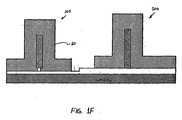
- a resist layer 65 is deposited over both structures and patterned to define the transistor gates, as well as one node of the fuse. As shown in Figure IE, opening 66 separates the two types of structures. The portion of polysilicon layer 60 exposed in this opening is then etched, and resist 65 is stripped away. The FINFET structure 200 and the antifuse structure 100 are thus electrically isolated from each other (see Figure IF) .
- Figure 1G is a detail view showing the gate oxide 51 overlying the corners of fin 11 having tips 11 It, 112t, 113t, 114t, with a reduced thickness at the corners (tips) relative to the nominal thickness thereof.
- the tips at the corners are shown in an exaggerated fashion for the purposes of illustration; actual thinning of the oxide is approximately 15%-30% as compared with the oxide covering the central area on the face of the fin.
- the tips in Figure IG are shown only in cross-section; it should be understood that an elongated tip is formed along the edge of the fin, so that sharp ridges run the length of the fin, normal to the plane of the figure.
- a programming or writing operation for the antifuse (that is, converting the antifuse into a conducting path) thus comprises applying a voltage sufficient to cause breakdown at one of the corners (such as corner 113 in Figure 1G , creating breakdown path 103). It has been found that the writing operation can be performed effectively using the bum-in voltage for the FET devices, which is typically 1.5 times the nominal voltage.
- the bum-in voltage would be about 1.8 V. Accordingly, a writing operation on the antifuse may be performed at bum-in voltages without adversely affecting the normal operation of the other devices on the chip.
- FIG. 2A shows three silicon gate regions 211,212,213, where region 211 is to be made into an antifuse instead of a FET.
- the silicon regions are disposed on a buried oxide (BOX) 203 on substrate 210, and are separated by shallow trench isolation regions (STI) 215.
- a resist layer 205 is deposited over all the silicon regions, and then patterned so that an opening 220 in the resist exposes silicon region 211 and portions of isolation regions 215 which are to be fabricated into an antifuse.
- the STI material 215 typically oxide
- a low-temperature oxidation process is then performed so that the exposed silicon surface is covered by an oxide layer 231, as shown in Figure 2B .
- This oxidation process causes formation of silicon tips 21 It at the corners, as shown in Figure 2C .
- the tips are shown only in cross section; sharp ridges run the length of region 211 normal to the plane of the figure.
- the oxide layer 231 is then removed using an isotropic etch process. At this point it is preferred, but not required, that silicon region 211 (which will become the antifuse) be implanted with an n+ dopant, in order to facilitate programming (writing) of the antifuse. Resist 205 is then removed.
- a standard preclean is then performed and a gate oxide 251, 252, 253 is grown on the surface of silicon regions 211, 232,213 respectively (see Figure 2D ).
- This gate oxide is typically 10-20 A thick.
- a polysilicon layer 260 is deposited on all the silicon and isolation regions. This layer is then patterned with the transistor gate images, as well as defining one node of the antifuse, and etched so that openings 266 are formed over the isolation regions 215, electrically isolating the MOS device regions from the antifuse and from each other.
- Figure 2E is a detail view of the antifuse structure for planar CMOS devices.
- the thinning of the gate oxide near the tips 21 It is exaggerated for purposes of illustration; the gate oxide at this location is typically 15% to 30% thinner than at the central area of the antifuse (that is, layer 251 has a reduced thickness at the corners 15% to 30% less than the nominal thickness of 10-20 A). Since at least two exposed corners of the silicon have been oxidized, there are at least two potential breakdown paths between the doped silicon region 211 and the polysilicon conductor 260. Programming (writing) the antifuse using a voltage as low as the burn-in voltage creates conducting path 280, shown schematically in Figure 2E .
- the present invention is generally applicable to the problem of fabricating field-programmable gate arrays which are often required for application-specific integrated circuits (ASICs).
- ASICs application-specific integrated circuits
- antifuses can be used to re-route data for redundancy, such as in memory circuits, or in advanced microprocessors.
- the invention is applicable to gate arrays or SRAMs employing FINFET or planar CMOS technology.
- An important advantage of the invention is that redundant breakdown points are provided at each antifuse location.
- the antifuse fabrication process requires only one additional masking layer relative to the standard transistor fabrication process.
- the antifuses are fabricated at the silicon level (that is, during the process of building the neighboring transistors), resulting in significant saving of area on the chip.
Landscapes
- Design And Manufacture Of Integrated Circuits (AREA)
- Semiconductor Memories (AREA)
- Metal-Oxide And Bipolar Metal-Oxide Semiconductor Integrated Circuits (AREA)
- Thin Film Transistor (AREA)
- Formation Of Insulating Films (AREA)
Claims (5)
- Verfahren zur Herstellung einer Antifuse-Struktur (100), die mit einer Halbleitervorrichtung integriert ausgebildet ist, wobei das Verfahren die folgenden Schritte umfasst:Bilden eines Bereichs eines Halbleitermaterials (11), welches einen Isolator (3) überlagert, der auf einem Substrat (10) angeordnet ist;Durchführen eines Ätzverfahrens, um mehrere Ecken (111 bis 114) in dem Halbleitermaterial frei zu legen;Bilden mehrerer länglicher Spitzen (111t, 112t, 113t, 114t) des Halbleitermaterials an den entsprechenden Ecken durch Oxidieren der frei liegenden Ecken (111, 112, 113, 114), um eine Oxid-Dünnschicht (31) zu bilden, wobei innere Spannungen in der so erzeugten Oxid-Dünnschicht an den Ecken die Sauerstoff-Diffusionsgeschwindigkeit an den Ecken verringern, wodurch die Spitzen erzeugt werden;Entfernen der Oxid-Dünnschicht (31);anschließendes Bilden einer Oxidschicht (51) auf dem Halbleitermaterial, welche die Ecken überlagert, wobei die Oxidschicht eine Nenndicke aufweist und an den Ecken eine reduzierte Dicke aufweist, die geringer als die Nenndicke ist; undBilden einer Schicht eines leitenden Materials (60) in Kontakt mit der Oxidschicht (51) an den Ecken, wodurch an den Ecken mehrere mögliche Durchschlagspfade zwischen dem Halbleitermaterial und der Schicht des leitenden Materials durch die Oxidschicht hindurch gebildet werden.
- Verfahren nach Anspruch 1, dadurch gekennzeichnet, dass der Oxidationsschritt über ein Tieftemperatur-Oxidationsverfahren durchgeführt wird.
- Verfahren nach einem der vorhergehenden Ansprüche, welches ferner den Schritt des Anlegens einer Spannung an die Antifuse-Struktur umfasst, wodurch mindestens einer der Durchschlagspfade zu einem Leitweg (103, 280) durch die Oxidschicht (51, 251) hindurch umgewandelt wird.
- Verfahren nach Anspruch 3, dadurch gekennzeichnet, dass die Spannung gemäß einem Einbrennverfahren für die Vorrichtung angelegt wird.
- Verfahren nach Anspruch 3, dadurch gekennzeichnet, dass die Vorrichtung eine Nennspannung aufweist und die angelegte Spannung das 1,5-fache der Nennspannung beträgt.
Applications Claiming Priority (1)
| Application Number | Priority Date | Filing Date | Title |
|---|---|---|---|
| PCT/US2002/041182 WO2004059726A1 (en) | 2002-12-20 | 2002-12-20 | Integrated antifuse structure for finfet and cmos devices |
Publications (3)
| Publication Number | Publication Date |
|---|---|
| EP1581968A1 EP1581968A1 (de) | 2005-10-05 |
| EP1581968A4 EP1581968A4 (de) | 2007-04-18 |
| EP1581968B1 true EP1581968B1 (de) | 2010-05-12 |
Family
ID=32679942
Family Applications (1)
| Application Number | Title | Priority Date | Filing Date |
|---|---|---|---|
| EP02808339A Expired - Lifetime EP1581968B1 (de) | 2002-12-20 | 2002-12-20 | Integrierte anitfuse-struktur für finfet- und cmos-vorrichtungen |
Country Status (7)
| Country | Link |
|---|---|
| EP (1) | EP1581968B1 (de) |
| JP (1) | JP4418760B2 (de) |
| CN (1) | CN1314124C (de) |
| AT (1) | ATE467905T1 (de) |
| AU (1) | AU2002368525A1 (de) |
| DE (1) | DE60236375D1 (de) |
| WO (1) | WO2004059726A1 (de) |
Families Citing this family (30)
| Publication number | Priority date | Publication date | Assignee | Title |
|---|---|---|---|---|
| US7358121B2 (en) | 2002-08-23 | 2008-04-15 | Intel Corporation | Tri-gate devices and methods of fabrication |
| US6909151B2 (en) | 2003-06-27 | 2005-06-21 | Intel Corporation | Nonplanar device with stress incorporation layer and method of fabrication |
| US7456476B2 (en) | 2003-06-27 | 2008-11-25 | Intel Corporation | Nonplanar semiconductor device with partially or fully wrapped around gate electrode and methods of fabrication |
| US7105390B2 (en) | 2003-12-30 | 2006-09-12 | Intel Corporation | Nonplanar transistors with metal gate electrodes |
| US7624192B2 (en) | 2003-12-30 | 2009-11-24 | Microsoft Corporation | Framework for user interaction with multiple network devices |
| US7268058B2 (en) | 2004-01-16 | 2007-09-11 | Intel Corporation | Tri-gate transistors and methods to fabricate same |
| US7154118B2 (en) | 2004-03-31 | 2006-12-26 | Intel Corporation | Bulk non-planar transistor having strained enhanced mobility and methods of fabrication |
| US7579280B2 (en) | 2004-06-01 | 2009-08-25 | Intel Corporation | Method of patterning a film |
| US7042009B2 (en) | 2004-06-30 | 2006-05-09 | Intel Corporation | High mobility tri-gate devices and methods of fabrication |
| US7422946B2 (en) * | 2004-09-29 | 2008-09-09 | Intel Corporation | Independently accessed double-gate and tri-gate transistors in same process flow |
| US7332439B2 (en) | 2004-09-29 | 2008-02-19 | Intel Corporation | Metal gate transistors with epitaxial source and drain regions |
| US7361958B2 (en) | 2004-09-30 | 2008-04-22 | Intel Corporation | Nonplanar transistors with metal gate electrodes |
| US20060086977A1 (en) | 2004-10-25 | 2006-04-27 | Uday Shah | Nonplanar device with thinned lower body portion and method of fabrication |
| US7193279B2 (en) | 2005-01-18 | 2007-03-20 | Intel Corporation | Non-planar MOS structure with a strained channel region |
| US7518196B2 (en) | 2005-02-23 | 2009-04-14 | Intel Corporation | Field effect transistor with narrow bandgap source and drain regions and method of fabrication |
| US20060202266A1 (en) | 2005-03-14 | 2006-09-14 | Marko Radosavljevic | Field effect transistor with metal source/drain regions |
| US7858481B2 (en) | 2005-06-15 | 2010-12-28 | Intel Corporation | Method for fabricating transistor with thinned channel |
| US7547637B2 (en) | 2005-06-21 | 2009-06-16 | Intel Corporation | Methods for patterning a semiconductor film |
| US7279375B2 (en) | 2005-06-30 | 2007-10-09 | Intel Corporation | Block contact architectures for nanoscale channel transistors |
| US7402875B2 (en) | 2005-08-17 | 2008-07-22 | Intel Corporation | Lateral undercut of metal gate in SOI device |
| US7479421B2 (en) | 2005-09-28 | 2009-01-20 | Intel Corporation | Process for integrating planar and non-planar CMOS transistors on a bulk substrate and article made thereby |
| US20070090416A1 (en) | 2005-09-28 | 2007-04-26 | Doyle Brian S | CMOS devices with a single work function gate electrode and method of fabrication |
| US7485503B2 (en) | 2005-11-30 | 2009-02-03 | Intel Corporation | Dielectric interface for group III-V semiconductor device |
| US8143646B2 (en) | 2006-08-02 | 2012-03-27 | Intel Corporation | Stacking fault and twin blocking barrier for integrating III-V on Si |
| US8362566B2 (en) | 2008-06-23 | 2013-01-29 | Intel Corporation | Stress in trigate devices using complimentary gate fill materials |
| US8030736B2 (en) * | 2009-08-10 | 2011-10-04 | International Business Machines Corporation | Fin anti-fuse with reduced programming voltage |
| DE112011105751B4 (de) | 2011-10-18 | 2024-05-08 | Intel Corporation | Antifuse-Element unter Verwendung von nicht-planarer Topologie |
| US9536883B2 (en) * | 2012-07-12 | 2017-01-03 | Broadcom Corporation | Dual anti-fuse |
| CN103730367B (zh) * | 2012-10-16 | 2017-05-03 | 中国科学院微电子研究所 | 半导体器件制造方法 |
| US11515251B2 (en) * | 2018-04-02 | 2022-11-29 | Intel Corporation | FinFET transistors as antifuse elements |
Family Cites Families (10)
| Publication number | Priority date | Publication date | Assignee | Title |
|---|---|---|---|---|
| US5322812A (en) | 1991-03-20 | 1994-06-21 | Crosspoint Solutions, Inc. | Improved method of fabricating antifuses in an integrated circuit device and resulting structure |
| US5557136A (en) * | 1991-04-26 | 1996-09-17 | Quicklogic Corporation | Programmable interconnect structures and programmable integrated circuits |
| US5475253A (en) | 1992-08-21 | 1995-12-12 | Xilinx, Inc. | Antifuse structure with increased breakdown at edges |
| US5572062A (en) * | 1994-03-31 | 1996-11-05 | Crosspoint Solutions, Inc. | Antifuse with silicon spacers |
| TW347587B (en) * | 1997-10-20 | 1998-12-11 | United Semiconductor Corp | Antifuse structure and process for producing the same |
| US6130469A (en) * | 1998-04-24 | 2000-10-10 | International Business Machines Corporation | Electrically alterable antifuse using FET |
| US6096580A (en) | 1999-09-24 | 2000-08-01 | International Business Machines Corporation | Low programming voltage anti-fuse |
| US6150234A (en) | 1999-12-16 | 2000-11-21 | Vlsi Technology, Inc. | Trench-diffusion corner rounding in a shallow-trench (STI) process |
| US6774439B2 (en) | 2000-02-17 | 2004-08-10 | Kabushiki Kaisha Toshiba | Semiconductor device using fuse/anti-fuse system |
| US6413802B1 (en) * | 2000-10-23 | 2002-07-02 | The Regents Of The University Of California | Finfet transistor structures having a double gate channel extending vertically from a substrate and methods of manufacture |
-
2002
- 2002-12-20 AT AT02808339T patent/ATE467905T1/de not_active IP Right Cessation
- 2002-12-20 AU AU2002368525A patent/AU2002368525A1/en not_active Abandoned
- 2002-12-20 EP EP02808339A patent/EP1581968B1/de not_active Expired - Lifetime
- 2002-12-20 JP JP2004563149A patent/JP4418760B2/ja not_active Expired - Fee Related
- 2002-12-20 WO PCT/US2002/041182 patent/WO2004059726A1/en not_active Ceased
- 2002-12-20 CN CNB028300467A patent/CN1314124C/zh not_active Expired - Fee Related
- 2002-12-20 DE DE60236375T patent/DE60236375D1/de not_active Expired - Lifetime
Also Published As
| Publication number | Publication date |
|---|---|
| DE60236375D1 (de) | 2010-06-24 |
| EP1581968A1 (de) | 2005-10-05 |
| CN1714439A (zh) | 2005-12-28 |
| AU2002368525A1 (en) | 2004-07-22 |
| JP4418760B2 (ja) | 2010-02-24 |
| CN1314124C (zh) | 2007-05-02 |
| ATE467905T1 (de) | 2010-05-15 |
| JP2006511093A (ja) | 2006-03-30 |
| WO2004059726A1 (en) | 2004-07-15 |
| EP1581968A4 (de) | 2007-04-18 |
Similar Documents
| Publication | Publication Date | Title |
|---|---|---|
| US7087499B2 (en) | Integrated antifuse structure for FINFET and CMOS devices | |
| EP1581968B1 (de) | Integrierte anitfuse-struktur für finfet- und cmos-vorrichtungen | |
| JP4006419B2 (ja) | ハイブリッド・プレーナおよびFinFETCMOSデバイス | |
| EP1620891B1 (de) | Methode zur herstellung von finfets mit mehreren höhen | |
| US7338840B1 (en) | Method of forming a semiconductor die with heat and electrical pipes | |
| US7696565B2 (en) | FinFET body contact structure | |
| US5057451A (en) | Method of forming an antifuse element with substantially reduced capacitance using the locos technique | |
| TWI503979B (zh) | 包含一場效電晶體於一覆矽的絕緣層構造的半導體裝置 | |
| JP4233953B2 (ja) | 垂直型動的ランダム・アクセス・メモリ(dram)・アレイと論理回路部を含む複合型集積回路を作製する方法 | |
| JP2004088101A (ja) | 集積回路チップおよびその製造方法 | |
| US6261937B1 (en) | Method for forming a semiconductor fuse | |
| JP2743061B2 (ja) | 少なくとも2つの導電性エレメントを含む集積回路内の構造およびその製造の方法 | |
| EP1586108B1 (de) | Finfet sram-zelle mit invertierten finfet-dünnschichttransistoren | |
| JP2002314094A (ja) | 高性能論理のために、soiプロセスと共に使用可能な高密度埋め込みコンタクトを生成する方法及び構造 | |
| US8530319B2 (en) | Vertical silicide e-fuse | |
| JP3273001B2 (ja) | 半導体記憶装置とその製造方法 | |
| CN113611703B (zh) | 制造半导体结构的方法 | |
| JP3340177B2 (ja) | 電界効果型トランジスタ | |
| KR100781615B1 (ko) | Finfet 및 cmos 디바이스들을 위한 집적안티퓨즈 구조 | |
| JP2538856B2 (ja) | 半導体装置の製造方法 | |
| EP2599111B1 (de) | Transistor mit gegenelektrodenanschluss mit dem source/drain-kontakt | |
| CN114864584A (zh) | 存储器装置及其制造方法 | |
| JP3795798B2 (ja) | 半導体記憶装置 | |
| JP3295393B2 (ja) | 半導体装置の製造方法 | |
| US11355401B1 (en) | Field effect transistor |
Legal Events
| Date | Code | Title | Description |
|---|---|---|---|
| PUAI | Public reference made under article 153(3) epc to a published international application that has entered the european phase |
Free format text: ORIGINAL CODE: 0009012 |
|
| 17P | Request for examination filed |
Effective date: 20050622 |
|
| AK | Designated contracting states |
Kind code of ref document: A1 Designated state(s): AT BE BG CH CY CZ DE DK EE ES FI FR GB GR IE IT LI LU MC NL PT SE SI SK TR |
|
| AX | Request for extension of the european patent |
Extension state: AL LT LV MK RO |
|
| DAX | Request for extension of the european patent (deleted) | ||
| A4 | Supplementary search report drawn up and despatched |
Effective date: 20070321 |
|
| RIC1 | Information provided on ipc code assigned before grant |
Ipc: H01L 23/525 20060101AFI20070315BHEP |
|
| 17Q | First examination report despatched |
Effective date: 20070606 |
|
| GRAP | Despatch of communication of intention to grant a patent |
Free format text: ORIGINAL CODE: EPIDOSNIGR1 |
|
| GRAS | Grant fee paid |
Free format text: ORIGINAL CODE: EPIDOSNIGR3 |
|
| GRAA | (expected) grant |
Free format text: ORIGINAL CODE: 0009210 |
|
| AK | Designated contracting states |
Kind code of ref document: B1 Designated state(s): AT BE BG CH CY CZ DE DK EE ES FI FR GB GR IE IT LI LU MC NL PT SE SI SK TR |
|
| REG | Reference to a national code |
Ref country code: GB Ref legal event code: FG4D |
|
| REG | Reference to a national code |
Ref country code: CH Ref legal event code: EP Ref country code: CH Ref legal event code: NV Representative=s name: IBM RESEARCH GMBH ZURICH RESEARCH LABORATORY INTEL |
|
| REG | Reference to a national code |
Ref country code: IE Ref legal event code: FG4D |
|
| REF | Corresponds to: |
Ref document number: 60236375 Country of ref document: DE Date of ref document: 20100624 Kind code of ref document: P |
|
| REG | Reference to a national code |
Ref country code: GB Ref legal event code: 746 Effective date: 20100628 |
|
| REG | Reference to a national code |
Ref country code: NL Ref legal event code: VDEP Effective date: 20100512 |
|
| PG25 | Lapsed in a contracting state [announced via postgrant information from national office to epo] |
Ref country code: SE Free format text: LAPSE BECAUSE OF FAILURE TO SUBMIT A TRANSLATION OF THE DESCRIPTION OR TO PAY THE FEE WITHIN THE PRESCRIBED TIME-LIMIT Effective date: 20100512 Ref country code: ES Free format text: LAPSE BECAUSE OF FAILURE TO SUBMIT A TRANSLATION OF THE DESCRIPTION OR TO PAY THE FEE WITHIN THE PRESCRIBED TIME-LIMIT Effective date: 20100823 Ref country code: NL Free format text: LAPSE BECAUSE OF FAILURE TO SUBMIT A TRANSLATION OF THE DESCRIPTION OR TO PAY THE FEE WITHIN THE PRESCRIBED TIME-LIMIT Effective date: 20100512 |
|
| PG25 | Lapsed in a contracting state [announced via postgrant information from national office to epo] |
Ref country code: SI Free format text: LAPSE BECAUSE OF FAILURE TO SUBMIT A TRANSLATION OF THE DESCRIPTION OR TO PAY THE FEE WITHIN THE PRESCRIBED TIME-LIMIT Effective date: 20100512 Ref country code: AT Free format text: LAPSE BECAUSE OF FAILURE TO SUBMIT A TRANSLATION OF THE DESCRIPTION OR TO PAY THE FEE WITHIN THE PRESCRIBED TIME-LIMIT Effective date: 20100512 Ref country code: FI Free format text: LAPSE BECAUSE OF FAILURE TO SUBMIT A TRANSLATION OF THE DESCRIPTION OR TO PAY THE FEE WITHIN THE PRESCRIBED TIME-LIMIT Effective date: 20100512 |
|
| PG25 | Lapsed in a contracting state [announced via postgrant information from national office to epo] |
Ref country code: GR Free format text: LAPSE BECAUSE OF FAILURE TO SUBMIT A TRANSLATION OF THE DESCRIPTION OR TO PAY THE FEE WITHIN THE PRESCRIBED TIME-LIMIT Effective date: 20100813 Ref country code: CY Free format text: LAPSE BECAUSE OF FAILURE TO SUBMIT A TRANSLATION OF THE DESCRIPTION OR TO PAY THE FEE WITHIN THE PRESCRIBED TIME-LIMIT Effective date: 20100512 |
|
| PG25 | Lapsed in a contracting state [announced via postgrant information from national office to epo] |
Ref country code: PT Free format text: LAPSE BECAUSE OF FAILURE TO SUBMIT A TRANSLATION OF THE DESCRIPTION OR TO PAY THE FEE WITHIN THE PRESCRIBED TIME-LIMIT Effective date: 20100913 Ref country code: EE Free format text: LAPSE BECAUSE OF FAILURE TO SUBMIT A TRANSLATION OF THE DESCRIPTION OR TO PAY THE FEE WITHIN THE PRESCRIBED TIME-LIMIT Effective date: 20100512 Ref country code: DK Free format text: LAPSE BECAUSE OF FAILURE TO SUBMIT A TRANSLATION OF THE DESCRIPTION OR TO PAY THE FEE WITHIN THE PRESCRIBED TIME-LIMIT Effective date: 20100512 |
|
| PG25 | Lapsed in a contracting state [announced via postgrant information from national office to epo] |
Ref country code: SK Free format text: LAPSE BECAUSE OF FAILURE TO SUBMIT A TRANSLATION OF THE DESCRIPTION OR TO PAY THE FEE WITHIN THE PRESCRIBED TIME-LIMIT Effective date: 20100512 Ref country code: CZ Free format text: LAPSE BECAUSE OF FAILURE TO SUBMIT A TRANSLATION OF THE DESCRIPTION OR TO PAY THE FEE WITHIN THE PRESCRIBED TIME-LIMIT Effective date: 20100512 Ref country code: BE Free format text: LAPSE BECAUSE OF FAILURE TO SUBMIT A TRANSLATION OF THE DESCRIPTION OR TO PAY THE FEE WITHIN THE PRESCRIBED TIME-LIMIT Effective date: 20100512 |
|
| PLBE | No opposition filed within time limit |
Free format text: ORIGINAL CODE: 0009261 |
|
| STAA | Information on the status of an ep patent application or granted ep patent |
Free format text: STATUS: NO OPPOSITION FILED WITHIN TIME LIMIT |
|
| PG25 | Lapsed in a contracting state [announced via postgrant information from national office to epo] |
Ref country code: IT Free format text: LAPSE BECAUSE OF FAILURE TO SUBMIT A TRANSLATION OF THE DESCRIPTION OR TO PAY THE FEE WITHIN THE PRESCRIBED TIME-LIMIT Effective date: 20100512 |
|
| 26N | No opposition filed |
Effective date: 20110215 |
|
| REG | Reference to a national code |
Ref country code: DE Ref legal event code: R097 Ref document number: 60236375 Country of ref document: DE Effective date: 20110214 |
|
| PG25 | Lapsed in a contracting state [announced via postgrant information from national office to epo] |
Ref country code: MC Free format text: LAPSE BECAUSE OF NON-PAYMENT OF DUE FEES Effective date: 20101231 |
|
| REG | Reference to a national code |
Ref country code: CH Ref legal event code: PL |
|
| PG25 | Lapsed in a contracting state [announced via postgrant information from national office to epo] |
Ref country code: IE Free format text: LAPSE BECAUSE OF NON-PAYMENT OF DUE FEES Effective date: 20101220 Ref country code: CH Free format text: LAPSE BECAUSE OF NON-PAYMENT OF DUE FEES Effective date: 20101231 Ref country code: LI Free format text: LAPSE BECAUSE OF NON-PAYMENT OF DUE FEES Effective date: 20101231 |
|
| PG25 | Lapsed in a contracting state [announced via postgrant information from national office to epo] |
Ref country code: LU Free format text: LAPSE BECAUSE OF NON-PAYMENT OF DUE FEES Effective date: 20101220 Ref country code: BG Free format text: LAPSE BECAUSE OF FAILURE TO SUBMIT A TRANSLATION OF THE DESCRIPTION OR TO PAY THE FEE WITHIN THE PRESCRIBED TIME-LIMIT Effective date: 20100512 |
|
| PG25 | Lapsed in a contracting state [announced via postgrant information from national office to epo] |
Ref country code: TR Free format text: LAPSE BECAUSE OF FAILURE TO SUBMIT A TRANSLATION OF THE DESCRIPTION OR TO PAY THE FEE WITHIN THE PRESCRIBED TIME-LIMIT Effective date: 20100512 |
|
| PGFP | Annual fee paid to national office [announced via postgrant information from national office to epo] |
Ref country code: FR Payment date: 20130110 Year of fee payment: 11 |
|
| PG25 | Lapsed in a contracting state [announced via postgrant information from national office to epo] |
Ref country code: BG Free format text: LAPSE BECAUSE OF FAILURE TO SUBMIT A TRANSLATION OF THE DESCRIPTION OR TO PAY THE FEE WITHIN THE PRESCRIBED TIME-LIMIT Effective date: 20100812 |
|
| REG | Reference to a national code |
Ref country code: FR Ref legal event code: ST Effective date: 20140829 |
|
| PG25 | Lapsed in a contracting state [announced via postgrant information from national office to epo] |
Ref country code: FR Free format text: LAPSE BECAUSE OF NON-PAYMENT OF DUE FEES Effective date: 20131231 |
|
| PGFP | Annual fee paid to national office [announced via postgrant information from national office to epo] |
Ref country code: GB Payment date: 20151216 Year of fee payment: 14 |
|
| REG | Reference to a national code |
Ref country code: DE Ref legal event code: R081 Ref document number: 60236375 Country of ref document: DE Owner name: GLOBALFOUNDRIES INC., KY Free format text: FORMER OWNER: INTERNATIONAL BUSINESS MACHINES CORPORATION, ARMONK, NY, US Ref country code: DE Ref legal event code: R082 Ref document number: 60236375 Country of ref document: DE Representative=s name: RICHARDT PATENTANWAELTE PARTG MBB, DE Ref country code: DE Ref legal event code: R081 Ref document number: 60236375 Country of ref document: DE Owner name: GLOBALFOUNDRIES INC., KY Free format text: FORMER OWNER: INTERNATIONAL BUSINESS MACHINES CORPORATION, ARMONK, N.Y., US |
|
| REG | Reference to a national code |
Ref country code: DE Ref legal event code: R081 Ref document number: 60236375 Country of ref document: DE Owner name: GLOBALFOUNDRIES INC., KY Free format text: FORMER OWNER: GLOBALFOUNDRIES US 2 LLC (N.D.GES.DES STAATES DELAWARE), HOPEWELL JUNCTION, N.Y., US Ref country code: DE Ref legal event code: R082 Ref document number: 60236375 Country of ref document: DE Representative=s name: RICHARDT PATENTANWAELTE PARTG MBB, DE |
|
| REG | Reference to a national code |
Ref country code: FR Ref legal event code: TP Owner name: GLOBALFOUNDRIES INC., GB Effective date: 20160829 |
|
| GBPC | Gb: european patent ceased through non-payment of renewal fee |
Effective date: 20161220 |
|
| PG25 | Lapsed in a contracting state [announced via postgrant information from national office to epo] |
Ref country code: GB Free format text: LAPSE BECAUSE OF NON-PAYMENT OF DUE FEES Effective date: 20161220 |
|
| PGFP | Annual fee paid to national office [announced via postgrant information from national office to epo] |
Ref country code: DE Payment date: 20171212 Year of fee payment: 16 |
|
| REG | Reference to a national code |
Ref country code: DE Ref legal event code: R119 Ref document number: 60236375 Country of ref document: DE |
|
| PG25 | Lapsed in a contracting state [announced via postgrant information from national office to epo] |
Ref country code: DE Free format text: LAPSE BECAUSE OF NON-PAYMENT OF DUE FEES Effective date: 20190702 |