EP1582934A2 - Appareil, méthode et programme pour éviter l'ondulation de structures à imprimer utilisant des systèmes photolithographiques - Google Patents
Appareil, méthode et programme pour éviter l'ondulation de structures à imprimer utilisant des systèmes photolithographiques Download PDFInfo
- Publication number
- EP1582934A2 EP1582934A2 EP05252042A EP05252042A EP1582934A2 EP 1582934 A2 EP1582934 A2 EP 1582934A2 EP 05252042 A EP05252042 A EP 05252042A EP 05252042 A EP05252042 A EP 05252042A EP 1582934 A2 EP1582934 A2 EP 1582934A2
- Authority
- EP
- European Patent Office
- Prior art keywords
- section
- design
- evaluation
- corner
- determining
- Prior art date
- Legal status (The legal status is an assumption and is not a legal conclusion. Google has not performed a legal analysis and makes no representation as to the accuracy of the status listed.)
- Withdrawn
Links
- 238000000034 method Methods 0.000 title claims abstract description 44
- 238000011156 evaluation Methods 0.000 claims abstract description 84
- 238000013461 design Methods 0.000 claims abstract description 53
- 239000000758 substrate Substances 0.000 claims abstract description 30
- 238000012986 modification Methods 0.000 claims abstract description 10
- 230000004048 modification Effects 0.000 claims abstract description 10
- 238000004519 manufacturing process Methods 0.000 claims description 6
- 238000004590 computer program Methods 0.000 claims description 2
- 238000012935 Averaging Methods 0.000 claims 1
- 238000004364 calculation method Methods 0.000 description 11
- 230000005855 radiation Effects 0.000 description 10
- 235000012431 wafers Nutrition 0.000 description 10
- 238000003384 imaging method Methods 0.000 description 9
- XUIMIQQOPSSXEZ-UHFFFAOYSA-N Silicon Chemical compound [Si] XUIMIQQOPSSXEZ-UHFFFAOYSA-N 0.000 description 7
- 229910052710 silicon Inorganic materials 0.000 description 7
- 239000010703 silicon Substances 0.000 description 7
- 239000000463 material Substances 0.000 description 5
- 230000000694 effects Effects 0.000 description 4
- 230000005540 biological transmission Effects 0.000 description 3
- 238000011960 computer-aided design Methods 0.000 description 3
- 238000012937 correction Methods 0.000 description 3
- 230000003287 optical effect Effects 0.000 description 3
- 238000004088 simulation Methods 0.000 description 3
- ZOKXTWBITQBERF-UHFFFAOYSA-N Molybdenum Chemical compound [Mo] ZOKXTWBITQBERF-UHFFFAOYSA-N 0.000 description 2
- 238000009826 distribution Methods 0.000 description 2
- 238000005516 engineering process Methods 0.000 description 2
- 238000005286 illumination Methods 0.000 description 2
- 238000007689 inspection Methods 0.000 description 2
- 238000005259 measurement Methods 0.000 description 2
- QSHDDOUJBYECFT-UHFFFAOYSA-N mercury Chemical compound [Hg] QSHDDOUJBYECFT-UHFFFAOYSA-N 0.000 description 2
- 229910052753 mercury Inorganic materials 0.000 description 2
- 229910052750 molybdenum Inorganic materials 0.000 description 2
- 239000011733 molybdenum Substances 0.000 description 2
- 230000008569 process Effects 0.000 description 2
- RYGMFSIKBFXOCR-UHFFFAOYSA-N Copper Chemical compound [Cu] RYGMFSIKBFXOCR-UHFFFAOYSA-N 0.000 description 1
- YCKRFDGAMUMZLT-UHFFFAOYSA-N Fluorine atom Chemical compound [F] YCKRFDGAMUMZLT-UHFFFAOYSA-N 0.000 description 1
- 238000001015 X-ray lithography Methods 0.000 description 1
- 239000011358 absorbing material Substances 0.000 description 1
- 238000004458 analytical method Methods 0.000 description 1
- 239000003990 capacitor Substances 0.000 description 1
- 239000011248 coating agent Substances 0.000 description 1
- 238000000576 coating method Methods 0.000 description 1
- 238000004891 communication Methods 0.000 description 1
- 230000000052 comparative effect Effects 0.000 description 1
- 230000003750 conditioning effect Effects 0.000 description 1
- 238000011161 development Methods 0.000 description 1
- 238000005530 etching Methods 0.000 description 1
- 238000001900 extreme ultraviolet lithography Methods 0.000 description 1
- 239000000835 fiber Substances 0.000 description 1
- 239000011737 fluorine Substances 0.000 description 1
- 229910052731 fluorine Inorganic materials 0.000 description 1
- 230000006870 function Effects 0.000 description 1
- 238000009499 grossing Methods 0.000 description 1
- 230000003993 interaction Effects 0.000 description 1
- 238000005468 ion implantation Methods 0.000 description 1
- 238000001459 lithography Methods 0.000 description 1
- 239000011159 matrix material Substances 0.000 description 1
- 238000001465 metallisation Methods 0.000 description 1
- 238000005457 optimization Methods 0.000 description 1
- 230000003647 oxidation Effects 0.000 description 1
- 238000007254 oxidation reaction Methods 0.000 description 1
- 238000000059 patterning Methods 0.000 description 1
- 238000000206 photolithography Methods 0.000 description 1
- 229920002120 photoresistant polymer Polymers 0.000 description 1
- 238000005498 polishing Methods 0.000 description 1
- 230000037452 priming Effects 0.000 description 1
- 238000007639 printing Methods 0.000 description 1
- 238000012545 processing Methods 0.000 description 1
- 238000007493 shaping process Methods 0.000 description 1
- 239000007787 solid Substances 0.000 description 1
- 238000003860 storage Methods 0.000 description 1
- 230000001629 suppression Effects 0.000 description 1
- 230000007704 transition Effects 0.000 description 1
Images





Classifications
-
- G—PHYSICS
- G03—PHOTOGRAPHY; CINEMATOGRAPHY; ANALOGOUS TECHNIQUES USING WAVES OTHER THAN OPTICAL WAVES; ELECTROGRAPHY; HOLOGRAPHY
- G03F—PHOTOMECHANICAL PRODUCTION OF TEXTURED OR PATTERNED SURFACES, e.g. FOR PRINTING, FOR PROCESSING OF SEMICONDUCTOR DEVICES; MATERIALS THEREFOR; ORIGINALS THEREFOR; APPARATUS SPECIALLY ADAPTED THEREFOR
- G03F7/00—Photomechanical, e.g. photolithographic, production of textured or patterned surfaces, e.g. printing surfaces; Materials therefor, e.g. comprising photoresists; Apparatus specially adapted therefor
- G03F7/70—Microphotolithographic exposure; Apparatus therefor
- G03F7/70483—Information management; Active and passive control; Testing; Wafer monitoring, e.g. pattern monitoring
- G03F7/70491—Information management, e.g. software; Active and passive control, e.g. details of controlling exposure processes or exposure tool monitoring processes
- G03F7/705—Modelling or simulating from physical phenomena up to complete wafer processes or whole workflow in wafer productions
-
- G—PHYSICS
- G03—PHOTOGRAPHY; CINEMATOGRAPHY; ANALOGOUS TECHNIQUES USING WAVES OTHER THAN OPTICAL WAVES; ELECTROGRAPHY; HOLOGRAPHY
- G03F—PHOTOMECHANICAL PRODUCTION OF TEXTURED OR PATTERNED SURFACES, e.g. FOR PRINTING, FOR PROCESSING OF SEMICONDUCTOR DEVICES; MATERIALS THEREFOR; ORIGINALS THEREFOR; APPARATUS SPECIALLY ADAPTED THEREFOR
- G03F1/00—Originals for photomechanical production of textured or patterned surfaces, e.g., masks, photo-masks, reticles; Mask blanks or pellicles therefor; Containers specially adapted therefor; Preparation thereof
- G03F1/36—Masks having proximity correction features; Preparation thereof, e.g. optical proximity correction [OPC] design processes
-
- G—PHYSICS
- G03—PHOTOGRAPHY; CINEMATOGRAPHY; ANALOGOUS TECHNIQUES USING WAVES OTHER THAN OPTICAL WAVES; ELECTROGRAPHY; HOLOGRAPHY
- G03F—PHOTOMECHANICAL PRODUCTION OF TEXTURED OR PATTERNED SURFACES, e.g. FOR PRINTING, FOR PROCESSING OF SEMICONDUCTOR DEVICES; MATERIALS THEREFOR; ORIGINALS THEREFOR; APPARATUS SPECIALLY ADAPTED THEREFOR
- G03F7/00—Photomechanical, e.g. photolithographic, production of textured or patterned surfaces, e.g. printing surfaces; Materials therefor, e.g. comprising photoresists; Apparatus specially adapted therefor
- G03F7/70—Microphotolithographic exposure; Apparatus therefor
- G03F7/70425—Imaging strategies, e.g. for increasing throughput or resolution, printing product fields larger than the image field or compensating lithography- or non-lithography errors, e.g. proximity correction, mix-and-match, stitching or double patterning
- G03F7/70433—Layout for increasing efficiency or for compensating imaging errors, e.g. layout of exposure fields for reducing focus errors; Use of mask features for increasing efficiency or for compensating imaging errors
-
- G—PHYSICS
- G03—PHOTOGRAPHY; CINEMATOGRAPHY; ANALOGOUS TECHNIQUES USING WAVES OTHER THAN OPTICAL WAVES; ELECTROGRAPHY; HOLOGRAPHY
- G03F—PHOTOMECHANICAL PRODUCTION OF TEXTURED OR PATTERNED SURFACES, e.g. FOR PRINTING, FOR PROCESSING OF SEMICONDUCTOR DEVICES; MATERIALS THEREFOR; ORIGINALS THEREFOR; APPARATUS SPECIALLY ADAPTED THEREFOR
- G03F7/00—Photomechanical, e.g. photolithographic, production of textured or patterned surfaces, e.g. printing surfaces; Materials therefor, e.g. comprising photoresists; Apparatus specially adapted therefor
- G03F7/70—Microphotolithographic exposure; Apparatus therefor
- G03F7/70425—Imaging strategies, e.g. for increasing throughput or resolution, printing product fields larger than the image field or compensating lithography- or non-lithography errors, e.g. proximity correction, mix-and-match, stitching or double patterning
- G03F7/70433—Layout for increasing efficiency or for compensating imaging errors, e.g. layout of exposure fields for reducing focus errors; Use of mask features for increasing efficiency or for compensating imaging errors
- G03F7/70441—Optical proximity correction [OPC]
-
- G—PHYSICS
- G03—PHOTOGRAPHY; CINEMATOGRAPHY; ANALOGOUS TECHNIQUES USING WAVES OTHER THAN OPTICAL WAVES; ELECTROGRAPHY; HOLOGRAPHY
- G03F—PHOTOMECHANICAL PRODUCTION OF TEXTURED OR PATTERNED SURFACES, e.g. FOR PRINTING, FOR PROCESSING OF SEMICONDUCTOR DEVICES; MATERIALS THEREFOR; ORIGINALS THEREFOR; APPARATUS SPECIALLY ADAPTED THEREFOR
- G03F7/00—Photomechanical, e.g. photolithographic, production of textured or patterned surfaces, e.g. printing surfaces; Materials therefor, e.g. comprising photoresists; Apparatus specially adapted therefor
- G03F7/70—Microphotolithographic exposure; Apparatus therefor
- G03F7/70483—Information management; Active and passive control; Testing; Wafer monitoring, e.g. pattern monitoring
- G03F7/70491—Information management, e.g. software; Active and passive control, e.g. details of controlling exposure processes or exposure tool monitoring processes
Definitions
- the present invention relates to photolithography, and in particular suppressing waviness of features printed using photolithographic systems.
- Lithographic apparatus can be used, for example, in the manufacture of integrated circuits (ICs).
- the mask used in manufacture may contain a circuit pattern corresponding to an individual layer of the IC, and this pattern can be imaged onto a target exposure field (e.g. comprising one or more dies) on a substrate (silicon wafer) that has been coated with a layer of radiation-sensitive material (resist).
- a target exposure field e.g. comprising one or more dies
- a substrate silicon wafer
- a layer of radiation-sensitive material resist
- a single wafer will contain a whole network of adjacent target exposure fields that are successively irradiated via the projection system, one at a time.
- each target exposure field is irradiated by exposing the entire mask pattern onto the target exposure field in one go; such an apparatus is commonly referred to as a wafer stepper.
- each target exposure field is irradiated by progressively scanning the mask pattern under the projection beam in a given reference direction (the "scanning" direction) while synchronously scanning the substrate table parallel or anti-parallel to this direction.
- the projection system will have a magnification factor M (generally ⁇ 1), the speed V at which the substrate table is scanned will be a factor M times that at which the mask table is scanned. More information with regard to lithographic devices as described herein can be gleaned, for example, from US 6,046,792, incorporated herein by reference.
- a mask pattern is imaged onto a substrate that is at least partially covered by a layer of radiation-sensitive material (resist).
- the substrate Prior to this imaging step, the substrate may undergo various procedures, such as priming, resist coating and a soft bake. After exposure, the substrate may be subjected to other procedures, such as a post-exposure bake (PEB), development, a hard bake and measurement/inspection of the imaged features.
- PEB post-exposure bake
- This array of procedures is used as a basis to pattern an individual layer of a device, e.g. an IC.
- Such a patterned layer may then undergo various processes such as etching, ion-implantation (doping), metallization, oxidation, chemo-mechanical polishing, etc., all intended to finish off an individual layer. If several layers are required, then the whole procedure, or a variant thereof, will have to be repeated for each new layer. Eventually, an array of devices will be present on the substrate (wafer). These devices are then separated from one another by a technique such as dicing or sawing, whence the individual devices can be mounted on a carrier, connected to pins, etc.
- the projection system may hereinafter be referred to as the "lens;" however, this term should be broadly interpreted as encompassing various types of projection systems, including refractive optics, reflective optics, and catadioptric systems, for example.
- the radiation system may also include components operating according to any of these design types for directing, shaping or controlling the projection beam of radiation, and such components may also be referred to below, collectively or singularly, as a "lens".
- the lithographic apparatus may be of a type having two or more substrate tables (and/or two or more mask tables).
- twin stage lithographic apparatus are described, for example, in US 5,969,441 and WO 98/40791, incorporated herein by reference.
- the photolithographic masks referred to above comprise geometric patterns corresponding to the circuit components to be integrated onto a silicon wafer.
- the patterns used to create such masks are generated utilizing CAD (computer-aided design) programs, this process often being referred to as EDA (electronic design automation).
- EDA electronic design automation
- Most CAD programs follow a set of predetermined design rules in order to create functional masks. These rules are set by processing and design limitations.
- design rules define the space tolerance between circuit devices (such as gates, capacitors, etc.) or interconnect lines, so as to ensure that the circuit devices or lines do not interact with one another in an undesirable way.
- the design rule limitations are typically referred to as "critical dimensions" (CD).
- a critical dimension of a circuit can be defined as the smallest width of a line or the smallest space between two lines. Thus, the CD determines the overall size and density of the designed circuit.
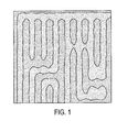
- Fig. 1 illustrates features printed on a substrate suffering from the problem of rippling.
- model-based OPC accounts for mismatch between a target image and predicted image using the following steps.
- a target layer is divided into a plurality of sections.
- a predicted image is evaluated at one "evaluation point" (typically at the center) of each section of the plurality of sections.
- features to be printed are modified by modifying the mask in accordance with the respective evaluation at the center of the corresponding section to minimize the mismatch between the target and predicted image.
- the conventional model based OPC methods accentuate rippling in cases where the evaluation points happen by chance not to be placed in ideally representative locations within their respective sections.
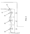
- Fig. 2 illustrates a target image 20 superimposed on a predicted image 22, which has rippling.
- the target image 20 is divided into a plurality of sections 24, and the images 22, 24 are evaluated at evaluation points 26 for each section 24. Each evaluation point 26 is located at the center of the respective section 24.
- the target image is modified (modified mask 30), as illustrated by Fig. 3.
- the modified mask takes into account the mismatch between the target image 20 and predicted image 22.
- an offset of ⁇ n is applied with respect to the target image 20, where n represents the corresponding section 24.
- the resulting new edge is adjusted downwardly in each place where the original predication was high, and is adjusted upwardly in each place where the original prediction was low, as would be expected.
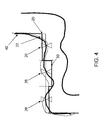
- Fig. 4 illustrates the new predicted image 40 based on the modified mask 30.
- conventional model based OPC techniques accentuates rippling of the new predicted image 40, which increases the likelihood of breaking or bridging depending on surrounding structure.
- the teachings herein alleviate the above noted problems and provide a novel a method of optimizing a design to be formed on a substrate.
- the method includes the steps of determining a deviation between a first representation of the design and a second representation of an image of the design at a plurality of evaluation points for each section of a plurality of sections of the design; determining an amount of modification of the design at each section based on an evaluation of the plurality of evaluation points; and modifying the design at each section by the amount determined in the previous step.
- Further enhancements include identifying a section type for each of the plurality of sections and determining whether each section type corresponds to a corner of the design. When the section type corresponds to the corner, modification of the design at the section corresponding to the corner may not be performed. Alternatively, when the section type corresponds to the corner, it may be determined whether the corner is a concave corner or a convex corner. If the corner is the concave corner, a minimum deviation value from the plurality of evaluation points of the section is determined, and the design is modified at the corner section based on the minimum deviation value. If the corner is the convex corner, the a maximum deviation value is utilized.
- Even further enhancements include determining an evaluation method for each section of the plurality of sections according to each section type, evaluating the deviation at each section according to each evaluation method selected, and modifying the design at each of the plurality of sections based on the results of the evaluations.
- Each evaluation method may be selected from a group consisting of minimum, maximum, middle, mean and median.
- Still further enhancements include for a given section of the plurality of sections, determining the deviation at each of the evaluation points of the given section, determining the deviation at each of a predetermined number of evaluation points of a section adjacent to the given section, and modifying the design at the given section based on an evaluation of the deviation at each of the evaluation points from the two previous steps. Also, the design at a corner section may be modified simply by an adjustment factor.
- Yet even further enhancements include for a given section evaluating the plurality of evaluation points of the given section by determining at least two deviation values comprising a first deviation value for the given section based on a first evaluation method and a second deviation value for the given section based on a second evaluation method, determining a resulting deviation value based on the at least two deviation values, and modifying the design by modifying a design at the given section based on a result of the previous step.
- the first evaluation method may be selected from a group consisting of minimum, maximum, middle, mean and median and the second evaluation method may correspond to a different method selected from the group.
- the novel concepts discussed herein improve model-based OPC for predicted features that have ripples or a waviness characteristic, as shown in Figs. 1-5. Because of the waviness, the inventors have found that by evaluating each section 24 at a plurality of evaluation points 50 (See Fig. 5), and basing the OPC model on these multiple evaluations, errors that occur using the conventional model based OPC techniques can be suppressed.
- Fig. 5 illustrates a target feature 20 and predicted feature 22 similar to that illustrated by Fig. 2.
- the features are divided into a plurality of sections 24.
- evaluations are taken at a plurality of evaluation points 50.
- the number of evaluation points may depend on the complexity of the features to be printed, the amount of rippling, the accuracy desired, the computation time for each section 50 or any combination of the foregoing.
- the disclosed concepts suggest modifying the mask based on multiple evaluations for each corresponding section of the plurality of sections 24.
- the inventors have devised several ways to evaluate error measurements taken for each of the plurality of evaluation points 50; each of which are discussed below.
- any calculation taking into account the multiple evaluation points 50 in each section 24 may be used for determining the necessary correction.
- the deviation error between the target image and the predicted image is determined. These deviation errors are evaluated further to determine necessary modification, if any, to the mask.
- Exemplary calculation methods include determining the average (or taking the arithmetic mean) of the deviation errors for a section, determining the median of the deviation errors of a section. Other examples include choosing the minimum error value or choosing the maximum error value of the evaluations at a section 24. Determining the middle (average of maximum error and minimum error values) may be utilized as well.
- calculation method mentioned above has its advantages. As such, different calculation methods may be employed depending on the features in section 24. In other words, a calculation method may be selected that is best suited for characteristics of the target image and predicted image in the respective section 24.
- Corners are typically divided into two sections, one section for each side, and a plurality of evaluation points are evaluated for each section.
- the mask may be modified according to the minimum deviation error value of the plurality of evaluation points for sections 24 near concave corners whereas the maximum value may be used for sections 24 near convex corners.
- evaluation points of adjacent section(s) 24 may be factored into the calculation for a primary section 24.
- sections 24 may overlap one another, so that a modified mask has more of a smooth transition from a corresponding one section to another.
- an adjustment factor may be applied to evaluations points nearing a corner or at a corner.
- analysis of evaluation points nearing and located at a corner may be obviated entirely.
- the inventors have devised even another method for calculating a correction factor at each section, which includes taking the average of the minimum value, maximum value, and middle result.
- Middle as defined herein, is an average of the maximum and minimum. This has several advantages. Use of minimum-only results in excessive bridging, maximum-only results in excessive pinching, and middle-only avoids excessive pinching and bridging, but does not suppress the rippling effect as average alone does. However, by taking the average of the three, excessive bridging, excessive pinching, and superior suppression of the rippling effect can be accomplished.
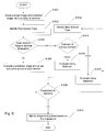
- Fig. 6 illustrates an exemplary flowchart of the evaluation methods described above.
- Step is abbreviated by the letter "S.”
- S 600 a target image and a predicted image (i.e., a representation of the design to be imaged on the substrate and a representation of the image of the design on the substrate, respectively) is divided into a plurality of sections, e.g. the plurality of sections 24 illustrated by Fig. 5.
- the size of each section may depend on the desired accuracy. Smaller sections increasingly reduce the rippling affect but require increased computation time, whereas larger sections do not.
- each section type may be identified. Section types include a corner or those other than a corner. The section type may be identified by manual inspection or software analysis.
- S 604 it is determined whether the section requires special evaluation.
- An example of sections requiring special evaluation may include corner sections. If no special evaluation is required, in S 606 the deviation error at each evaluation point of the section is determined and evaluated. Exemplary evaluation methods were described above to include minimum, maximum, middle, mean and median, as well as other techniques. However, other known evaluation methods may be utilized to determine the amount of modification required for a section.
- S 608 if all sections have been evaluated, the mask is modified in accordance the evaluations. Exemplary modification is illustrated by Fig. 5 (S 610).
- the next section type is identified (S 612). Again, it is determined whether the section that has been identified requires special evaluation (S 604). Considering a corner section, in S 604, it may be determined that a corner requires special evaluation. In S 614, it is determined whether the section is a convex corner or a concave corner. Techniques of identifying whether a section is a convex or a concave section type are well within the level of one of ordinary skill in the art. If the section is concave, the evaluation is performed using the minimum deviation value of the multiple evaluation points (S 616). If the section is convex, the evaluation is performed using the maximum deviation value of the multiple evaluation points (S 618). Once all section evaluations have been completed, the mask is modified by adjusting each section according to the evaluations performed (S 610).
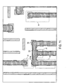
- Figs. 7-11 illustrate simulations performed using minimum, maximum, middle, mean and median calculation methods, respectively.
- the target section is shown by the number 702
- the corrected mask pattern is shown by the number 704
- the predicted printing results by number 706.
- Areas A1-A4 designated in each of the figures have been chosen for comparing the effects of bridging, necking (or pinching), line smoothing, and average line width, respectively.
- Table 1 compiles comparative results for each of the calculation methods simulated and characteristics of the predicted image.
- the predicted pattern using median calculation (Fig. 11) has the best overall characteristics, i . e ., it is the most robust.
- the simulations are representative of the given pattern.
- Other calculation methods may render a best overall predicted pattern for the given pattern.
- other calculation method(s) may be better or best suited for other types of patterns.
- Fig. 12 schematically depicts a lithographic projection apparatus suitable for use with a mask designed with the aid of the current invention.
- the apparatus comprises:
- the apparatus is of a transmissive type (i.e. , has a transmissive mask). However, in general, it may also be of a reflective type, for example with a reflective mask. Alternatively, the apparatus may employ another kind of patterning means as an alternative to the use of a mask; examples include a programmable mirror array or LCD matrix.
- the source LA e.g. a mercury lamp or excimer laser
- This beam is fed into an illumination system (illuminator) IL, either directly or after having traversed conditioning means, such as a beam expander Ex, for example.
- the illuminator IL may comprise adjusting means AM for setting the outer and/or inner radial extent (commonly referred to as ⁇ -outer and ⁇ -inner, respectively) of the intensity distribution in the beam.
- ⁇ -outer and ⁇ -inner commonly referred to as ⁇ -outer and ⁇ -inner, respectively
- it will generally comprise various other components, such as an integrator IN and a condenser CO.
- the beam PB impinging on the mask MA has a desired uniformity and intensity distribution in its cross-section.
- the source LA may be within the housing of the lithographic projection apparatus (as is often the case when the source LA is a mercury lamp, for example), but that it may also be remote from the lithographic projection apparatus, the radiation beam that it produces being led into the apparatus (e.g. with the aid of suitable directing mirrors); this latter scenario is often the case when the source LA is an excimer laser (e.g. based on KrF, ArF or F 2 lasing).
- the current invention encompasses at least both of these scenarios.
- the beam PB subsequently intercepts the mask MA, which is held on a mask table MT. Having traversed the mask MA, the beam PB passes through the lens PL, which focuses the beam PB onto a target portion C of the substrate W. With the aid of the second positioning means (and interferometric measuring means IF), the substrate table WT can be moved accurately, e.g. so as to position different target portions C in the path of the beam PB. Similarly, the first positioning means can be used to accurately position the mask MA with respect to the path of the beam PB, e.g. , after mechanical retrieval of the mask MA from a mask library, or during a scan.
- the mask table MT may just be connected to a short-stroke actuator, or may be fixed.
- the depicted tool can be used in two different modes:
- the concepts disclosed herein may simulate or mathematically model any generic imaging system for imaging sub wavelength features, and may be especially useful with emerging imaging technologies capable of producing wavelengths of an increasingly smaller size.
- Emerging technologies already in use include EUV (extreme ultraviolet) lithography that is capable of producing a 193nm wavelength with the use of a ArF laser, and even a 157nm wavelength with the use of a Fluorine laser.
- EUV lithography is capable of producing wavelengths within a range of 20-5nm by using a synchrotron or by hitting a material (either solid or a plasma) with high-energy electrons in order to produce photons within this range.
- illumination may be produced by reflective mirrors with a multi-stack of Molybdenum and Silicon.
- the multi-stack mirror has a 40 layer pairs of Molybdenum and Silicon where the thickness of each layer is a quarter wavelength. Even smaller wavelengths may be produced with X-ray lithography.
- a synchrotron is used to produce an X-ray wavelength. Since most material is absorptive at x-ray wavelengths, a thin piece of absorbing material defines where features would print (positive resist) or not print (negative resist).
- the concepts disclosed herein may be used as a simulator, i.e. , as a computer program product capable of being implemented on a computer system.
- Software functionalities of the computer system involve programming, including executable code, which may be used to implement the above-described imaging model.
- the software code is executable by the general-purpose computer.
- the code and possibly the associated data records are stored within a general-purpose computer platform.
- the software may be stored at other locations and/or transported for loading into the appropriate general-purpose computer systems.
- the embodiments discussed above involve one or more software products in the form of one or more modules of code carried by at least one machine-readable medium. Execution of such code by a processor of the computer system enables the platform to implement the catalog and/or software downloading functions, in essentially the manner performed in the embodiments discussed and illustrated herein.
- Non-volatile media include, for example, optical or magnetic disks, such as any of the storage devices in any computer(s) operating as one of the server platform, discussed above.
- Volatile media include dynamic memory, such as main memory of such a computer platform.
- Physical transmission media include coaxial cables; copper wire and fiber optics, including the wires that comprise a bus within a computer system.
- Carrier-wave transmission media can take the form of electric or electromagnetic signals, or acoustic or light waves such as those generated during radio frequency (RF) and infrared (IR) data communications.
- Common forms of computer-readable media therefore include, for example: a floppy disk, a flexible disk, hard disk, magnetic tape, any other magnetic medium, a CD-ROM, DVD, any other optical medium, less commonly-used media such as punch cards, paper tape, any other physical medium with patterns of holes, a RAM, a PROM and EPROM, a FLASH-EPROM, any other memory chip or cartridge, a carrier wave transporting data or instructions, cables or links transporting such a carrier wave, or any other medium from which a computer can read programming code and/or data.
- Many of these forms of computer readable media may be involved in carrying one or more sequences of one or more instructions to a processor for execution.
Landscapes
- Physics & Mathematics (AREA)
- General Physics & Mathematics (AREA)
- Exposure And Positioning Against Photoresist Photosensitive Materials (AREA)
- Preparing Plates And Mask In Photomechanical Process (AREA)
- Manufacture Or Reproduction Of Printing Formes (AREA)
- Printing Methods (AREA)
Applications Claiming Priority (2)
| Application Number | Priority Date | Filing Date | Title |
|---|---|---|---|
| US55783304P | 2004-03-31 | 2004-03-31 | |
| US557833 | 2004-03-31 |
Publications (2)
| Publication Number | Publication Date |
|---|---|
| EP1582934A2 true EP1582934A2 (fr) | 2005-10-05 |
| EP1582934A3 EP1582934A3 (fr) | 2007-02-28 |
Family
ID=35539303
Family Applications (1)
| Application Number | Title | Priority Date | Filing Date |
|---|---|---|---|
| EP05252042A Withdrawn EP1582934A3 (fr) | 2004-03-31 | 2005-03-31 | Appareil, méthode et programme pour éviter l'ondulation de structures à imprimer utilisant des systèmes photolithographiques |
Country Status (7)
| Country | Link |
|---|---|
| US (1) | US7856606B2 (fr) |
| EP (1) | EP1582934A3 (fr) |
| JP (1) | JP4727288B2 (fr) |
| KR (1) | KR100847100B1 (fr) |
| CN (1) | CN1749861B (fr) |
| SG (1) | SG115825A1 (fr) |
| TW (1) | TWI385546B (fr) |
Cited By (3)
| Publication number | Priority date | Publication date | Assignee | Title |
|---|---|---|---|---|
| WO2008020265A1 (fr) * | 2006-08-16 | 2008-02-21 | Koninklijke Philips Electronics N.V. | Procédé et appareil de conception d'un circuit intégré |
| EP1720062A3 (fr) * | 2005-05-05 | 2008-07-23 | ASML MaskTools B.V. | Appareil, méthode et programme d'ordinateur pour réaliser le correction de la proximité optique fondée sur un modèle de factorisation l'influence voisine |
| US7962868B2 (en) | 2005-10-28 | 2011-06-14 | Freescale Semiconductor, Inc. | Method for forming a semiconductor device using optical proximity correction for the optical lithography |
Families Citing this family (5)
| Publication number | Priority date | Publication date | Assignee | Title |
|---|---|---|---|---|
| US7707539B2 (en) * | 2007-09-28 | 2010-04-27 | Synopsys, Inc. | Facilitating process model accuracy by modeling mask corner rounding effects |
| US8132128B2 (en) * | 2008-10-31 | 2012-03-06 | Synopsys, Inc. | Method and system for performing lithography verification for a double-patterning process |
| CN104570584B (zh) * | 2013-10-16 | 2019-06-28 | 中芯国际集成电路制造(上海)有限公司 | 一种缺口线端的opc修正方法 |
| US9791786B1 (en) * | 2016-04-08 | 2017-10-17 | Applied Materials, Inc. | Method to reduce line waviness |
| CN117706861A (zh) | 2022-09-08 | 2024-03-15 | 联华电子股份有限公司 | 光掩模结构 |
Family Cites Families (23)
| Publication number | Priority date | Publication date | Assignee | Title |
|---|---|---|---|---|
| JP3331822B2 (ja) | 1995-07-17 | 2002-10-07 | ソニー株式会社 | マスクパターン補正方法とそれを用いたマスク、露光方法および半導体装置 |
| EP0824722B1 (fr) | 1996-03-06 | 2001-07-25 | Asm Lithography B.V. | Systeme d'interferometre differentiel et dispositif lithographique a balayage par etapes pourvu d'un tel systeme |
| JP3551660B2 (ja) | 1996-10-29 | 2004-08-11 | ソニー株式会社 | 露光パターンの補正方法および露光パターンの補正装置および露光方法 |
| WO1998028665A1 (fr) | 1996-12-24 | 1998-07-02 | Koninklijke Philips Electronics N.V. | Dispositif de positionnement bidimensionnellement equilibre a deux porte-objets, et dispositif lithographique comportant ledit dispositif |
| EP0900412B1 (fr) | 1997-03-10 | 2005-04-06 | ASML Netherlands B.V. | Appareil lithographique comprenant un dispositif de positionnement pourvu de deux supports d'objet |
| JPH11121361A (ja) | 1997-10-20 | 1999-04-30 | Canon Inc | 露光方法 |
| JP2000100692A (ja) | 1998-09-21 | 2000-04-07 | Toshiba Corp | 設計パターン補正方法 |
| US6248485B1 (en) | 1999-07-19 | 2001-06-19 | Lucent Technologies Inc. | Method for controlling a process for patterning a feature in a photoresist |
| JP2001159809A (ja) * | 1999-09-21 | 2001-06-12 | Toshiba Corp | マスクパターン設計装置、マスクパターン設計方法およびマスクパターン設計プログラムを格納したコンピュータ読取り可能な記録媒体 |
| JP2001183804A (ja) | 1999-12-24 | 2001-07-06 | Mitsubishi Electric Corp | レイアウト補正装置 |
| US6453457B1 (en) * | 2000-09-29 | 2002-09-17 | Numerical Technologies, Inc. | Selection of evaluation point locations based on proximity effects model amplitudes for correcting proximity effects in a fabrication layout |
| US6625801B1 (en) | 2000-09-29 | 2003-09-23 | Numerical Technologies, Inc. | Dissection of printed edges from a fabrication layout for correcting proximity effects |
| US6665856B1 (en) | 2000-12-01 | 2003-12-16 | Numerical Technologies, Inc. | Displacing edge segments on a fabrication layout based on proximity effects model amplitudes for correcting proximity effects |
| JP2002250999A (ja) | 2001-02-26 | 2002-09-06 | Mitsubishi Electric Corp | パターン補正装置、方法、パターン補正を行うためのコンピュータプログラム、および、そのようなプログラムを記録した記録媒体 |
| JP2003059809A (ja) | 2001-08-20 | 2003-02-28 | Nikon Corp | 露光方法及びデバイス製造方法 |
| US6763514B2 (en) | 2001-12-12 | 2004-07-13 | Numerical Technologies, Inc. | Method and apparatus for controlling rippling during optical proximity correction |
| TWI236574B (en) | 2002-02-08 | 2005-07-21 | Sony Corp | Forming method of exposure mask pattern, exposure mask pattern and manufacturing method of semiconductor device |
| JP4152647B2 (ja) | 2002-03-06 | 2008-09-17 | 富士通株式会社 | 近接効果補正方法及びプログラム |
| JP3871949B2 (ja) | 2002-03-27 | 2007-01-24 | 株式会社東芝 | マスクデータ作成装置及びマスクデータ作成方法 |
| US7043712B2 (en) * | 2003-09-09 | 2006-05-09 | International Business Machines Corporation | Method for adaptive segment refinement in optical proximity correction |
| JP4247104B2 (ja) * | 2003-12-18 | 2009-04-02 | 株式会社東芝 | パターン検証方法、パターン検証システム |
| JP2005215587A (ja) | 2004-02-02 | 2005-08-11 | Sony Corp | 位相シフトマスクの製造方法 |
| JP2009034095A (ja) | 2007-07-06 | 2009-02-19 | Sanyo Chem Ind Ltd | タンパク質含有水溶液安定化剤、タンパク質含有水溶液の安定化方法及びタンパク質含有水溶液 |
-
2005
- 2005-03-30 US US11/092,983 patent/US7856606B2/en active Active
- 2005-03-31 TW TW094110374A patent/TWI385546B/zh not_active IP Right Cessation
- 2005-03-31 KR KR1020050027091A patent/KR100847100B1/ko not_active Expired - Fee Related
- 2005-03-31 SG SG200502034A patent/SG115825A1/en unknown
- 2005-03-31 JP JP2005130357A patent/JP4727288B2/ja not_active Expired - Fee Related
- 2005-03-31 CN CN2005100685372A patent/CN1749861B/zh not_active Expired - Fee Related
- 2005-03-31 EP EP05252042A patent/EP1582934A3/fr not_active Withdrawn
Cited By (4)
| Publication number | Priority date | Publication date | Assignee | Title |
|---|---|---|---|---|
| EP1720062A3 (fr) * | 2005-05-05 | 2008-07-23 | ASML MaskTools B.V. | Appareil, méthode et programme d'ordinateur pour réaliser le correction de la proximité optique fondée sur un modèle de factorisation l'influence voisine |
| US7962868B2 (en) | 2005-10-28 | 2011-06-14 | Freescale Semiconductor, Inc. | Method for forming a semiconductor device using optical proximity correction for the optical lithography |
| WO2008020265A1 (fr) * | 2006-08-16 | 2008-02-21 | Koninklijke Philips Electronics N.V. | Procédé et appareil de conception d'un circuit intégré |
| US8370773B2 (en) | 2006-08-16 | 2013-02-05 | Freescale Semiconductor, Inc. | Method and apparatus for designing an integrated circuit using inverse lithography technology |
Also Published As
| Publication number | Publication date |
|---|---|
| KR100847100B1 (ko) | 2008-07-17 |
| SG115825A1 (en) | 2005-10-28 |
| JP2005316486A (ja) | 2005-11-10 |
| TW200604868A (en) | 2006-02-01 |
| TWI385546B (zh) | 2013-02-11 |
| JP4727288B2 (ja) | 2011-07-20 |
| KR20060045359A (ko) | 2006-05-17 |
| US20060010417A1 (en) | 2006-01-12 |
| US7856606B2 (en) | 2010-12-21 |
| CN1749861B (zh) | 2012-02-29 |
| EP1582934A3 (fr) | 2007-02-28 |
| CN1749861A (zh) | 2006-03-22 |
Similar Documents
| Publication | Publication Date | Title |
|---|---|---|
| US7355681B2 (en) | Optical proximity correction using chamfers and rounding at corners | |
| KR101096143B1 (ko) | Na-시그마 노광세팅 및 디바이스 레이아웃을 이용하는스캐터링 바아 opc에 대한 동시 최적화 방법,프로그램물 및 장치 | |
| US7349066B2 (en) | Apparatus, method and computer program product for performing a model based optical proximity correction factoring neighbor influence | |
| US7485396B2 (en) | Scattering bar OPC application method for sub-half wavelength lithography patterning | |
| US8122391B2 (en) | Method, program product and apparatus for performing double exposure lithography | |
| EP1329771B1 (fr) | Méthode pour optimaliser et calibrer un modèle pour la representation de motifs bidimensionnels | |
| US7493589B2 (en) | Method, program product and apparatus for model based geometry decomposition for use in a multiple exposure process | |
| EP1439420A1 (fr) | Procédé de correction de l'effet de proximité optique assisté par ordinateur pour masques pour trous de contact | |
| EP1901121A2 (fr) | Procédé pour la décomposition d'un motif basée sur l'espacement de traits | |
| US7433791B2 (en) | Method of performing multiple stage model calibration for optical imaging simulation models | |
| EP1582934A2 (fr) | Appareil, méthode et programme pour éviter l'ondulation de structures à imprimer utilisant des systèmes photolithographiques |
Legal Events
| Date | Code | Title | Description |
|---|---|---|---|
| PUAI | Public reference made under article 153(3) epc to a published international application that has entered the european phase |
Free format text: ORIGINAL CODE: 0009012 |
|
| AK | Designated contracting states |
Kind code of ref document: A2 Designated state(s): AT BE BG CH CY CZ DE DK EE ES FI FR GB GR HU IE IS IT LI LT LU MC NL PL PT RO SE SI SK TR |
|
| AX | Request for extension of the european patent |
Extension state: AL BA HR LV MK YU |
|
| PUAL | Search report despatched |
Free format text: ORIGINAL CODE: 0009013 |
|
| AK | Designated contracting states |
Kind code of ref document: A3 Designated state(s): AT BE BG CH CY CZ DE DK EE ES FI FR GB GR HU IE IS IT LI LT LU MC NL PL PT RO SE SI SK TR |
|
| AX | Request for extension of the european patent |
Extension state: AL BA HR LV MK YU |
|
| 17P | Request for examination filed |
Effective date: 20070601 |
|
| AKX | Designation fees paid |
Designated state(s): DE FR GB IT NL |
|
| STAA | Information on the status of an ep patent application or granted ep patent |
Free format text: STATUS: THE APPLICATION IS DEEMED TO BE WITHDRAWN |
|
| 18D | Application deemed to be withdrawn |
Effective date: 20091001 |