EP1587140A2 - Dispositif électronique qui contient un circuit électronique pourvu d'une couche de gel et procédé de fabrication de ce dispositif - Google Patents
Dispositif électronique qui contient un circuit électronique pourvu d'une couche de gel et procédé de fabrication de ce dispositif Download PDFInfo
- Publication number
- EP1587140A2 EP1587140A2 EP05101527A EP05101527A EP1587140A2 EP 1587140 A2 EP1587140 A2 EP 1587140A2 EP 05101527 A EP05101527 A EP 05101527A EP 05101527 A EP05101527 A EP 05101527A EP 1587140 A2 EP1587140 A2 EP 1587140A2
- Authority
- EP
- European Patent Office
- Prior art keywords
- gel
- gel layer
- substrate
- layer
- component according
- Prior art date
- Legal status (The legal status is an assumption and is not a legal conclusion. Google has not performed a legal analysis and makes no representation as to the accuracy of the status listed.)
- Granted
Links
Images

Classifications
-
- H—ELECTRICITY
- H10—SEMICONDUCTOR DEVICES; ELECTRIC SOLID-STATE DEVICES NOT OTHERWISE PROVIDED FOR
- H10W—GENERIC PACKAGES, INTERCONNECTIONS, CONNECTORS OR OTHER CONSTRUCTIONAL DETAILS OF DEVICES COVERED BY CLASS H10
- H10W76/00—Containers; Fillings or auxiliary members therefor; Seals
- H10W76/40—Fillings or auxiliary members in containers, e.g. centering rings
- H10W76/42—Fillings
- H10W76/47—Solid or gel fillings
-
- H—ELECTRICITY
- H02—GENERATION; CONVERSION OR DISTRIBUTION OF ELECTRIC POWER
- H02K—DYNAMO-ELECTRIC MACHINES
- H02K11/00—Structural association of dynamo-electric machines with electric components or with devices for shielding, monitoring or protection
- H02K11/20—Structural association of dynamo-electric machines with electric components or with devices for shielding, monitoring or protection for measuring, monitoring, testing, protecting or switching
-
- H—ELECTRICITY
- H02—GENERATION; CONVERSION OR DISTRIBUTION OF ELECTRIC POWER
- H02K—DYNAMO-ELECTRIC MACHINES
- H02K11/00—Structural association of dynamo-electric machines with electric components or with devices for shielding, monitoring or protection
- H02K11/30—Structural association with control circuits or drive circuits
- H02K11/33—Drive circuits, e.g. power electronics
-
- H—ELECTRICITY
- H02—GENERATION; CONVERSION OR DISTRIBUTION OF ELECTRIC POWER
- H02K—DYNAMO-ELECTRIC MACHINES
- H02K19/00—Synchronous motors or generators
- H02K19/16—Synchronous generators
- H02K19/36—Structural association of synchronous generators with auxiliary electric devices influencing the characteristic of the generator or controlling the generator, e.g. with impedances or switches
- H02K19/365—Structural association of synchronous generators with auxiliary electric devices influencing the characteristic of the generator or controlling the generator, e.g. with impedances or switches with a voltage regulator
-
- H—ELECTRICITY
- H10—SEMICONDUCTOR DEVICES; ELECTRIC SOLID-STATE DEVICES NOT OTHERWISE PROVIDED FOR
- H10W—GENERIC PACKAGES, INTERCONNECTIONS, CONNECTORS OR OTHER CONSTRUCTIONAL DETAILS OF DEVICES COVERED BY CLASS H10
- H10W72/00—Interconnections or connectors in packages
- H10W72/851—Dispositions of multiple connectors or interconnections
- H10W72/874—On different surfaces
- H10W72/884—Die-attach connectors and bond wires
-
- H—ELECTRICITY
- H10—SEMICONDUCTOR DEVICES; ELECTRIC SOLID-STATE DEVICES NOT OTHERWISE PROVIDED FOR
- H10W—GENERIC PACKAGES, INTERCONNECTIONS, CONNECTORS OR OTHER CONSTRUCTIONAL DETAILS OF DEVICES COVERED BY CLASS H10
- H10W90/00—Package configurations
- H10W90/701—Package configurations characterised by the relative positions of pads or connectors relative to package parts
- H10W90/751—Package configurations characterised by the relative positions of pads or connectors relative to package parts of bond wires
- H10W90/753—Package configurations characterised by the relative positions of pads or connectors relative to package parts of bond wires between laterally-adjacent chips
Definitions
- the invention relates to an electronic component and a method for its production and its use according to the preamble of the independent claims.
- Gel systems whose hardness is assigned to this hardness range tend to be Shaking loads to strong gel movements, the electronics to be protected (chips, Bonding wires) damages and leads especially with bonding wires to so-called heel breaks.
- such gel systems exhibit unsatisfactory hardness stabilities occurring high temperature stresses.
- components with soft gels, whose hardness is in the penetration range not completely with gel be covered or coated only with a relatively thin gel layer. she thus remain vulnerable to corrosive media.
- the object of the present invention is to provide an electronic component which a cost effective and effective protection against environmental influences also at Temperature or Scblinbelastitch has.
- the component according to the invention or the method for its production according to the Characteristic features of the independent claims compared to the prior Kunststoff the advantage that corrosion-sensitive areas of the component with a suitable gel coating are sealed so that exposure to Weather conditions on the protected areas is prevented and this Protective effect obtained even at high thermal and mechanical loads remains.
- This is achieved by the component according to the invention having a gel layer, whose Shore00 hardness is located in a range in which the gel on the one hand no plastic deformation under mechanical influences, but also on the other hand not so brittle is that chimney loads of the component to cracks or Lead to separation phenomena. This is especially in a Shore00 hardness range from 40 to 48 points the case.
- the provided with the gel layer component is both high dynamic Requirements as well as thermal cycling and high-temperature or Cryogenic stresses without the need for corrosion protection for corrosion-sensitive components of the component is lost.
- the gel hardness in a medium hardness range becomes a relatively rigid, three-dimensional Network, the dynamic loads, such as those in the Use of electronic control components for generators occur, unempfmdlich reacts and bonding wire heel breaks in bonding wires with a diameter of about 50 microns can be avoided.
- the gel is still insensitive to Usually occurring in the engine compartment media such. For example, oils, antifreeze, Petrol, diesel, cold cleaners or saline deposits.
- the gel layer based on a polydimethylsiloxane, a Polyurethane or an epoxy resin is made, since these materials are particularly robust and resistant to media.
- Particularly suitable are gel systems based on vinyl group-modified polydimethylsiloxanes.
- Another particular advantage of the claimed gel layer is that as well greater layer thicknesses of the gel layer of more than 3 microns can be realized, without that in continuous operation cracks or separation phenomena occur.
- the adhesion promoter layer is based on an alkylvinylsiloxane with glycidoxy or alkoxy termination, a bifunctional silane such as a glycidoxyalkyltrialkoxysilane or a silylated polyglycol.
- FIG. 1 shows a cross section through a Component according to the invention, the corrosion-sensitive areas with a gel layer
- FIG. 2 shows a correlation between the concentration of the hardener in the gel in FIG Wt.% And the resulting Shore00 hardness of the cured gel as a function of Processing temperature
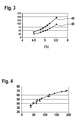
- Figure 3 shows a correlation between the concentration of the hardener in Gel in% by weight and in a measurement of the cured gel with a texture analyzer force to be applied as a function of the processing temperature
- Figure 4 a Correlation of the force determined by a texture analyzer and the corresponding one Shore00 hardness of the gel.
- FIG. 1 shows an electronic component according to the invention in the form of a controller 10 according to a first embodiment of the present invention.
- the Regulator 10 includes a substrate 12 made of, for example, a ceramic material or made of a suitable polymeric material such as PET.
- the substrate 12 is arranged on a heat sink 14, which results in the removal Heat energy is used and made of a suitable, for example metallic material is executed.
- the heat sink 14 is in contact with a housing 16, the simultaneously acts as a boundary of the substrate 12.
- Another Embodiment is that the substrate 12 is part of the housing 16.
- a heat conductive layer 18 is provided, on which a circuit 20, preferably an integrated circuit is located.
- a circuit 20, preferably an integrated circuit On the substrate 12 are still Contact paths 22a, 22b provided, the electrical contacting of the electronic components of the component 10 serve.
- the micromechanical sensor element can, for example, as a pressure sensor be executed.
- the circuit 20 and the additional substrate 24 are, for example, by contacting a first bonding wire 26a with each other.
- the additional substrate 24 electrically contacted via a second bonding wire 26b with the contact track 22a.
- the Circuit 20 is also provided with a third bonding wire 26c with the contact track 22b connected.
- the circuit 20 is used, for example, the control, measured value acquisition and Evaluation of the electronic component in the form of the additional substrate 24th
- the component 10 further comprises a gel layer 28 which supports the substrate 12 on its the heat sink 14 side facing away at least partially covered.
- the gel layer 28 is laterally through the housing 16 and an overflow 30 spatially in their Extension limited.
- the layer thickness of the gel is preferably such that all corrosion-sensitive electronic components such as the circuit 20 and the Additional substrate 24 are enclosed by the gel layer 28.
- the gel layer 28 is preferably based on a Vinyl group modified polydimethylsiloxane performed.
- the production of Gel layer 28 is preferably such that a gel based on a suitable Polysiloxane in the through the housing 16, the substrate 12 and the overflow 30 formed Cavity is filled.
- the gel also contains a suitable hardener on the base a polysiloxane having terminal and optionally further hydride groups.
- the gel may, for example, be designed as a two-component system and have the following exemplary composition: Component A - Vinyl-containing base polymer about 98-99% by weight - bonding agent about 1% by weight - platinum catalyst (organometallic compound) about 0.5% by weight of a Pt-containing stock solution - Inhibitor ⁇ 1% by weight Component B - Vinyl-containing base polymer approx. 84 - 94 wt.% - bonding agent about 1% by weight - Harder about 5 - 15 wt.%
- the gel may further contain fillers, such as fumed silica as a thixotropic agent or silica gel or aluminum oxides.
- the gel layer 28 Since the gel layer 28 is in direct contact with electronic components, must the gel has high ionic purity, especially with respect to its potassium, sodium, Have lithium, chloride or bromide content to contact corrosion and thus to avoid connected electrical faults.
- the gel In a subsequent curing step, the gel at temperatures of 120 to Crosslinked 180 ° C in an oven via a platinum-catalyzed hydrosilylation reaction.
- the concentration of the hardener in the gel is chosen so that the resulting Gel layer 28 after curing a Shore00 hardness of 30 to 50, preferably from 40 to 48 points.
- FIG. 2 shows a plot of the achievable Shore00 hardness of the cured gel the concentration of hardener contained in the gel in% by weight when the gel is applied for one hour a temperature of 120 ° C is cured (curve 40) or when the gel at a Curing temperature of 150 ° C for two hours (curve 42). It will can be seen that a gel hardness in the desired hardness range is achieved when the Concentration of the hardener in the gel between 4.5 and 5.5, in particular between 5.2 and 5.8 wt.% And the curing for one hour at a temperature of 120 ° C. is carried out. If hardening takes place over two hours at a temperature of 150 ° C, the concentration of the hardener in the gel is in a range of 4.5 to 5.2, in particular in a range of 4.7 to 5.2 wt.%.
- Gel hardness measurement via the Texture Analyzer measures the force required is to place a specimen a certain distance into the specimen to be examined to let in.
- This type of measurement of the so-called texture of the specimen is mainly used in the food industry and responds to differences in the food industry Test specimens such as e.g. Layer thickness variances, shape and material as well as influences by Wall or floor effects of the measuring tank very sensitive. For comparability of Measurements therefore need the same specimen with a uniform layer thickness (ie filling quantity) are used.
- the curve 46 shows the achievable hardness analogous to curve 40 when the curing of Gels is carried out for one hour at 120 ° C and curve 48 analogous to curve 42 the attainable hardness, if the gel over two hours at a temperature of one 150 ° C is cured.
- Figure 4 shows a correlation of the over a texture analyzer obtained hardness values with the corresponding Shore00 hardness.
- gel layer 28 contains gel used an adhesion promoter, being used as a primer in particular Compounds are suitable, which are on the one hand an alkoxy group and on the other hand vinyl or Have Si-H groups so that they show the necessary bifunctional character, to solidify both in the three-dimensional polymeric siloxane network of the gel layer 28 to be integrated and at the same time a good adhesion with the materials of the Substrate 12 and the housing 16 or the overflow 30 show.
- an adhesion promoter being used as a primer
- Compounds are suitable, which are on the one hand an alkoxy group and on the other hand vinyl or Have Si-H groups so that they show the necessary bifunctional character, to solidify both in the three-dimensional polymeric siloxane network of the gel layer 28 to be integrated and at the same time a good adhesion with the materials of the Substrate 12 and the housing 16 or the overflow 30 show.
- the substrate 12 may be prior to Applying the gel layer 28 may be provided with a primer layer 32.
- the gel layer 28 produced in this way is suitable for use temperatures between -45 and 150 degrees Celsius and also withstands dynamic loads, such as, for example, a sine-shaker test in the frequency range from 100 to 1000 Hz with an amplitude of 0.19 mm and a maximum acceleration of 300 m / s 2 occur as well as the loads in so-called random-vibration investigations with a maximum acceleration of up to 800 m / s 2 .
- dynamic loads such as, for example, a sine-shaker test in the frequency range from 100 to 1000 Hz with an amplitude of 0.19 mm and a maximum acceleration of 300 m / s 2 occur as well as the loads in so-called random-vibration investigations with a maximum acceleration of up to 800 m / s 2 .
- siloxane gels instead of the described siloxane gels also preferably transparent Polyurethanvergussmassen or epoxy resins are used.
Landscapes
- Engineering & Computer Science (AREA)
- Power Engineering (AREA)
- Microelectronics & Electronic Packaging (AREA)
- Structures Or Materials For Encapsulating Or Coating Semiconductor Devices Or Solid State Devices (AREA)
- Non-Metallic Protective Coatings For Printed Circuits (AREA)
- Micromachines (AREA)
Applications Claiming Priority (4)
| Application Number | Priority Date | Filing Date | Title |
|---|---|---|---|
| DE102004012600 | 2004-03-12 | ||
| DE102004012600 | 2004-03-12 | ||
| DE102004028888A DE102004028888A1 (de) | 2004-03-12 | 2004-06-15 | Elektronisches Bauteil und Verfahren zur Herstellung desselben |
| DE102004028888 | 2004-06-15 |
Publications (3)
| Publication Number | Publication Date |
|---|---|
| EP1587140A2 true EP1587140A2 (fr) | 2005-10-19 |
| EP1587140A3 EP1587140A3 (fr) | 2009-04-01 |
| EP1587140B1 EP1587140B1 (fr) | 2011-09-21 |
Family
ID=34938843
Family Applications (1)
| Application Number | Title | Priority Date | Filing Date |
|---|---|---|---|
| EP05101527A Expired - Lifetime EP1587140B1 (fr) | 2004-03-12 | 2005-03-01 | Dispositif électronique qui contient un circuit électronique pourvu d'une couche de gel et procédé de fabrication de ce dispositif |
Country Status (1)
| Country | Link |
|---|---|
| EP (1) | EP1587140B1 (fr) |
Cited By (3)
| Publication number | Priority date | Publication date | Assignee | Title |
|---|---|---|---|---|
| CN102827542A (zh) * | 2011-06-17 | 2012-12-19 | 罗伯特·博世有限公司 | 用于微芯片的覆盖材料、具有覆盖材料的微芯片以及用于提供这种微芯片的方法 |
| EP2683063A3 (fr) * | 2012-07-03 | 2016-01-06 | Jtekt Corporation | Dispositif de commande et unité de moteur comprenant ledit dispositif |
| CN109650328A (zh) * | 2018-12-17 | 2019-04-19 | 大连理工大学 | 一种动态特性测试的激波底座激励装置及其工作方法 |
Family Cites Families (6)
| Publication number | Priority date | Publication date | Assignee | Title |
|---|---|---|---|---|
| JPS6177353A (ja) * | 1984-09-25 | 1986-04-19 | Toshiba Corp | 半導体整流装置 |
| US5165956A (en) * | 1991-09-27 | 1992-11-24 | At&T Bell Laboratories | Method of encapsulating an electronic device with a silicone encapsulant |
| EP0676450B1 (fr) * | 1994-04-08 | 1999-09-22 | Shin-Etsu Chemical Co., Ltd. | Composition thixotropique d'un gel de silicone fluoré |
| DE19860035A1 (de) * | 1998-12-23 | 2000-07-06 | Trw Automotive Electron & Comp | Elektronikmodul |
| JP3663120B2 (ja) * | 2000-09-04 | 2005-06-22 | 株式会社日立製作所 | 自動車用エンジンコントロールユニットの実装構造及び実装方法 |
| US6614108B1 (en) * | 2000-10-23 | 2003-09-02 | Delphi Technologies, Inc. | Electronic package and method therefor |
-
2005
- 2005-03-01 EP EP05101527A patent/EP1587140B1/fr not_active Expired - Lifetime
Cited By (4)
| Publication number | Priority date | Publication date | Assignee | Title |
|---|---|---|---|---|
| CN102827542A (zh) * | 2011-06-17 | 2012-12-19 | 罗伯特·博世有限公司 | 用于微芯片的覆盖材料、具有覆盖材料的微芯片以及用于提供这种微芯片的方法 |
| EP2683063A3 (fr) * | 2012-07-03 | 2016-01-06 | Jtekt Corporation | Dispositif de commande et unité de moteur comprenant ledit dispositif |
| US9398724B2 (en) | 2012-07-03 | 2016-07-19 | Jtekt Corporation | Control device and motor unit including the control device |
| CN109650328A (zh) * | 2018-12-17 | 2019-04-19 | 大连理工大学 | 一种动态特性测试的激波底座激励装置及其工作方法 |
Also Published As
| Publication number | Publication date |
|---|---|
| EP1587140B1 (fr) | 2011-09-21 |
| EP1587140A3 (fr) | 2009-04-01 |
Similar Documents
| Publication | Publication Date | Title |
|---|---|---|
| EP0019135B1 (fr) | Sonde pour l'application à la mesure de la température ou de la masse d'un milieu en écoulement et procédé pour sa fabrication | |
| Lamaka et al. | Fault-tolerant hybrid epoxy-silane coating for corrosion protection of magnesium alloy AZ31 | |
| DE69736320T2 (de) | Elektronisches kontrollmodul mit flüssigkeitsdichtungen | |
| DE60310222T2 (de) | Halbleiterkapselung und verfahren zu ihrer herstellung | |
| DE60223009T2 (de) | Additionsvernetzbare silikonzusammensetzung gelartiger konsistenz | |
| US6586105B2 (en) | Packaging structure and method for automotive components | |
| DE2913772A1 (de) | Halbleiter-druckwandler | |
| US10519031B2 (en) | Encapsulations for mems sense elements and wire bonds | |
| EP1587140B1 (fr) | Dispositif électronique qui contient un circuit électronique pourvu d'une couche de gel et procédé de fabrication de ce dispositif | |
| DE102004028888A1 (de) | Elektronisches Bauteil und Verfahren zur Herstellung desselben | |
| DE60303643T2 (de) | Härtbare Zusammensetzungen und elektrische/elektronische Teile | |
| DE102012200273A1 (de) | Elektronisches Bauteil mit korrosionsgeschützter Bondverbindung und Verfahren zur Herstellung des Bauteils | |
| DE102007032074A1 (de) | Elektronische Komponenten darin verkapselndes elektronisches Gehäuse | |
| DE10051051A1 (de) | Silikonmodifizierte Einkomponentenvergußmasse | |
| DE102007042976B4 (de) | Drucksensor und Verfahren zu dessen Herstellung | |
| DE10046017B4 (de) | Halbleiter-Drucksensorvorrichtung mit von Schutzelement bedecktem Sensorchip | |
| WO2002033749A1 (fr) | Procede de protection de composants electroniques ou micromecaniques | |
| DE19634845C1 (de) | Verfahren zur Optimierung der Adhäsion zwischen Preßmasse und Passivierungsschicht in einem Kunststoffchipgehäuse | |
| DE19518027C2 (de) | Verfahren zur abstandsgenauen Umhüllung mit funktionstragenden Schichten versehener Bauelemente und danach hergestellte Bauelemente | |
| Pawar et al. | Waterproofing of strain gauges for underwater applications | |
| RU2631820C1 (ru) | Кремнийорганическая композиция для защиты изделий электронной техники | |
| DE9206834U1 (de) | Anschlußteil | |
| DE19839631C1 (de) | Verfahren zum Herstellen eines Temperatursensors | |
| JPS6167247A (ja) | 混成集積回路 | |
| Gentle et al. | Silica/silicone nanocomposite films: A new concept in corrosion protection |
Legal Events
| Date | Code | Title | Description |
|---|---|---|---|
| PUAI | Public reference made under article 153(3) epc to a published international application that has entered the european phase |
Free format text: ORIGINAL CODE: 0009012 |
|
| AK | Designated contracting states |
Kind code of ref document: A2 Designated state(s): AT BE BG CH CY CZ DE DK EE ES FI FR GB GR HU IE IS IT LI LT LU MC NL PL PT RO SE SI SK TR |
|
| AX | Request for extension of the european patent |
Extension state: AL BA HR LV MK YU |
|
| PUAL | Search report despatched |
Free format text: ORIGINAL CODE: 0009013 |
|
| AK | Designated contracting states |
Kind code of ref document: A3 Designated state(s): AT BE BG CH CY CZ DE DK EE ES FI FR GB GR HU IE IS IT LI LT LU MC NL PL PT RO SE SI SK TR |
|
| AX | Request for extension of the european patent |
Extension state: AL BA HR LV MK YU |
|
| 17P | Request for examination filed |
Effective date: 20091001 |
|
| 17Q | First examination report despatched |
Effective date: 20091110 |
|
| AKX | Designation fees paid |
Designated state(s): DE FR GB |
|
| REG | Reference to a national code |
Ref country code: DE Ref legal event code: R079 Ref document number: 502005011906 Country of ref document: DE Free format text: PREVIOUS MAIN CLASS: H01L0023240000 Ipc: H02K0011000000 |
|
| GRAP | Despatch of communication of intention to grant a patent |
Free format text: ORIGINAL CODE: EPIDOSNIGR1 |
|
| RIC1 | Information provided on ipc code assigned before grant |
Ipc: H01L 23/24 20060101ALI20110511BHEP Ipc: H02K 19/36 20060101ALI20110511BHEP Ipc: H02K 11/00 20060101AFI20110511BHEP |
|
| RIN1 | Information on inventor provided before grant (corrected) |
Inventor name: REYES TELLO, LAURA Inventor name: HOLST, MARCO Inventor name: BACHMANN, STEFAN Inventor name: FISCHER, ERWIN |
|
| GRAS | Grant fee paid |
Free format text: ORIGINAL CODE: EPIDOSNIGR3 |
|
| GRAA | (expected) grant |
Free format text: ORIGINAL CODE: 0009210 |
|
| AK | Designated contracting states |
Kind code of ref document: B1 Designated state(s): DE FR GB |
|
| REG | Reference to a national code |
Ref country code: GB Ref legal event code: FG4D Free format text: NOT ENGLISH |
|
| REG | Reference to a national code |
Ref country code: DE Ref legal event code: R096 Ref document number: 502005011906 Country of ref document: DE Effective date: 20111117 |
|
| PLBE | No opposition filed within time limit |
Free format text: ORIGINAL CODE: 0009261 |
|
| STAA | Information on the status of an ep patent application or granted ep patent |
Free format text: STATUS: NO OPPOSITION FILED WITHIN TIME LIMIT |
|
| 26N | No opposition filed |
Effective date: 20120622 |
|
| REG | Reference to a national code |
Ref country code: DE Ref legal event code: R097 Ref document number: 502005011906 Country of ref document: DE Effective date: 20120622 |
|
| PGFP | Annual fee paid to national office [announced via postgrant information from national office to epo] |
Ref country code: FR Payment date: 20130329 Year of fee payment: 9 Ref country code: GB Payment date: 20130318 Year of fee payment: 9 |
|
| PGFP | Annual fee paid to national office [announced via postgrant information from national office to epo] |
Ref country code: DE Payment date: 20140523 Year of fee payment: 10 |
|
| GBPC | Gb: european patent ceased through non-payment of renewal fee |
Effective date: 20140301 |
|
| REG | Reference to a national code |
Ref country code: FR Ref legal event code: ST Effective date: 20141128 |
|
| PG25 | Lapsed in a contracting state [announced via postgrant information from national office to epo] |
Ref country code: FR Free format text: LAPSE BECAUSE OF NON-PAYMENT OF DUE FEES Effective date: 20140331 Ref country code: GB Free format text: LAPSE BECAUSE OF NON-PAYMENT OF DUE FEES Effective date: 20140301 |
|
| REG | Reference to a national code |
Ref country code: DE Ref legal event code: R119 Ref document number: 502005011906 Country of ref document: DE |
|
| PG25 | Lapsed in a contracting state [announced via postgrant information from national office to epo] |
Ref country code: DE Free format text: LAPSE BECAUSE OF NON-PAYMENT OF DUE FEES Effective date: 20151001 |