EP1588377B1 - Circuit differentiel a double grille flottante et procede de programmation - Google Patents
Circuit differentiel a double grille flottante et procede de programmation Download PDFInfo
- Publication number
- EP1588377B1 EP1588377B1 EP04700610A EP04700610A EP1588377B1 EP 1588377 B1 EP1588377 B1 EP 1588377B1 EP 04700610 A EP04700610 A EP 04700610A EP 04700610 A EP04700610 A EP 04700610A EP 1588377 B1 EP1588377 B1 EP 1588377B1
- Authority
- EP
- European Patent Office
- Prior art keywords
- floating gate
- voltage
- circuit
- tunnel
- coupled
- Prior art date
- Legal status (The legal status is an assumption and is not a legal conclusion. Google has not performed a legal analysis and makes no representation as to the accuracy of the status listed.)
- Expired - Lifetime
Links
- 230000009977 dual effect Effects 0.000 title claims abstract description 56
- 238000000034 method Methods 0.000 title claims abstract description 44
- 239000003990 capacitor Substances 0.000 claims description 50
- 230000007423 decrease Effects 0.000 claims description 5
- 238000012545 processing Methods 0.000 claims description 2
- 230000006870 function Effects 0.000 description 34
- 230000005641 tunneling Effects 0.000 description 19
- 238000010586 diagram Methods 0.000 description 16
- 230000008901 benefit Effects 0.000 description 15
- 230000004044 response Effects 0.000 description 14
- 229910021420 polycrystalline silicon Inorganic materials 0.000 description 11
- 229920005591 polysilicon Polymers 0.000 description 11
- 230000000694 effects Effects 0.000 description 10
- 230000008859 change Effects 0.000 description 6
- 239000000758 substrate Substances 0.000 description 6
- 230000008569 process Effects 0.000 description 5
- 239000002784 hot electron Substances 0.000 description 4
- 238000002347 injection Methods 0.000 description 4
- 239000007924 injection Substances 0.000 description 4
- 238000009966 trimming Methods 0.000 description 4
- 230000008878 coupling Effects 0.000 description 3
- 238000010168 coupling process Methods 0.000 description 3
- 238000005859 coupling reaction Methods 0.000 description 3
- 230000008646 thermal stress Effects 0.000 description 3
- 230000005689 Fowler Nordheim tunneling Effects 0.000 description 2
- 230000004888 barrier function Effects 0.000 description 2
- 239000004020 conductor Substances 0.000 description 2
- 230000005684 electric field Effects 0.000 description 2
- 238000012358 sourcing Methods 0.000 description 2
- 238000012360 testing method Methods 0.000 description 2
- 206010073306 Exposure to radiation Diseases 0.000 description 1
- 230000003321 amplification Effects 0.000 description 1
- 238000007796 conventional method Methods 0.000 description 1
- 238000007599 discharging Methods 0.000 description 1
- 239000011810 insulating material Substances 0.000 description 1
- 230000007774 longterm Effects 0.000 description 1
- 230000014759 maintenance of location Effects 0.000 description 1
- 230000005055 memory storage Effects 0.000 description 1
- 238000003199 nucleic acid amplification method Methods 0.000 description 1
- 230000010355 oscillation Effects 0.000 description 1
- 230000035882 stress Effects 0.000 description 1
- 230000002277 temperature effect Effects 0.000 description 1
- 238000012546 transfer Methods 0.000 description 1
Images






Classifications
-
- G—PHYSICS
- G11—INFORMATION STORAGE
- G11C—STATIC STORES
- G11C27/00—Electric analogue stores, e.g. for storing instantaneous values
- G11C27/005—Electric analogue stores, e.g. for storing instantaneous values with non-volatile charge storage, e.g. on floating gate or MNOS
Definitions
- This invention relates to a method and circuit for an accurate voltage reference, and more specifically to a differential circuit that uses a feedback loop and dual conduction of tunnel devices to accurately program a desired charge level on a floating gate.
- a floating gate is an island of conductive material that is electrically isolated from a substrate but capacitively coupled to the substrate or to other conductive layers.
- a floating gate forms the gate of an MOS transistor that is used to read the level of charge on the floating gate without causing any leakage of charge therefrom.
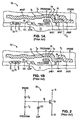
- Fig. 1A is a schematic diagram that illustrates one embodiment of an analog nonvolatile floating gate circuit implemented using two polysilicon layers formed on a substrate and two electron tunneling regions.
- Fig. 1A illustrates a cross-sectional view of an exemplary prior art programmable voltage reference circuit 70 formed on a substrate 71.
- Reference circuit 70 comprises a Program electrode formed from a first polysilicon layer (polyl), an Erase electrode formed from a second polysilicon layer (poly2), and an electrically isolated floating gate comprised of a poly1 layer and a poly2 layer connected together at a corner contact 76.
- polysilicon layers 1 and 2 are separated from each other by a thick oxide dielectric, with the floating gate fg being completely surrounded by dielectric.
- the floating gate fg is also the gate of an NMOS transistor T ⁇ shown at 73, with a drain D and a source S that are heavily doped n+ regions in substrate 70, which is P type.
- tunnel regions 74,75 are typically formed in thick oxide dielectric, they are generally referred to as “thick oxide tunneling devices” or “enhanced emission tunneling devices” Such thick oxide tunneling devices enable the floating gate to retain accurate analog voltages in the +/-4 volt range for many years. This relatively high analog voltage retention is made possible by the fact that the electric field in most of the thick dielectric in tunnel regions 74,75 remains very low, even when several volts are applied across the tunnel device. This low field and thick oxide provides a high barrier to charge loss until the field is high enough to cause Fowler-Nordheim tunneling to occur.
- reference circuit 70 includes a steering capacitor CC that is the capacitance between floating gate fg and a different n+ region formed in the substrate that is connected to a Cap electrode.
- Fig 1B is a schematic diagram that illustrates a second embodiment of a floating gate circuit 70 that is implemented using three polysilicon layers.
- the three polysilicon floating gate circuit 70' is similar to the two polysilicon embodiment except that, for example Erase electrode is formed from a third polysilicon layer (poly 3).
- the floating gate fg is formed entirely from a poly2 layer.
- FIG. 2 shown at 20 is an equivalent circuit diagram for the voltage reference circuit 70 of Fig. 1A and 70' of Fig. 1B.
- each circuit element of Fig. 2 is identically labeled with its corresponding element in Figs. 1A and 1B.
- Setting reference circuit 70 to a specific voltage level is accomplished using two separate operations. Referring again to Fig. 1A, the floating gate fg is first programmed or "reset” to an off condition. The floating gate fg is then erased or “set” to a specific voltage level. Floating gate fg is reset by programming it to a net negative voltage, which turns off transistor T ⁇ . This programming is done by holding the Program electrode low and ramping the n+ bottom plate of the relatively large steering capacitor CC to 15 to 20V via the Cap electrode. Steering capacitor CC couples the floating gate fg high, which causes electrons to tunnel through the thick oxide at 74 from the polyl Program electrode to the floating gate fg. This results in a net negative charge on floating gate fg. When the bottom plate of steering capacitor CC is returned to ground, this couples floating gate fg negative, i.e., below ground, which turns off the NMOS transistor T ⁇ .
- the n+ bottom plate of steering capacitor CC the Cap electrode
- the Erase electrode is ramped to a high voltage, i.e., 12 to 20V.
- Tunneling of electrons from floating gate fg to the poly2 Erase electrode through the thick oxide at 75 begins when the voltage across tunnel device TE reaches a certain voltage, which is typically approximately 11V. This tunneling of electrons from the fg through tunnel device TE increases the voltage of floating gate fg.
- the voltage on floating gate fg then "follows" the voltage ramp coupled to the poly2 Erase electrode, but at a voltage level offset by about 11V below the voltage on the Erase electrode.
- the voltage ramp on poly2 Erase electrode is stopped and then pulled back down to ground. This leaves the voltage on floating gate fg set at approximately the desired voltage level.
- reference circuit 70 meets the requirements for voltage reference applications where approximately 200mV accuracy is sufficient.
- the accuracy of circuit 70 is limited for two reasons. First, the potential on floating gate fg shifts down about 100mV to 200mV after it is set due to the capacitance of erase tunnel device TE which couples floating gate fg down when the poly2 Erase electrode is pulled down from a high voltage to ⁇ V. The amount of this change depends on the ratio of the capacitance of erase tunnel device TE to the rest of the capacitance of floating gate fg (mostly due to steering capacitor CC), as well as the magnitude of the change in voltage on the poly2 Erase electrode.
- Prior art floating gate storage devices have sometimes used dual conduction of Fowler-Nordheim tunnel devices, i.e., wherein both the program and erase tunnel elements in a floating gate device are caused to conduct simultaneously in order to provide the coupling of charge onto the floating gate.
- this method has only been used in digital circuits to program the floating gate to either a "1" condition or a "0" condition to provide memory storage.
- the precise charge on the floating gate in such applications is not of concern and so is not precisely controlled in such circuits.
- such dual conduction digital programming of a floating gate is considered to be a less efficient and desirable way than generating electron conduction through a single tunnel element to control the level of charge on a floating gate.
- Known disadvantages of dual conduction digital programming of a floating gate include the fact that a larger total voltage is required to provide dual conduction and tunnel oxide trap-up is faster because more tunnel current is required.
- U.S. Patent No. 5,059,920 An example of a prior art analog nonvolatile floating gate circuit that uses dual conduction of electrons for adding and removing electrons from a floating gate is disclosed in U.S. Patent No. 5,059,920 , wherein the floating gate provides an adaptable offset voltage input for a CMOS amplifier. In this device, however, only one Fowler-Nordheim tunnel device is used. The electrons are injected onto the floating gate using hot electron injection, while Fowler-Nordheim electron tunneling is used to remove electrons from the floating gate, so as to accurately control the charge on the floating gate. This means of injecting electrons onto the floating gate is used because the charge transfer is a controlled function of the voltage on the floating gate.
- Another example of a prior art dual conduction floating gate circuit is disclosed in U.S. Patent No. 5,986,927 .
- U.S. Patent No. 6,434,051 in Fig. 1 discloses a non-volatile memory circuit, wherein a storage transistor N c that stores information and a feedback transistor N f are commonly connected at a source.
- the storage transistor N c is an N-channel transistor with a floating gate and a control gate.
- the feedback transistor N f is also an N-channel transistor with a floating gate and a control gate.
- a comparator circuit is constructed with transistors N c and N f and load circuits P 0 and P 1 .
- U.S. Patent No. 5,430,670 discloses differential analog memory devices and methods for precisely adjusting the voltages stored on such devices and in particular in FIG. 1A a differential analog memory cell having a pair of floating gates and associated tunnel devices (20a, 22a) as well as coupling capacitors (16, 18).
- a bandgap voltage reference typically provides approximately 25mV absolute accuracy over time and temperature, but can be configured to provide increased accuracy by laser trimming or E 2 digital trimming at test. While a bandgap voltage reference provides greater accuracy and increased stability over the prior art voltage reference circuits discussed above, a bandgap voltage reference only provides a fixed voltage of about 1.2V. Therefore, additional circuitry, such as an amplifier with fixed gain, is needed to provide other reference voltage levels. Moreover, prior art bandgap voltage references typically draw a relatively significant current, i.e., greater than 10 ⁇ A.
- the present invention is directed at addressing the above-mentioned shortcomings, disadvantages, and problems of the prior art.
- the present invention comprises a floating gate circuit, comprising: a) a first floating gate for storing charge thereon; b) a first steering capacitor coupled to said first floating gate for controlling the charge level on said first floating gate as a function of an input set voltage that is coupled through said first steering capacitor to said first floating gate during a set mode; c) a second floating gate for storing charge thereon; d) a first circuit coupled to said second floating gate for controlling the charge level on said second floating gate during said set mode; and e) a feedback circuit coupled between said second floating gate and said first floating gate for causing the charge level on said first floating gate to be modified during said set mode until the voltage on said first floating gate is a predetermined function of the voltage on said second floating gate, and such that at the conclusion of said set mode the difference in charge level between said first and second floating gates is a predetermined function of said input set voltage.
- the floating gate circuit generates a condition at the end of the set mode wherein the voltage on the first floating gate is approximately equal to the voltage on the second floating gate.
- program and erase tunnel devices for the first floating gate operate in dual conduction during the set mode for modifying the charge level on the first floating gate
- program and erase tunnel devices for the second floating gate also operate in dual conduction during the set mode for controlling the voltage on the second floating gate.
- the floating gate circuit can then be configured in a read mode to operate as a voltage reference circuit having a negative feedback loop for causing the floating gate circuit to reach a condition such that a reference voltage is generated that is a predetermined function of the input set voltage, and is preferably approximately equal to the input set voltage.
- the present invention is also a method for setting a reference voltage in a dual floating gate circuit, said method comprising the steps of: a) causing an input set voltage to be capacitively coupled to a first floating gate during a set mode for controlling the charge thereon; b) causing a predetermined voltage to be coupled to a second floating gate during said set mode for controlling the charge level thereon; c) causing the charge level on said first floating gate to be modified until said dual floating gate circuit reaches a condition during said set mode such that the voltage on said floating gate is a predetermined function of the voltage on said second floating gate, and such that at the conclusion of said set mode the difference on charge level between said first and second floating gates is a predetermined function of said input set voltage.
- An object of the present invention is to provide a method and circuit for generating a voltage reference that has an improved accuracy and stability over the prior art voltage references.
- a key advantage of the present invention is the improved initial setting accuracy over prior art floating gate voltage references by more than a factor of 100.
- Another key advantage of the present invention is that, without the need for using laser trimming or E 2 digital trimming, the present invention has an improved accuracy over bandgap voltage references of a factor of 10 to 50 while drawing less power by a factor of more than 10. Moreover, a voltage reference of greater than or less than 1.2 volts can be set using the present invention without the need for additional amplifiers.
- Another advantage of the present invention is that, after a high voltage set mode, the invention allows for a controlled ramp down sequence to ramp down the voltages at each floating gate erase and program electrode such that, when voltage and current sources are completely shut down in the circuit, a more accurate voltage is set on the floating gates.
- Another advantage of the present invention is that the voltage at the erase electrode that is coupled to the reference floating gate is controlled during the ramp down sequence by shutting off the negative voltage charge pump while allowing the feedback circuit to remain active.
- Another advantage of the present invention is that tunnel current is used to self-discharge the voltage at each program electrode.
- Another advantage of the present invention is that any voltage and current offsets coupled through the tunnel devices to the corresponding floating gates and any effects in the transistors used in the floating gate circuit are common mode because of the use of dual floating gates, and do not change the voltage differential produced by the floating gates, and thus do not change the programmed voltage reference at the output during a read mode.
- Yet another advantage of the present invention is that changes in the threshold of transistors in the floating gate circuit due to changes in temperature are also common-mode as the result of the use of two floating gates and therefore have greatly reduced effect on circuit operation.
- Another advantage of the present invention is that changes in source or drain voltages due to bias current, temperature, or power supply voltage variations, which are capacitively coupled to the floating gates, are common-mode and therefore have greatly reduced effect.
- Another advantage of the present invention is that mechanical and thermal stress effects are also common-mode due to the use of two floating gates and so their effects are also greatly reduced.
- Fig. 3 is a circuit diagram of a differential single floating gate circuit 30 for accurately setting a floating gate to an analog voltage during a high voltage set mode or set cycle.
- Fig. 4A is a circuit diagram of a differential dual floating gate circuit 40 according to an embodiment of the present invention. Circuit 40 is also used to accurately set a floating gate to an analog voltage during a high voltage set mode. Once the analog voltage level is set, both circuit 30 and circuit 40 can then be configured during a read mode as a precise voltage comparator circuit with a built-in voltage reference or a precise voltage reference circuit Circuit 30 and circuit 40 are preferably implemented as an integrated circuit manufactured using industry standard CMOS processing techniques. Since the sequence used during the set mode is similar for both circuits, circuit 30 and the method for programming a floating gate using circuit 30 will be described first.
- Circuit 30 comprises a floating gate fg ⁇ at a node 2 that, at the conclusion of a set mode, is set to a voltage that is a function of, and preferably is equal to an input set voltage Vset ⁇ received at an input terminal 300 coupled to a node 1.
- This set mode may be instituted at the factory to cause floating gate fg ⁇ to be set to a desired voltage.
- a later user of circuit 30 can cause circuit 30 to enter a set mode wherever the user wishes to update the voltage on fg ⁇ as a function of the Vset ⁇ voltage input by the user during this later, or in the field, set mode operation.
- Circuit 30 further comprises a circuit 310 that includes: a programming tunnel device TP ⁇ formed between floating gate fg ⁇ and a programming electrode Ep ⁇ , at a node 3; an erase tunnel device Te ⁇ formed between floating gate fg ⁇ and an erase electrode Ee ⁇ , at a node 4; and a steering capacitor C1 coupled between floating gate fg ⁇ and a node 5.
- a programming tunnel device TP ⁇ formed between floating gate fg ⁇ and a programming electrode Ep ⁇ , at a node 3
- an erase tunnel device Te ⁇ formed between floating gate fg ⁇ and an erase electrode Ee ⁇ , at a node 4
- a steering capacitor C1 coupled between floating gate fg ⁇ and a node 5.
- programming electrode Ep ⁇ receives a negative voltage during the set mode
- erase electrode Ee ⁇ receives a positive voltage during the set mode
- Tp ⁇ and Te ⁇ are Fowler-Nordheim tunnel devices that are reasonably well matched by layout.
- the bottom plate of steering capacitor C1 is coupled to a predetermined voltage during the set mode that is preferably ground g1. Steering capacitor C 1 is used to provide a stable ground reference for floating gate fg ⁇ .
- the tunnel devices, Te ⁇ and Tp ⁇ which are reasonably well matched as a result of their chip layout, will modify the charge level on the floating gate fg ⁇ by allowing electrons to tunnel onto and off of floating gate fg ⁇ so as to divide the voltage between nodes 4 and 3 in half.
- the floating gate voltage i.e., the voltage at node 2
- Vfg ⁇ Vnode3 + (Vnode3-Vnode3)/2, which is half way between the voltage at node 4 and the voltage at node 3.
- the dual conduction current can typically charge or discharge node 2, which typically has less than 5 pF capacitance, in less than 1 mSec.
- Vfg ⁇ can be set to a positive or a negative voltage or zero volts depending upon the voltages at electrodes Ee ⁇ and Ep ⁇ . For example, if the tunnel voltage is approximately 11V for the erase and program tunnel devices Te ⁇ and Tp ⁇ , and the voltage at electrode Ee ⁇ is set to about +16V and the voltage at electrode Ep ⁇ is about -6V, then Vfg ⁇ will settle at about +5V, which is the midpoint between the two voltages.
- Vfg ⁇ will go to about ⁇ V. If the voltage at electrode Ee0 is set to about +11V and the voltage at electrode Ep ⁇ is about -11V, then Vfg ⁇ will go to about ⁇ V. If the voltage at electrode Ee ⁇ is set to about +6V and the voltage at electrode Ep ⁇ is about -16V, then Vfg ⁇ will go to about -5V.
- a specific voltage is not generated at node 3 during the set mode.
- the voltage used to control the charge level on floating gate fg ⁇ is the voltage at node 4.
- a current source Ip ⁇ which is preferably implemented as a charge pump, provides the necessary voltage compliance to generate a negative voltage sufficient to generate the voltage difference required to produce dual conduction tunneling in tunnel devices Te ⁇ and Tp ⁇ .
- Circuit 30 further includes a circuit 320 that compares Vfg ⁇ , the voltage on the floating gate fg ⁇ , with the voltage at node 1 and generates an output voltage Vout, at a node 6, that is a function of the difference between Vset ⁇ and the voltage at node 1.
- Circuit 320 preferably includes a differential amplifier (or differential stage) 322 that is preferably configured to have an inverting input coupled to floating gate fg ⁇ , a non-inverting input coupled to node 1, and an output at a node 7.
- Circuit 320 preferably further includes a gain stage 324 with an input coupled to node 7 and an output terminal 326, at node 6.
- the differential stage compares the voltages received at its inputs and amplifies that difference, typically by a factor of 50 to 100.
- the gain stage then further amplifies that difference by another factor of 50 to 100.
- the differential stage 322 preferably includes enhancement mode transistors T1, T2, T3 and T4.
- Transistors T1 and T2 are preferably NMOS transistors that are reasonably well matched by layout, and transistors T3 and T4 are preferably PMOS transistors that are reasonably well matched by layout.
- the sources of NMOS transistors T1 and T2 are coupled together at a node 8.
- the drain of NMOS transistor T1 is coupled to a node 9, and its gate is floating gate fg ⁇ .
- the drain of NMOS transistor T2 is coupled to node 7, and its gate is coupled to node 1.
- PMOS transistor T3 is coupled common drain, common gate, to node 9, with its source coupled to node 10.
- the gate of PMOS transistor T4 is coupled to node 9.
- Vcc typically 3 to 5 volts
- Current source It ⁇ is coupled between node 8 and ground g1 to cause transistors T1, T2, T3 and T4 to operate in either the prethreshold or linear region during the set mode.
- Current source It ⁇ can be implemented using any number of conventional circuits.
- differential stage 322 One benefit provided by differential stage 322 is that temperature and stress effects track in transistors T1-T4 because the temperature coeffcient Tc of these transistors is approximately the same. That is, any variation in the temperature of the integrated circuit chip on which a floating gate circuit according to the present invention is implemented will have the same effect on transistors T1- T4, such that differential stage 322 is in a balanced condition essentially independent of temperature. Similarly, mechanical and thermal stress effects are also common-mode and so their effects are also greatly reduced.
- the gain stage 324 preferably includes a PMOS pull-up transistor T5 biased by Vcc, and includes a current source pull-down load Ig ⁇ .
- the source of transistor T5 is coupled to node 10. Its gate is coupled to the differential stage PMOS pull-up T4 at node 7, and its drain is coupled to node 6.
- Current source pull-down load Ig ⁇ is coupled between node 6 and ground g1.
- the gain stage 324 also preferably includes a compensation capacitor C2 coupled between nodes 6 and 7.
- Current source pull-down load Ig ⁇ is preferably an active load using an NMOS current mirror or a depletion device. Using an active current source with relatively high output resistance, the gain stage 324 can provide a voltage gain of about 100.
- the output swing of the gain stage 324 is nearly full rail from ground to Vcc. Stability and response of this circuit can be easily adjusted for various processes using compensation capacitor C2.
- transistor T5 provides good current sourcing capacity, but current sinking is limited to the current in the current source pull-down Ig ⁇ . Therefore, the current in Ig ⁇ should be greater than the pull-up current required by the load on Vout so that the gain stage 324 is capable of adequately controlling Vout, at node 6, by sinking all of the current that flows to node 6.
- Circuit 320 further operates in the following manner during the set mode.
- T1 senses Vfg ⁇ relative to input set voltage Vset ⁇ (300), which is sensed by transistor T2, and the amplified difference appears as Vout at node 6. If Vfg ⁇ is initially less than Vset ⁇ , T2 is turned on more than T1, and the current flow through T2 (and through T4 since they are connected in series) is initially greater than the current flow through T1 (and correspondingly T3).
- the gate of the pull up transistor T3 is tied to the drain of T3 and also to the gate of pullup transistor T4, which makes the current in T4 a mirror of the current in T3.
- Vfg ⁇ Vset ⁇ .
- circuit 320 can be implemented using PMOS transistors for T1 and T2 and NMOS transistors for T3 and T4.
- the gain stage 324 comprises an NMOS pull-down transistor T5 coupled to a current source pull-up load Ig ⁇ .
- Circuit 30 also includes a feedback loop coupled between nodes 6 and 2. During the set mode, this feedback loop causes the voltage differential between tunnel electrodes Ee ⁇ and Ep ⁇ to be modified by modifying the voltage at node 4 as a function of the output voltage at node 6.
- the feedback loop preferably comprises a level shift circuit that is preferably a tunnel device TF ⁇ formed between node 6 and a node 11 and a transistor T7, preferably an NMOS transistor, coupled common gate, common drain to a node 12, with its source coupled to node 11. Also included in the feedback loop is a transistor T6, preferably an NMOS transistor, having its gate coupled to node 12, its source coupled to node 4, and thereby to erase tunnel device Te ⁇ , and its drain coupled to a node 13.
- the maximum output of the gain stage is approximately Vcc.
- Vout the relatively low output voltage at node 6 (Vout) up to the desired 14 to 19 volt range.
- TF ⁇ and Te ⁇ are reasonably well matched by layout and transistors T6 and T7 are reasonably well matched by layout.
- the level shift tracks the erase tunnel voltage as measured by the voltage drop from node 4 to node 2, which drives the gate of transistor T1 (fg ⁇ ) to the same voltage as the voltage on the gate of transistor T2 (Vset ⁇ ) when circuit 320 settles. This adds to the improved setting accuracy of the circuit.
- One advantage of having the level shift track the erase tunnel voltage is that, as the voltage necessary to create tunneling changes, due to charge trapping in the dielectric as more and more set cycles are performed, output voltage Vout continues to follow the input set voltage V set ⁇ and operate in the same voltage range.
- Another advantage is that when the output voltage Vout is not quite equal to the input set voltage Vset ⁇ , the error introduced by the finite gain of circuit 320 is very small. For example, if circuit 320 has a gain of 10,000 and Vout is 1 volt lower than Vset ⁇ and Vfg ⁇ when circuit 30 settles, Vfg ⁇ will have an error of 1V/10,000, or only 0.1mV.
- Circuit 30 also preferably includes current sources 12 and Ip ⁇ , and a capacitor Cp ⁇ .
- Current source 12 is coupled between node 12 and a high voltage supply HV+ at node 13 for establishing Vefb at the beginning of the set mode and for providing tunnel current through TF ⁇ .
- Current source I2 can be implemented using any number of conventional methods. However, current source I2 is preferably a current regulator that is biased by HV+, such as a current mirror comprising P-Channel devices that operate in the prethreshold region. In this manner, current source 12 will automatically go to whatever positive voltage needed at node 12 to establish the tunnel current through tunnel device TF ⁇ .
- Current source 12 preferably generates a current that is about the same as Ip ⁇ . This means the current through tunnel device TF ⁇ is about the same as the current through tunnel devices Te ⁇ and Tp ⁇ .
- Current source Ip ⁇ is coupled between node 3 and ground g1
- Current source Ip ⁇ is preferably a P-Channel charge pump that is used as a negative current source to pump a controlled tunnel current out of programming tunnel device Tp ⁇ .
- Ip ⁇ since Ip ⁇ is a current source, it functions to automatically goes to whatever negative voltage at node 3 that is needed to establish the tunnel current at the desired level.
- Current source Ip ⁇ has sufficient voltage compliance to provide this negative voltage.
- the voltage across the tunnel devices is also well defined by their Fowler-Nordheim characteristics. Therefore, current source Ip ⁇ produces Vp, the voltage at node 3, by controlling the current through tunnel device Tp0.
- a current source Ip ⁇ is the preferred way to assure that tunnel devices Te ⁇ and Tp ⁇ are operating at a current level that is high enough to allow dual conduction and to allow the feedback circuit to work, but low enough to avoid excessive current flow which damages the tunnel devices.
- Capacitor Cp ⁇ controls the discharge of current through the tunnel devices when, as explained in more detail below, Ip ⁇ is shut down at the conclusion of the set mode.
- Vp can also be produced using a fixed voltage supply that is about 24 to 30 volts below Vefb.
- this topology should be used with caution because the current in Fowler-Nordheim tunnel devices varies exponentially with the applied voltage.
- very high current will flow through the tunnel devices if the voltage differential is too high, and extremely low current may flow if the voltage differential is too low.
- Very high currents will damage or "wear out" the tunnel devices due to rapid charge trapping in the dielectric, and if the tunnel current is too low, the feedback circuit will not be able to tunnel charge onto or off of fg ⁇ , and thus will not be able to control the voltage on fg ⁇ .
- Vp controls the voltage on fg ⁇ .
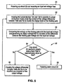
- Fig. 5 is a flow diagram illustrating a method 50 for setting a floating gate that may be implemented during a set mode, for instance, by circuit 30 of Fig. 3.
- Figs. 6-8 illustrate voltage waveforms for Vout, Vp, Vefb, Vfg ⁇ and Vset ⁇ , for the specific implementation of method 50 discussed below relative to those figures.
- Each of the four waveforms shown in Figs. 6-8 are the same, only the voltage axes of some of these waveforms are modified to illustrate specific details.
- Vset ⁇ 4.00V
- Vcc +5V
- HV+ is about 22V
- Ip0 is about 6nA
- I2 is about 6nA
- It ⁇ is about 5nA
- Ig ⁇ is about 20nA.
- circuit 30 is powered up at the beginning of the set mode, which is illustrated in Figs. 6-8 as time t 0 , and at some point thereafter receives input set voltage Vset ⁇ .
- Figs. 6-8 further illustrate Vset ⁇ being held at a constant voltage of 4.00V.
- Vcc is set to +5V
- HV+ is ramped up to a high positive voltage of about +22V, which turns on 12
- current source Ip ⁇ is turned on to enable this current source to begin generating its corresponding current.
- circuit 30 can set Vfg ⁇ to within about 0.5 mV of Vset ⁇ in about 30 mSec, as illustrated in Figs. 6-8.
- circuit 30 causes tunnel devices Te ⁇ and Tp ⁇ to operate in a dual conduction mode under the control of the voltage differential between the erase and programming electrodes Ee ⁇ and Ep ⁇ , respectively, for modifying the charge level on floating gate fg ⁇ . Dual conduction occurs when tunnel current flows through both Te ⁇ and Tp ⁇ . Tunnel current flows through Te ⁇ and Tp ⁇ when the voltage differential between the erase and programming electrodes is at least two tunnel voltages or approximately 22V as discussed earlier.
- circuit 30 causes dual conduction in the following manner.
- Current source 12 pulls node 12, Vefb, up relatively quickly to about +18V.
- Vefb (node 12) turns on transistor T6, which pulls Ve ⁇ (node 4) to one Vt below Vefb.
- Charge pump Ip ⁇ gradually charges capacitor Cp ⁇ and ramps Vp (node 3) down to a negative voltage of about -11V in about 2 mSec. Once Vp ramps down to the point where the difference between Ve ⁇ and Vp is at least two tunnel voltages, tunnel current flows through both tunnel devices Te ⁇ and Tp ⁇ , under the control of Ip ⁇ , and Vfg ⁇ is controlled directly by Vefb.
- circuit 30 compares Vfg ⁇ with Vset ⁇ and generates an output voltage Vout that is a function of the difference between Vfg ⁇ and Vset ⁇ .
- Circuit 30 then, at step 55, causes the voltage differential between Vefb and Vp to be modified as a function of Vout, by modifying Vefb, and circuit 30 repeats steps 52 through 55 until circuit 30 settles to a steady state condition, at step 54, where Vfg ⁇ is approximately equal to Vset ⁇ . At this point circuit 30 is powered down, at step 56. As a result of method 50, fg ⁇ is set to a charge level that will remain essentially the same over time.
- Vfg ⁇ is below Vset ⁇ .
- transistor T1 is OFF and transistor T2 is ON, which pulls down node 7.
- This turns on transistor T5, which quickly pulls up Vout from zero volts, also illustrated in Fig. 6.
- tunnel current is flowing through TF ⁇
- TF ⁇ and T7 act as level shifters such that Vefb pulls up 1TV and 1Vt above Vout. Vefb then pulls up Vfg ⁇ through tunnel device Te ⁇ . Since Vp is continuing to ramp down to a predetermined negative voltage, Vfg ⁇ is pulled greater than Vset ⁇ after about 1 mSec.
- the differential stage 322 senses that Vfg ⁇ is greater than Vset ⁇ , and the gain stage 324 amplifies that difference, quickly pulling Vout low, which pulls Vefb low and pulls Vfg ⁇ back down low.
- Vfg ⁇ is approximately equal to Vset ⁇
- circuit 320 ceases to oscillate except for some noise coupled to circuit 320 from the charge pump Ip ⁇ as best shown in Figs. 7 and 8 beginning at time t 2 .
- current source Ig ⁇ in the gain stage 324 produces a current that is much larger than that generated by current source I2. Therefore, the gain stage 324 is able control Vout by sinking all the current from I2 that flows through T7 and TF ⁇ to Vout.
- the compensation capacitor C2 in the gain stage 324 is made large enough to assure the feedback loop is stable and settles in less than about 1 mSec.
- the level shift in Vefb caused by the Vt across T7 approximately matches the voltage drop in T6.
- the level shift in Vefb caused by the tunnel voltage across TF ⁇ approximately matches the voltage drop across tunnel device Te ⁇ , so that when the differential and gain stages settle, Vfg ⁇ and Vout are about the same. This can be seen in Fig.
- Vout settles to within about 30mV of Vfg ⁇ , beginning at time t 2 .
- This 30mV difference is generated by noise coupled to fg ⁇ from the Ip ⁇ current source.
- negative charge pump Ip0 which pumps charge from the program tunnel device Tp0, produces noise on Vp.
- This noise is coupled to floating gate fg ⁇ through program tunnel device capacitance Cp ⁇ .
- the noise on Vp cannot be seen in the Vp waveform in Fig. 8 because the voltage axis is shown in volts, whereas the voltage axis for the Vfg ⁇ vs. Vset ⁇ waveform is shown in millivolts.
- Step 56 may be performed by simply concurrently shutting off the charge pump Ip ⁇ and HV+, and thereby current source 12, at time t 3 . However, this may significantly impact Vfg ⁇ once Vefb and Vp have ramped back to 0V. As explained above, noise from Ip ⁇ limits the accuracy of setting Vfg ⁇ equal to Vset ⁇ when the negative charge pump that generates Vp is ON.
- Vfg ⁇ may not be equal to Vset ⁇ at the beginning of the ramping of Vefb and Vp to ground. If Vfg ⁇ is not equal to Vset ⁇ when this ramp down begins, then Vfg ⁇ will not equal Vset ⁇ after Vp and Vefb reach ⁇ V. Moreover, during the ramp down, the current that continues to flow through tunnel devices Te ⁇ and Tp ⁇ is typically not the same. This further affects the final charge level on floating gate fg ⁇ .
- the current in the erase and program tunnel devices must be the same during this time.
- the voltage across each of the tunnel devices must be the same, which means Vefb must ramp down to ⁇ V at the same rate as Vp ramps up to ⁇ V.
- the tunnel device characteristics must be well matched.
- circuit 30 should be powered down, at step 56, in the following preferred manner.
- Ip ⁇ is shut off at t 3 to eliminate the pump noise.
- HV+ and thereby current source 12 are left on such that the feedback circuit is still active and continues to control Vefb.
- tunnel current continues to flow through Te ⁇ and Tp ⁇ as Cp ⁇ discharges, which pulls up Vp back towards ⁇ V. This tunnel current and the capacitance Cp ⁇ determine the ramp rate on Vp.
- Circuit 320 senses Vfg ⁇ moving upwards and ramps Vefb down towards ⁇ V through the feedback circuit.
- Vefb ramps down and Vp ramps up the tunnel current in tunnel devices Te ⁇ and Tp ⁇ decreases rapidly due to the steep slope of their Fowler-Nordheim tunnel device characteristics. Since feedback response time depends directly on the current in the erase tunnel device, the feedback circuit response slows down as Vefb ramps down. As the tunnel current decreases, both the ramp rate and feedback response times slow down and Vfg ⁇ gradually moves closer to Vset ⁇ . For instance, Fig.
- Vfg ⁇ has converged to within about 0.5 mV of Vset ⁇ for a set mode time of 30 mSec, and Vfg ⁇ may be set even more accurately by allowing a ramp down time of greater than 30 mV.
- the HV+ voltage supply and thereby the I2 current source can be shut off, for instance at t 4 , without affecting the charge on fg ⁇ .
- Vcc may be shut off. In other words, once Vfg ⁇ is detected as being within a predetermined threshold level of Vset ⁇ , a steady state condition has been reached and power to circuit 30 can be shut off without affecting the value of Vfg ⁇ .
- Vfg ⁇ is always slightly above Vset ⁇ so circuit 320 and the feedback circuit continue to ramp Vefb down. If Vfg ⁇ goes below Vset ⁇ and the feedback switches the direction Vefb is ramping, the feedback system will start to oscillate very slowly and Vfg ⁇ will diverge from Vset ⁇ instead of converge towards Vset ⁇ . After Vefb and Vp have ramped a few volts towards ⁇ V and Vfg ⁇ is very close to Vset ⁇ , Vefb and Vp can be ramped to ⁇ V quickly, as illustrated at time t 4 in Fig.
- Cp ⁇ is designed such that the feedback response time is slightly slower than the discharge rate of Cp ⁇ .
- Cp ⁇ should be set at about 2.4pf.
- floating gate fg ⁇ will then continue to indefinitely store the charge level programmed on floating gate fg ⁇ during the set mode, subject to possible charge loss, e.g., due to detrapping of electrons or dielectric relaxation over time, without any external power being supplied to circuit 30.
- Vfg ⁇ was set to be equal to Vset ⁇
- circuit 30 can be configured such that Vfg ⁇ is set to a voltage that is some other predetermined value of Vset ⁇ .
- Circuit 40 preferably comprises a reference floating gate fgr at a node 15 and a second floating gate fg1 at a node 14.
- both floating gates fgr and fg1 are programmed, respectively, to charge levels such that the difference in charge level between fgr and fg1 is a function of an input set voltage capacitively coupled to fgr during the set mode.
- circuit 40 may be configured as a voltage reference circuit such that an output reference voltage is generated that is a function of the input set voltage and is preferably equal to the input set voltage.
- the set mode may be instituted at the factory to cause fgr and fg1 to be set to their respective desired charge levels, and thereby, to cause circuit 40 to generate a desired output reference voltage whenever circuit 40 is later caused to enter its read mode.
- a later user of circuit 40 can cause circuit 40 to enter a set mode whenever the user wishes, to thereby update the difference in charge levels between fgr and fg1 as a function of the Vset ⁇ voltage input and thus to update the output reference voltage generated by circuit 40 during subsequent read mode.
- the sequence used to program floating gates fgr and fg1 in circuit 40 is similar to the sequence used to set the charge level on floating gate fg ⁇ in circuit 30 of Fig. 3.
- One major difference between the previously described single floating gate circuit 30 and the dual floating gate circuit 40 is that the gate of transistor T2 in Fig. 3 is replaced by a floating gate, fg1, in Fig. 4A, that cannot be connected directly to an external voltage.
- a voltage Vx is coupled at a node 27 to the gate of a transistor T15 in circuit 40, such that Vfg1 is set to Vx-1Vt-1TV, where 1 Vt is the threshold voltage of transistor T15 and 1TV is the tunnel voltage of an erase tunnel device Te1.
- Vx is generated by a second floating gate voltage reference circuit, e.g., circuit 30.
- Fig. 4B is a combined schematic and block diagram illustrating this embodiment. Circuits 30 and 40 in Fig. 4B are identical to the circuits illustrated, respectively, in Figs. 3 and 4A. In the embodiment shown in Fig. 4B, a high voltage set cycle is performed on both the single floating gate differential circuit 30 and the dual floating gate differential reference circuit 40 at the same time. During the set mode, circuit 30 generates the voltage at node 12 such that floating gate fg ⁇ is set as described earlier, wherein Vset ⁇ for circuit 30 is an internally or externally supplied predetermined voltage, such as +4v.
- Floating gate fg1 is therefore set to a voltage that is a predetermined function of the voltage on floating gate fg ⁇ , and is preferably set to be approximately equal to Vfg ⁇ assuming the tunnel devices in both differential circuits, i.e., circuits 30 and 40, are reasonably well matched.
- the voltage set on floating gate fg1 is then used to set the voltage on floating gate fgr, such that Vfgr is a predetermined function of Vfg1, and preferably approximately equal to Vfg1, as described in greater detail below.
- Circuit 40 further comprises a circuit 410 that includes: a programming tunnel device Tpr formed between floating gate fgr and a programming electrode Epr, at a node 16; an erase tunnel device Ter formed between floating gate fgr and an erase electrode Eer, at a node 17; and a steering capacitor Cfgr coupled between floating gate fgr and a node 18.
- Circuit 40 also comprises a circuit 420 that includes: a programming tunnel device Tp1 formed between floating gate fg1 and a programming electrode Ep1, at node 16, and an erase tunnel device Te1 formed between floating gate fg1 and an erase electrode Ee1, at a node 28.
- programming electrodes Epr and Ep1 receive a negative voltage during the set mode
- erase electrodes Eer and Ee 1 receive a positive voltage during the set mode
- tunnel devices Tpr, Tp1, Ter and Te1 are preferably Fowler-Nordheim tunnel devices that are reasonably well matched as a result of their chip layout, and these tunnel devices are ideally reasonably well matched with tunnel devices Tp0 and Te ⁇ of circuit 30.
- circuit 40 Also included in circuit 40 is a steering capacitor Cfg1 coupled between floating gate fg1 and a node 32.
- the bottom plate of steering capacitor Cfg1 is coupled to a predetermined voltage during the set mode that is preferably ground g1.
- Steering capacitor Cfg1 is used to provide a stable ground reference for floating gate fg1.
- Circuit 40 also includes a transistor T15 that has its drain coupled to a high voltage supply HV+, at a node 26, its source coupled to node 28, and its gate coupled to node 27.
- Setting a voltage on floating gate fgr during the set mode is achieved by taking electrode Epr negative and electrode Eer positive such that the voltage at node 17 minus the voltage at node 16 is two tunnel voltages or approximately 22V.
- the dual conduction current at 22V is typically approximately one to two nanoamps.
- An alternative is to create a sufficient voltage differential across electrode Epr and electrode Eer to generate a current flow of approximately 5nA from node 16 to node 17.
- both tunnel devices are conducting, i.e., the tunnel devices are in "dual conduction.”
- the voltage on the floating gate fgr can stabilize at a DC voltage level for as long a time as needed to enable circuit 40 to end the set mode process in a controlled fashion such that the voltage on floating gate fgr settles to a very precise and accurate level.
- Operating in dual conduction with feedback through at least one of the tunnel devices is key to making it possible to set the floating gate fgr voltage very accurately.
- the tunnel devices Ter and Tpr which are reasonably well matched by layout, will modify the charge level on floating gate fgr by allowing electrons to tunnel onto and off of floating gate fgr so as to divide the voltage between nodes 17 and 16 in half.
- the floating gate voltage i.e., the voltage at node 15
- Vfgr Vnode16 + (Vnode17-Vnode16)/2, which is half way between the voltage at node 17 and the voltage at node 16.
- the dual conduction current can typically charge or discharge node 15, which typically has less than 1.0 pF capacitance, in less than 1 mSec.
- Vfgr can be set to a positive or negative voltage or zero volts depending upon the value of the voltages existing at electrodes Eer and Epr. For example, if the tunnel voltage is approximately 11 V for the erase and program tunnel devices Ter and Tpr, and the voltage at electrode Eer is set to about +16V and the voltage at electrode Epr is set to about -6V, then Vfgr will settle at about +5V, which is the midpoint between the two voltages.
- Vfgr will go to about ⁇ V. If the voltage at Eer is set to about +6V and the voltage at Epr is set to about -16V, then Vfgr will go to about -5V.
- circuit 40 programs both floating gates fgr and fg1 during the set mode.
- tunnel devices Tp1 and Te1 similarly operate in dual conduction to modify the charge level on floating gate fg1 by allowing electrons to tunnel onto and off of floating gate fg1 so as to divide the voltage between nodes 28 and 16 in half.
- Circuit 40 further includes a circuit 430 that compares Vfgr, the voltage on floating gate fgr to Vfg1, the voltage on floating gate fg1, and that generates an output voltage Vout, at node 19, that is a function of the difference between the voltages on floating gates fgr and fg1.
- Circuit 430 preferably includes a differential amplifier (or differential stage) 432 that is preferably configured to have a non-inverting input coupled to floating gate fg1 and an inverting input coupled to floating gate fgr.
- Circuit 430 further includes a gain stage 434 with an input coupled to node 20 and an output terminal 436, at node 19.
- the differential stage 432 compares the voltages received at its inputs and amplifies that difference, typically by a factor of 50 to 100.
- the gain stage 434 then further amplifies that difference by another factor of 50 to 100.
- the differential stage 432 preferably includes enhancement mode transistors T8, T9, T10 and T11.
- Transistors T8 and T9 are preferably NMOS transistors that are reasonably well matched by layout, and transistors T10 and T11 are preferably PMOS transistors that are reasonably well matched by layout.
- the sources of NMOS transistors T8 and T9 are coupled together at a node 21.
- the drain of NMOS transistor T8 is coupled to a node 22, and its gate is floating gate fgr.
- the drain of NMOS transistor T9 is coupled to a node 20, and its gate is floating gate fg1.
- PMOS transistor T10 is coupled common drain, common gate, to node 22, with its source coupled to a node 23.
- the gate of PMOS transistor T11 is coupled to at node 22. Its drain is coupled to node 20, and its source is coupled to node 23.
- a voltage supply Vcc typically 3 to 5 volts, is coupled to node 23, and a current source Itr is coupled between node 21 and ground g1 to cause transistors T8, T9, T10 and T11 to operate in either the pretheshold or linear region during the set mode.
- Current source Itr can be generated using any number of conventional circuits.
- the gain stage 434 preferably includes a PMOS pullup transistor T12 biased by Vcc and a current source pull-down load Igr.
- the source of transistor T12 is coupled to node 23. Its gate is coupled to the differential stage pull-up transistor T11 at node 20, and its drain is coupled to node 19.
- Current source pull-down load Igr is coupled between node 19 and ground g1.
- the gain stage 434 also preferably includes a compensation capacitor C3 coupled between nodes 19 and 20.
- Current source pull-down load Igr is preferably an active load using an NMOS current mirror or a depletion device. Using an active current source with relatively high output resistance, the gain stage 434 can provide a voltage gain of about 100.
- the output swing of the gain stage 434 is nearly full rail from ground to Vcc. Stability and response of this circuit can be easily adjusted for various processes using compensation capacitor C3.
- transistor T12 provides good current sourcing capability, but current sinking is limited to the current in the current source pull-down Igr. Therefore, the current in Igr should be greater than the pull-up current required by the load on Vout so that the gain stage 434 is capable of adequately controlling Vout by sinking all of the current that flows to Vout.
- Circuit 430 further operates in the following manner.
- T8 senses Vfgr relative to Vfg1, which is sensed by transistor T9, and the amplified difference appears as Vout at node 19. If Vfgr is initially less than Vfg1, T9 is turned on more than T8, and the current flow through T9 (and through T11 since they are connected in series) is initially greater than the current flow through T8 (and correspondingly T10).
- the gate of the pullup transistor T10 is tied to the drain of T10 and also to the gate of pullup transistor T11, which makes the current in T11 a mirror of the current in transistor T10.
- the voltage, V20, on node 20 drops below the voltage V22, on node 22.
- the lower voltage on node 20 causes the current through transistor T12 to increase, which pulls Vout high.
- the voltage gain of the differential stage 432 is typically about 80 and the voltage gain of the gain stage 434 is typically about 100 giving an overall gain from Vfg1 to Vout of about 8000.
- a negative feedback path from Vout to the inverting input fgr is necessary for circuit 430 to settle at the point where the voltage on fgr is equal to the voltage on fg1. During the set mode, this feedback path is provided by tunnel devices TF1 and Ter and transistors T13 and T14 as described in the next section.
- Vfgr Vfg1.
- circuit 430 can be implemented using PMOS transistors for T8 and T9 and NMOS transistors for T10 and T11.
- the gain stage 434 preferably comprises an NMOS pull-down transistor T12 coupled to a current source pull-up load Igr.
- Circuit 40 also includes a feedback loop coupled between nodes 19 and 15. During the set mode, this feedback loop causes the voltage differential between tunnel electrodes Eer and Epr to be modified by modifying the voltage at node 17 as a function of the voltage at node 19.
- the feedback loop preferably comprises a level shift circuit, preferably a tunnel device TF1 formed between node 19 and a node 24, and a transistor T14, preferably an NMOS transistor, coupled common gate, common drain at a node 25, with its source coupled to node 24.
- a transistor T 13 preferably an NMOS transistor, having its gate coupled to node 25, its source coupled to node 17, and thereby to erase tunnel device Ter, and its drain coupled to node 26.
- the maximum output of the gain stage 434 is approximately Vcc. However, this is not high enough to drive the voltage at node 25 (Vefb) directly, because Vefb typically needs to go to about 14 to 19 volts, which is well above the usual 3 to 5 volt Vcc supply level.
- the level shift circuit TF1 and T14 shifts the low output voltage at node 19 (Vout) up to the desired 14 to 19 volt range.
- TF1 and Ter are reasonably well matched by layout and T13 and T14 are reasonably well matched by layout.
- the level shift tracks the erase tunnel voltage as measured by the voltage drop from node 17 to node 15 which drives the gate of transistor T8 (fgr) to the same voltage as the voltage on the gate of transistor T9 (fgl)when circuit 430 settles. This adds to the improved setting accuracy of the circuit.
- One advantage of having the level shift track the erase tunnel voltage is that, as the voltage necessary to create tunneling changes, due to charge trapping in the dielectric as more and more set cycles are performed, the circuit 430 output, Vout, continues to follow Vfg1 and operate in the same voltage range.
- Another advantage is that when the output voltage Vout is not equal to Vfgr, the error introduced by the finite gain of circuit 430 is very small. For example, if circuit 430 has a gain of 10,000 and Vout is 1 volt lower than Vfg1 minus Vfgr when circuit 40 settles, Vfg1 minus Vfgr will have an error of 1V/10,000, or only 0,1mV.
- Circuit 40 also preferably includes current sources I2r and Ipr, and a capacitor Cpr.
- Current source I2r is coupled between node 25 and HV+ at node 26 for establishing Vefb at the beginning of the set mode and for providing tunnel current through TF1.
- Current source 12r can be implemented using any number of conventional circuits.
- current source I2r is preferably a current regulator that is biased by HV+, such as a current mirror comprising P-Channel devices that operate in the prethreshold region. In this manner, current source I2r will automatically go to whatever positive voltage is needed at node 25 to establish the tunnel current through tunnel device TF 1.
- current source I2r preferably generates a current that is about half that of current source Ipr, so that the current through tunnel device TF1 is about the same as the current through tunnel devices Ter, Tpr, Te1, and Tp1.
- Current source Ipr is coupled between node 16 and ground g1.
- Current source Ipr is preferably a P-Channel charge pump that is used as a negative current source to pump a controlled tunnel current out of programming tunnel devices Tpr and Tp1. Since Ipr is a current source, it automatically goes to whatever negative voltage at node 16 that is needed to establish the tunnel current at the desired level, assuming the current source has sufficient voltage compliance. Moreover, once the current through the tunnel devices is established, the voltage across the tunnel devices is also well defined by their Fowler-Nordheim characteristics. Therefore, current source Ipr produces Vp1, the voltage at node 16, by controlling the current through tunnel devices Tpr and Tp1.
- a current source Ipr is the preferred way to assure that tunnel devices Ter, Te1, Tpr and Tp1 are operating at a current level that is high enough to allow dual conduction and to allow the feedback circuit to work, but low enough to avoid excessive current flow which damages the tunnel devices.
- Capacitor Cpr controls the rate of discharge of current through the tunnel devices when, as explained in more detail below, current source Ipr is shut down at the conclusion of the set mode.
- Vp1 can also be produced using a fixed voltage supply that is about 24 to 30 volts below the voltage at nodes 17 and 28.
- this topology should be used with caution because the current in Fowler-Nordheim tunnel devices varies exponentially with the applied voltage.
- very high current will flow through the tunnel devices if the voltage differential is too high, and extremely low current may flow if the voltage differential is too low.
- Very high currents will damage or "wear out" the tunnel devices due to rapid charge trapping in the dielectric, and if the tunnel current is too low, the feedback circuit will not be able to tunnel charge onto or off of fgr, and thus will not be able to control the voltage on fgr.
- circuit 40 also preferably includes a circuit 440.
- Circuit 440 preferably comprises a switch S4 that is preferably a MOS transistor that is coupled between nodes 18 and 19 and a MOS transistor switch S5 coupled between node 18 and an input voltage terminal 450. In the set mode, switch S4 is OFF, and switch S5 is ON such that the input set voltage Vset can be coupled to the bottom plate of steering capacitor Cfgr.
- Coupling input voltage Vset to terminal 450 during the set mode enables circuit 40 to program a charge level difference between floating gates fgr and fg1 that is a predetermined function of Vset. Thereafter during a subsequent read mode, circuit 40 generates a reference voltage that is a predetermined function of Vset, and is preferably equal to Vset. Specifically, during the set mode, the voltage programmed across capacitor Cfg1 is the same as that programmed on floating gate fg1, since Cfg1 is preferably coupled to ground during the set mode. Whereas, the voltage programmed across capacitor Cfgr is Vfgr (which is ideally equal to Vfg1) minus Vset.
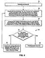
- Fig. 9 is a flow diagram illustrating a method 90 for setting a floating gate that may be implemented during a set mode, for instance, by circuits 30 and 40 of Fig. 4B.
- Figs. 10-12 illustrate voltage waveforms for Vout, Vp1, Vefb (circuit 40), Vfgr and Vfg1, for the specific implementation of method 90 discussed below relative to those figures.
- Vfg1 may be set to any voltage in order to set Vfgr during the set mode.
- Vfg1 is set to 4V during the set mode.
- Vin 4.00V
- Vcc +5V
- HV+ is about 22V
- Ip ⁇ , 12 and I2r are each about 6nA
- Ipr is about 12nA
- It ⁇ and Itr are each about 5nA
- Ig ⁇ and Igr are each about 20nA.
- circuits 30 and 40 are powered up at the beginning of the set mode, which is illustrated in Figs. 6-8 and Figs. 10-12 as time to.
- Circuit 30 at some point thereafter receives an input set voltage, e.g., Vset ⁇ , and the Vx signal from circuit 30 is received at node 27 into the gate of transistor T15 in circuit 40.
- Vcc is set to +5V
- HV+ is ramped up to a high positive voltage of about +22V, which turns on current sources 12 and I2r.
- charge pumps Ip ⁇ and Ipr are turned on to enable these current sources to begin generating their corresponding currents.
- circuit 40 can set Vfgr to within about 0.5 mV of Vfg1 in about 30 mSec, as illustrated in Figs. 10-12.
- circuit 40 causes tunnel devices Ter, Tpr, Te1 and Tp1 to operate in a dual conduction mode under the control of the voltage differential between the corresponding floating-gate erase and program electrodes for modifying the charge level on floating gates fgr and fg1. Dual conduction occurs when tunnel current flows through these four tunnel devices. Tunnel current flows through both Ter and Tpr when the voltage differential (Vefb-Vp1) is at least two tunnel voltages or approximately 22V as discussed earlier, and tunnel current flows through Te1 and Tp1 when the voltage differential (Vx-Vp1) is at least two tunnel voltages.
- circuit 40 causes dual conduction in the following manner.
- Current sources I2 and I2r are turned on and start to pull up Vx (node 12) and Vefb (node 25) respectively. For example, Vefb ramps up to about 18 volts in less than 0.5 mSec.
- the negative current sources Ip ⁇ and Ipr are turned on and pull Vp (node 3) and Vp1 (node 16) negative.
- charge pump Ip ⁇ gradually ramps Vp down to about -11V voltage in about 2 mSec
- charge pump Ipr gradually ramps Vp1 down to about -11V voltage in about 2 mSec.
- Current source Ip ⁇ controls the tunnel current that flows through tunneling devices Tp ⁇ and Te ⁇ in circuit 30, and current source Ipr controls the tunnel current that flows through tunneling devices Ter, Tpr, Te1 and Tp1 in circuit 40.
- Circuit 30 produces a Vx signal controlled by feedback from circuit 320 as described earlier.
- Vx (node 27) turns on transistor T15, which pulls up Vel (node 28) to one Vt below Vefb.
- Vel (node 28) to one Vt below Vefb.
- Vp1 ramps down to the point where the difference between Vp1 and Vel is 2 tunnel voltages, tunnel current flows through tunneling devices Te1 and Tp1. Once tunnel current is flowing in Te1 and Tp1, the voltage on floating gate fg1 (node 14) is controlled directly by Vx and to first order tracks the voltage on floating gate fg ⁇ in circuit 30 for the rest of the set mode.
- Circuit 40 produces a Vefb signal controlled by feedback from circuit 430 in a manner analogous to circuit 30.
- Vefb (node 25) turns on transistor T13, which pulls up Ver (node 17) to one Vt below Vefb.
- Vp1 node 16
- Vp1 node 16
- Vpr tunnel current flows through tunneling devices Ter and Tpr
- the voltage on fgr node 15
- I2r continues to pull up Vefb until Vefb reaches Vout + 1TV + 1Vt, where 1TV is the tunnel voltage across tunnel device TF1 and 1Vt is the threshold voltage of transistor T14.
- circuit 40 compares Vfgr with Vfg1 and generates an output voltage Vout that is a function of the difference between Vfgr and Vfg1. Circuit 40 then, at step 95, causes the voltage differential between Vefb and Vp1 to be modified as a function of Vout, and circuit 40 repeats steps 92 through 95 until circuit 40 settles to a steady state condition, at step 94 where Vfgr is approximately equal to Vfg1. At this point circuit 40 is powered down, at step 96. As a result of method 90, floating gates fgr and fg1 are each set to a charge level that will remain essentially the same over time.
- the voltage waveforms of Figs. 10-12 illustrate how circuit 40 functions during steps 92 through 95.
- Dual conduction of tunnel devices Te1 and Tp1 occurs after about 0.5 mSec, as best seen in Fig. 10.
- Vfg1 Prior to this time, Vfg1 is zero volts.
- Vfg1 is controlled by and oscillates with Vx from circuit 30, and Vfg1 tracks Vfg ⁇ .
- Dual conduction of tunnel devices Ter and Tpr occurs slightly later at about 1.5 mSec, which is illustrated as t 1 in Figs. 10-12.
- circuit 430 senses that Vfgr is not equal to Vfg1; Vout is a function of the difference between Vfgr and Vfg1; Vefb follows Vout; and Vfgr follows Vefb.
- Vfgr oscillates as Vefb moves up and down as a function of the negative feedback loop.
- the negative feedback loop causes the differential and gain stages 432 and 434, respectively, to settle to a steady state condition, where circuit 430 ceases to oscillate except for about 30mV of noise coupled to circuit 430 from the charge pump Ipr as best shown in Figs. 11 and 12 beginning at time t 2 .
- current source Igr in the gain stage 434 produces a current that is much larger than that generated by current source I2r. Therefore, the gain stage 434 is able to control Vout by sinking all the current from current source I2r that flows through T14 and TF1 to Vout.
- the compensation capacitor C3 in the gain stage 434 is made large enough to assure that the feedback loop is stable and settles in less than about 1 mSec.
- the level shift in Vetb caused by the Vt across transistor T14 approximately matches the voltage drop in T13.
- Vfgr the level shift in Vefb caused by the tunnel voltage across tunnel device TF 1 approximately matches the voltage drop across tunnel device Ter, so that when the differential and gain stages settle, Vfgr, Vfg1 and Vout are about the same. This can be seen in Fig. 12 where Vout settles to about 3.7V beginning at time t 2 , reflecting about 30 mV of noise coupled to floating gates fgr and fg1 from current source Ipr.
- circuit 40 is powered down at step 96. Powering down circuit 40 ramps down the voltages at the erase and programming electrodes toward ground, as seen beginning at time t 3 in Figs. 10-12. Step 96 may be performed by simply concurrently shutting off all of the current and voltage sources in circuits 30 and 40 at time t 3 . However, this may significantly impact Vfgr once Vefb and Vp1 have ramped back to ⁇ V. As explained above, noise from charge pump Ipr limits the accuracy of setting Vfgr equal to Vfg1 when the negative charge pump that generates Vp1 is ON.
- Vfgr may not be equal to Vfg1 at the beginning of the ramping of Vefb and Vp1 to ground. If Vfgr is not equal to Vfg1 when this ramp down begins, then Vfgr will not equal Vfg1 after Vp1 and Vefb reach ⁇ V. Moreover, during the ramp down, the current that continues to flow through tunnel devices Te1 and Tp1 and through Ter and Tpr is typically not the same. This further affects the final charge level on floating gates fgr and fg1.
- the current in the erase and program tunnel devices must be the same during this time.
- the voltage across each of the tunnel devices must be the same, which means Vefb and Vx must ramp down to ⁇ V at the same rate as Vp1 ramps up to ⁇ V.
- the tunnel device characteristics must be reasonably well matched.
- circuit 40 should be powered down, at step 96, in the following preferred manner.
- tunnel current continues to flow through tunnel devices Te ⁇ and Tp ⁇ as capacitor Cp ⁇ discharges, which pulls up Vp back towards ⁇ V. This tunnel current and the capacitance due to Cp ⁇ determine the ramp rate on Vp.
- tunnel current continues to flow through tunnel devices Ter, Te1, Tpr and Tp1 as capacitor Cpr discharges, which pulls up Vp1 back towards ⁇ V. This tunnel current and the capacitance due to Cpr determine the ramp rate on Vp1.
- Vfg ⁇ is set as described previously.
- Vfg1 tracks Vfg ⁇ , assuming Vp and Vp1 track each other reasonably closely.
- Circuit 430 senses Vfg1 moving upwards and ramps Vefb down toward ⁇ V through the feedback circuit.
- Vefb ramps down and Vp1 ramps up toward ⁇ V the tunnel current in tunnel devices Ter and Tpr decrease rapidly due to the steep slope of their Fowler-Nordheim tunnel device characteristics. Since feedback response time depends directly on the current in the erase tunnel device, the feedback circuit response slows down as Vefb ramps down toward ground. As the tunnel current decreases, both the ramp rate and feedback response times slow down and Vfgr gradually moves closer to Vfg1.
- Fig. 12 shows that Vfgr has converged to within about 0.5 mV of Vfg1 for a set mode time of 30 mSec, and Vfgr may be set even more accurately with respect to Vfg1 by allowing a ramp down time of greater than 30mV.
- the HV+ voltage supply, and thereby the I2r current source can be shut off, for instance at time t 4 , without affecting the charge on floating gates fgr and fg1.
- Vcc may be shut off.
- Vfgr is always slightly above Vfg1 so circuit 430 and the feedback circuit continue to ramp Vefb down. If Vfgr goes below Vfg1 and the feedback switches the direction Vefb is ramping, the feedback system will start to oscillate very slowly and Vfgr will diverge from Vfg1 instead of converge towards Vfg1 After Vefb and Vp1 have ramped a few volts toward ground and Vfgr is very close to Vfg1, Vefb and Vp1 can be ramped to ⁇ V quickly, as illustrated at time t 4 in Fig.
- Capacitor Cpr must be carefully set to assure that as Vp1 rises toward ground, the feedback path through the differential stage 432, gain stage 434, TF1 level shift and Ter devices to floating gate fgr is able to ramp down Vefb and move Vfgr closer and closer to Vfg1. If capacitor Cpr is too small, Vp1 rises very quickly, the delay through the feedback path causes Vefb to ramp down too slowly, and Vfgr will rise above Vfg1 instead of converging towards Vfg1.
- Cpr is designed such that the feedback response time is slightly slower than the discharge rate of Cpr.
- Cpr should be set at about 2.4pf.
- floating gates fgr and fg1 will continue to indefinitely store the charge level programmed on them during the set mode, subject to possible charge loss, e.g., due to detrapping of electrons or dielectric relaxation over time, without any external power being supplied to circuit 40.
- Vfgr was set to be approximately equal to Vfg1 those of ordinary skill in the art will realize that in another embodiment of the present invention, circuit 40 can be configured such that Vfgr is set a voltage that is some other function of Vfg1.
- circuit 30 may be configured during a read mode as a voltage reference circuit or as a comparator circuit with a built-in voltage reference.
- circuit 40 may be configured during a read mode as a voltage reference circuit or a comparator circuit with a built-in voltage reference. When circuit 40 is configured as a voltage reference, it provides a more accurate reference voltage at node 19 over that provided by circuit 30 when circuit 30 is configured as a voltage reference.
Landscapes
- Non-Volatile Memory (AREA)
- Logic Circuits (AREA)
- Control Of Electrical Variables (AREA)
- Semiconductor Integrated Circuits (AREA)
- Read Only Memory (AREA)
- Manipulation Of Pulses (AREA)
- Techniques For Improving Reliability Of Storages (AREA)
- Electronic Switches (AREA)
Claims (34)
- Un circuit à grille flottante (40) comprenant :a) une première grille flottante (fgr) pour stocker une charge là-dessus ;b) un premier condensateur de guidage (Cfgr) couplé à ladite première grille flottante (fgr) pour commander le niveau de charge sur ladite première grille flottante (fgr) comme une fonction d'une tension de consigne d'entrée (Vset) qui est couplée à travers ledit premier condensateur de guidage (Cfgr) à ladite première grille flottante (fgr) pendant un mode de réglage ;c) une seconde grille flottante (fg1) pour stocker une charge là-dessus ;d) un premier circuit (420) couplé à ladite seconde grille flottante (fg1) pour commander le niveau de charge sur ladite seconde grille flottante (fg1) pendant ledit mode de réglage ; ete) un circuit de réaction couplé entre ladite seconde grille flottante (fg1) et ladite première grille flottante (fgr) pour amener le niveau de charge au niveau de ladite première grille (fgr) à être modifié pendant ledit mode de réglage jusqu'à ce que la tension sur ladite première grille flottante (fgr) soit une fonction prédéterminée de la tension sur ladite seconde grille flottante (fg1) et de sorte qu'à la conclusion dudit mode de réglage la différence en niveau de charge entre lesdites première (fgr) et seconde grilles flottantes (fg1) soit une fonction prédéterminée de ladite tension de consigne d'entrée (Vset).
- Le circuit à grille flottante (40) de la revendication 1, où ledit circuit à grille flottante (40) atteint un état de sorte que la tension sur ladite première grille flottante (fgr) est approximativement égale à la tension sur ladite seconde grille flottante (fg1).
- Le circuit à grille flottante (40) de la revendication 1, ledit premier circuit (420) comprenant :un premier dispositif tunnel (Te1) formé entre ladite seconde grille flottante (fg1) et une première électrode tunnel (Ee1) et un second dispositif tunnel (Tp1) formé entre ladite seconde grille flottante (fg1) et une seconde électrode tunnel (Ep1) pour amener des w seconde grille flottante (fg1) comme une fonction d'un différentiel de tension entre lesdites première (Ee1) et seconde électrodes tunnels (Ep1) ;un second circuit couplé à ladite première électrode tunnel (Ee1) pour générer une première tension au niveau de ladite première électrode tunnel (Ee1) pendant ledit mode de réglage ; etun troisième circuit couplé à ladite seconde électrode tunnel (Ep1) pour générer un premier courant au niveau de ladite seconde électrode tunnel (Ep1) pendant ledit mode de réglage.
- Le circuit à grille flottante (40) de la revendication 3, où ladite seconde grille flottante (fg1) est couplée de manière capacitive à une référence de terre stable.
- Le circuit à grille flottante (40) de la revendication 3, où ledit second circuit inclut une troisième grille flottante (fg0) ayant une tension prédéterminée là-dessus pour générer une première tension.
- Le circuit à grille flottante (40) de la revendication 5, où durant ledit mode de réglage ledit circuit à grille flottante (40) atteint un état de sorte que les tensions sur lesdites première (fgr), seconde (fg1) et troisième (fg0) grille flottante sont approximativement égales.
- Le circuit à grille flottante (40) de la revendication 3 où ledit troisième circuit comprend une source de courant (Ipr) couplée entre ladite seconde électrode tunnel (Ep1) et la terre (g1).
- Le circuit à grille flottante (40) de la revendication 7 où ladite source de courant (Ipr) est une pompe de charge.
- Le circuit à grille flottante (40) de la revendication 1 comprenant de plus :un premier dispositif tunnel (Ter) formé entre ladite première grille flottante (fgr) et une première électrode tunnel (Eer) et un second dispositif tunnel (Tpr) formé entre ladite première grille flottante (fgr) et une seconde électrode tunnel (Epr) pour amener des électrons à tunneler sur et de ladite première grille flottante (fgr) pour modifier le niveau de charge sur ladite première grille flottante (fgr) comme une fonction d'un différentiel de tension entre lesdites première (Eer) et seconde électrodes tunnels (Epr), ledit premier dispositif tunnel (Ter) étant de plus inclu dans ledit circuit de réaction ; un second circuit couplé à ladite première électrode tunnel (Eer) pour générer une première tension au niveau de ladite première électrode tunnel (Eer) au début dudit mode de réglage ; etun troisième circuit couplé à ladite seconde électrode tunnel (Epr) pour générer un premier courant au niveau de ladite seconde électrode tunnel (Epr) pendant ledit mode de réglage.
- Le circuit à grille flottante (40) de la revendication 9 où
ledit second circuit comprend une première source de tension couplée entre ladite première électrode tunnel (Eer) et une source de haute tension (HV+) ; et
ledit troisième circuit comprend une première source de courant (Ipr) couplée entre ladite seconde électrode tunnel (Epr) et la terre (g1). - Le circuit à grille flottante (40) de la revendication 9, où ledit premier dispositif tunnel (Ter) est un dispositif tunnel d'effacement.
- Le circuit à grille flottante (40) de la revendication 9 où ledit second dispositif tunnel (Tpr) est un dispositif tunnel de programmation.
- Le circuit à grille flottante (40) de la revendication 9, où ledit circuit de réaction (430) comprend un étage différentiel (432) comprenant un premier (T8), second (T9), troisième (T10) et quatrième (T11) transistor, chacun desdits transistors ayant une grille et une première et seconde borne, où ladite première grille flottante (fgr) est la grille dudit premier transistor (T8), ladite second grille flottante (fg1) est la grille dudit second transistor (T9), les premières bornes desdits premier (T8) et second (T9) transistors sont couplées ensemble, les secondes bornes desdits premier (T8) et
troisième transistors (T10) sont couplées ensemble et sont de plus couplées aux grilles desdits troisième (T10) et quatrième (T11) transistors, les secondes bornes desdits second (T9) et quatrième (T11) transistors sont couplées ensemble, et les premières bornes desdits troisième (T10) et quatrième (T11) transistors sont couplées ensemble, et
un étage de gain (434) comprenant un cinquième transistor (T12) ayant une grille et une première et seconde borne, une source de courant d'étage de gain (Igr) et un condensateur de compensation (C3), où la grille dudit cinquième transistor (T12) est couplée aux secondes bornes desdits second (T9) et quatrième (T11) transistors, la première borne dudit cinquième transistor (T12) est couplée aux premières bornes desdits troisième (T10) et quatrième (T11) transistors, ledit condensateur de compensation (C3) est couplée entre la grille et la seconde borne dudit cinquième transistor (T12), et la seconde borne dudit cinquième transistor (T12) est couplée à ladite source de courant d'étage de gain (Igr) et audit second circuit. - Le circuit à grille flottante (40) de la revendication 13 où lesdits premier et second transistors (T8, T9) sont des transistors NMOS, lesdits troisième et quatrième transistors (T10, T11) sont des transistors PMOS, ledit cinquième transistor (T12) est un transistor d'excursion haute PMOS, et ladite source de courant (Igr) est une charge d'excursion basse.
- Le circuit à grille flottante (40) de la revendication 13 où lesdits premier et second transistors (T8, T9) sont des transistors PMOS, lesdits troisième et quatrième transistors (T10, T11) sont des transistors NMOS, ledit cinquième transistor (T12) est un transistor d'excursion basse NMOS, et ladite source de courant (Igr) est une charge d'excursion haute.
- Le circuit à grille flottante (40) de la revendication 1 où ledit circuit à grille flottante (40) est fabriqué en utilisant des techniques de traitement CMOS.
- Le circuit à grille flottante (40) de la revendication 1 comprenant de plus un quatrième circuit (440) couplé audit premier condensateur de guidage (Cfgr) et au circuit de réaction pour amener ladite tension de consigne d'entrée (Vset) à être couplée audit premier condensateur de guidage (Cfgr) pendant ledit mode de réglage, ledit quatrième circuit (440) créant de plus une boucle de réaction entre ladite première grille flottante (fgr) et ledit second circuit pendant un mode de lecture, ladite boucle de réaction incluant ledit premier condensateur de guidage (Cfgr) où durant ledit mode de lecture ladite boucle de réaction amène ledit circuit à grille flottante (40) à atteindre un état de sorte qu'une tension de référence est générée qui est une fonction prédéterminée de ladite tension de consigne d'entrée (Vset).
- Le circuit à grille flottante (40) de la revendication 17 où ladite tension de référence est approximativement égale à ladite tension de consigne d'entrée (Vset).
- Le circuit à grille flottante (40) de la revendication 17, où ladite tension de référence est dans la limite de 10mV autour de la valeur de ladite tension de consigne d'entrée (Vset).
- Le circuit à grille flottante (40) de la revendication 17 où ladite tension de référence est de dans la limite de 2 mV autour de la valeur de ladite tension de consigne d'entrée (Vset).
- Le circuit à grille flottante (40) de la revendication 17 où ledit quatrième circuit (440) comprend un premier interrupteur (S5) couplé entre ledit premier condensateur de guidage (Cfgr) et une borne d'entrée (450) pour recevoir ladite tension de consigne d'entrée (Vset), ledit quatrième circuit (440) comprenant de plus un second interrupteur (S4) couplé entre ledit premier condensateur de guidage (Cfgr) et ledit second circuit, où durant ledit mode de réglage ledit premier interrupteur (S5) est en position ON et ledit second interrupteur (S4) est en position OFF et durant ledit mode de lecture ledit premier interrupteur (S5) est en position OFF et ledit second interrupteur (S4) est en position ON.
- Le circuit à grille flottante (40) de la revendication 1 où ledit circuit de réaction comprend un étage différentiel (432) comprenant un premier (T8), second (T9), troisième (T10) et quatrième (T11) transistor, chacun desdits transistors ayant une grille et une première et seconde borne, où ladite première grille flottante (fgr) est la grille dudit premier transistor (T8), ladite second grille flottante (fg1) est la grille dudit second transistor (T9), les premières bornes desdits premier (T8) et second (T9) transistors sont couplées ensemble, les secondes bornes desdits premier (T8) et
troisième transistors (T10) sont couplées ensemble et sont de plus couplées aux grilles desdits troisième (T10) et quatrième (T11) transistors, les secondes bornes desdits second (T9) et quatrième (T11) transistors sont couplées ensemble, et les premières bornes desdits troisième (T10) et quatrième (T11) transistors sont couplées ensemble, et
un étage de gain (434) comprenant un cinquième transistor (T12) ayant une grille et une première et seconde borne, une source de courant d'étage de gain (Igr) et un condensateur de compensation (C3), où la grille dudit cinquième transistor (T12) est couplée aux secondes bornes desdits second (T9) et quatrième (T11) transistors, la première borne dudit cinquième transistor (T12) est couplée aux premières bornes desdits troisième (T10) et quatrième (T11) transistors, ledit condensateur de compensation (C3) est couplé entre la grille et la seconde borne dudit cinquième transistor (T12), et la seconde borne dudit cinquième transistor (T12) est couplée à ladite source de courant d'étage de gain (Igr) et audit second circuit et
où le circuit à grille flottante (40) comprend de plus :un circuit de réaction couplé entre ladite première grille flottante (fgr) et la jonction de ladite source de courant (Igr) et la seconde borne dudit cinquième transistor (T12) pour amener le niveau de charge sur ladite première grille flottante (fgr) à être modifié pendant ledit mode de réglage jusqu'à ce que le circuit à grille flottante (40) atteigne un état stationnaire de sorte que la tension sur ladite première grille flottante (fgr) soit une fonction prédéterminée de la tension sur ladite seconde grille flottante (fg1) et de sorte qu'à la conclusion dudit mode de réglage la différence en niveau de charge entre lesdites première (fgr) et seconde (fg1) grilles flottantes soit une fonction prédéterminée de ladite tension de consigne d'entrée (Vset). - Le circuit à grille flottante (40) de la revendication 1 comprenant de plus :un premier dispositif tunnel (Ter) formé entre ladite première grille flottante (fgr) et une première électrode tunnel (Eer) et un second dispositif tunnel (Tpr) formé entre ladite première grille flottante (fgr) et une seconde électrode tunnel (Epr) pour amener des électrons à tunneler sur et de ladite première grille flottante (fgr) pour modifier le niveau de charge sur ladite première grille flottante (fgr) pendant un mode de réglage comme une fonction d'un différentiel de tension entre ladite première (Eer) et seconde électrode tunnel (Epr) ; un troisième dispositif tunnel (Te1) formé entre ladite seconde grille flottante (fg1) et une troisième électrode tunnel (Ee1) et un quatrième dispositif tunnel (Tp1) formé entre ladite seconde grille flottante (fg1) et une quatrième électrode tunnel (Ep1) pour amener les électrons à tunneler sur et de ladite seconde grille flottante (fg1) ou modifier le niveau de charge sur ladite seconde grille flottante (fg1) comme une fonction d'un différentiel de tension entre lesdites troisième (Ee1) etquatrième électrodes (Ep1) ;où ledit circuit de réaction qui est couplé entre lesdites premières (fgr) et seconde (fg1) grilles flottantes comprend de plus
un étage différentiel (432) comprenant un premier (T8), second (T9), troisième (T10) et quatrième (T11) transistor, chacun desdits transistors ayant une grille et une première et seconde borne, où ladite première grille flottante (fgr) est la grille dudit premier transistor (T8), ladite second grille flottante (fg1) est la grille dudit second transistor (T9), les premières bornes desdits premier (T8) et second (T9) transistors sont couplées ensemble, les secondes bornes desdits premier (T8) et troisième transistors (T10) sont couplées ensemble et sont de plus couplées aux grilles desdits troisième (T10) et quatrième (T11) transistors, les secondes bornes desdits second (T9) et quatrième (T11) transistors sont couplées ensemble, et les premières bornes desdits troisième (T10) et quatrième (T11) transistors sont couplées ensemble, et
un étage de gain (434) comprenant un cinquième transistor (T12) ayant une grille et
une première et seconde borne, une source de courant d'étage de gain (Igr) et un condensateur de compensation (C3), où la grille dudit cinquième transistor (T12) est couplée aux secondes bornes desdits second (T9) et quatrième (T11) transistors, la première borne dudit cinquième transistor (T12) est couplée aux premières bornes desdits troisième (T10) et quatrième (T11) transistors, ledit condensateur de compensation (C3) est couplé entre la grille et la seconde borne dudit cinquième transistor (T12), et la seconde borne dudit cinquième transistor (T12) est couplée à ladite source de courant d'étage de gain (Igr) et audit second circuit et
ledit circuit à grille flottante (40) comprend de plus :une boucle de réaction couplée entre ladite première électrode tunnel (Eer) et la jonction de ladite source de courant (Igr) et la seconde borne dudit cinquième transistor (T12) pour amener la tension à la première électrode tunnel (Eer) à être modifiée pendant ledit mode de réglage jusqu'à ce que le circuit à grille flottante (40) atteigne un état stationnaire de sorte que la tension sur ladite première grille flottante (fgr) soit une fonction prédéterminée de la tension sur ladite seconde grille flottante (fg1) et de sorte qu'à la conclusion dudit mode de réglage la différence en niveau de charge entre lesdites première (fgr) et seconde (fg1) grilles flottantes soit une fonction prédéterminée de ladite tension de consigne d'entrée (Vset). - Le circuit à grille flottante (40) de la revendication 23 où lesdits premier (Ter), second (Tpr), troisième (Te1) et quatrième (Tp1) dispositifs tunnel sont des dispositifs tunnel Fowler Nordheim.
- Le circuit à grille flottante (40) de la revendication 24 où lesdits premier (Ter), second (Tpr), troisième (Te1) et quatrième (Tp1) dispositifs tunnel sont ainsi conçus comme un résultat de leur disposition de puces qu'ils correspondent relativement bien l'un à l'autre.
- Le circuit à grille flottante (40) de la revendication 23 où lesdits premier (Ter) et second (Tpr) dispositifs tunnel sont en conduction duale durant le mode de réglage et lesdits troisième (Te1) et quatrième (Tp1) dispositifs tunnel sont en conduction duale durant le mode de réglage.
- Un procédé pour fixer une tension de référence dans un circuit à double grille flottante, ledit procédé comprenant les étapes de :a) amener une tension de consigne d'entrée (Vset) à être de manière capacitive couplée à une première grille flottante (fgr) durant un mode de réglage pour contrôler le niveau de charge là-dessus ;b) amener une tension prédéterminée à être couplée à une seconde grille flottante (fg1) durant un mode de réglage pour contrôler le niveau de charge là-dessus ;c) amener le niveau de charge sur ladite première grille flottante (fgr) à être modifié jusqu'à ce que ledit circuit à double grille flottante atteigne un état pendant le mode de réglage de sorte que la tension sur ladite première grille flottante (fgr) soit une fonction prédéterminée de la tension sur ladite seconde grille flottante (fg1) et de sorte qu'à la conclusion dudit mode de réglage la différence en niveau de charge entre lesdites première (fgr) et seconde (fg1) grilles flottantes soit une fonction prédéterminée de ladite tension de consigne d'entrée (Vset).
- Le procédé de la revendication 27, où l'étape c) comprend les étapes de :c1) amener un premier (Ter) et un second dispositif tunnel (Tpr) couplés à ladite première grille flottante (fgr) à fonctionner dans un mode de conduction duale sous contrôle d'un différentiel de tension entre une première électrode tunnel (Eer) couplée audit premier dispositif tunnel (Ter) et une seconde électrode tunnel (Epr) couplée audit second dispositif tunnel (Tpr) pour modifier le niveau de charge sur ladite première grille flottante (fgr) durant ledit mode de réglage ;c2) amener la tension à ladite première électrode tunnel (Eer) à être modifiée comme une fonction de la différence entre la tension sur ladite première (fgr) et seconde (fg1) grille flottante, et ;c3) répéter les étapes c1) à c2) jusqu'à ce que ledit circuit à double grille flottante atteigne un état stationnaire de sorte que la tension de seconde grille flottante soit une fonction prédéterminée de ladite tension de première grille flottante et pour amener une différence en niveau de charge entre lesdites première (fgr) et seconde (fg1) grilles flottantes, à la conclusion dudit mode de réglage, qui est une fonction prédéterminée de ladite tension de consigne d'entrée (Vset).
- Le procédé de la revendication 28 où en étape c1) un pompe de charge est utilisée pour générer une source de courant (Igr) pour ladite opération de conduction duale desdits premier (Ter) et second (Tpr) dispositifs tunnel.
- Le procédé de la revendication 29 comprenant de plus l'étape de :d) amener ladite source de courant (Igr) à diminuer à la fin dudit mode de réglage de sorte que la tension à ladite première électrode tunnel (Eer) diminue comme une fonction de celle-ci jusqu'à ce que les deux dispositifs tunnel (Ter, Tpr) ne soient plus conducteurs.
- Le procédé de la revendication 30 où les tensions auxdites première (Eer) et seconde (Epr) électrodes tunnel sont chacune réduites à 0 Volt à la fin du mode de réglage.
- Le procédé de la revendication 30 où l'étape d) comprend de plus : amener ladite pompe de charge à diminuer en contrôlant la tension sur ladite première électrode tunnel (Eer) de sorte que la première tension de grille flottante diminue à une tension prédéterminée.
- Le procédé de la revendication 30 où l'étape b) comprend de plus : amener un troisième (Te1) et quatrième (Tp1) dispositif tunnel couplés à ladite seconde grille flottante (fg1) à fonctionner dans un mode de conduction duale sous contrôle d'un différentiel de tension entre une troisième électrode tunnel (Ee1) couplée audit troisième dispositif tunnel (Te1) et une quatrième électrode tunnel (Ep1) couplée audit quatrième dispositif tunnel (Tp1) pour contrôler la tension sur ladite seconde grille flottante (fg1).
- Le procédé de la revendication 28 comprenant de plus l'étape de :d) amener la tension à ladite première électrode tunnel (Eer) et la tension à ladite seconde électrode tunnel (Epr) à diminuer vers une tension prédéterminée de sorte que lesdits premier (Ter) et second (Tpr) dispositifs tunnels ne soient plus en conduction duale.
Applications Claiming Priority (3)
| Application Number | Priority Date | Filing Date | Title |
|---|---|---|---|
| US10/338,189 US6898123B2 (en) | 2003-01-07 | 2003-01-07 | Differential dual floating gate circuit and method for programming |
| US338189 | 2003-01-07 | ||
| PCT/US2004/000318 WO2004064115A2 (fr) | 2003-01-07 | 2004-01-07 | Circuit differentiel a double grille flottante et procede de programmation |
Publications (3)
| Publication Number | Publication Date |
|---|---|
| EP1588377A2 EP1588377A2 (fr) | 2005-10-26 |
| EP1588377A4 EP1588377A4 (fr) | 2006-04-05 |
| EP1588377B1 true EP1588377B1 (fr) | 2007-12-12 |
Family
ID=32710966
Family Applications (1)
| Application Number | Title | Priority Date | Filing Date |
|---|---|---|---|
| EP04700610A Expired - Lifetime EP1588377B1 (fr) | 2003-01-07 | 2004-01-07 | Circuit differentiel a double grille flottante et procede de programmation |
Country Status (7)
| Country | Link |
|---|---|
| US (1) | US6898123B2 (fr) |
| EP (1) | EP1588377B1 (fr) |
| JP (1) | JP4865537B2 (fr) |
| CN (1) | CN1754228B (fr) |
| AT (1) | ATE381101T1 (fr) |
| DE (1) | DE602004010617D1 (fr) |
| WO (1) | WO2004064115A2 (fr) |
Families Citing this family (16)
| Publication number | Priority date | Publication date | Assignee | Title |
|---|---|---|---|---|
| US7212446B2 (en) * | 2002-09-16 | 2007-05-01 | Impinj, Inc. | Counteracting overtunneling in nonvolatile memory cells using charge extraction control |
| US7149118B2 (en) * | 2002-09-16 | 2006-12-12 | Impinj, Inc. | Method and apparatus for programming single-poly pFET-based nonvolatile memory cells |
| US7113017B2 (en) * | 2004-07-01 | 2006-09-26 | Intersil Americas Inc. | Floating gate analog voltage level shift circuit and method for producing a voltage reference that operates on a low supply voltage |
| US6870764B2 (en) * | 2003-01-21 | 2005-03-22 | Xicor Corporation | Floating gate analog voltage feedback circuit |
| US7283390B2 (en) * | 2004-04-21 | 2007-10-16 | Impinj, Inc. | Hybrid non-volatile memory |
| US8111558B2 (en) | 2004-05-05 | 2012-02-07 | Synopsys, Inc. | pFET nonvolatile memory |
| CN101061449B (zh) * | 2004-11-18 | 2010-08-11 | Nxp股份有限公司 | 参考电压电路 |
| CN1991396B (zh) * | 2005-12-30 | 2010-05-05 | 鸿富锦精密工业(深圳)有限公司 | 电压检测装置 |
| US8122307B1 (en) | 2006-08-15 | 2012-02-21 | Synopsys, Inc. | One time programmable memory test structures and methods |
| US7616501B2 (en) * | 2006-12-04 | 2009-11-10 | Semiconductor Components Industries, L.L.C. | Method for reducing charge loss in analog floating gate cell |
| US7894261B1 (en) | 2008-05-22 | 2011-02-22 | Synopsys, Inc. | PFET nonvolatile memory |
| US7773424B2 (en) * | 2008-05-23 | 2010-08-10 | Freescale Semiconductor, Inc. | Circuit for and an electronic device including a nonvolatile memory cell and a process of forming the electronic device |
| US7859911B2 (en) * | 2008-07-21 | 2010-12-28 | Triune Ip Llc | Circuit and system for programming a floating gate |
| US7944744B2 (en) * | 2009-06-30 | 2011-05-17 | Sandisk Il Ltd. | Estimating values related to discharge of charge-storing memory cells |
| US10782420B2 (en) | 2017-12-18 | 2020-09-22 | Thermo Eberline Llc | Range-extended dosimeter |
| KR102331471B1 (ko) * | 2019-08-23 | 2021-11-26 | (주)아트로닉스 | 고전력 반도체 소자 및 그의 제조 방법 |
Family Cites Families (14)
| Publication number | Priority date | Publication date | Assignee | Title |
|---|---|---|---|---|
| US4935702A (en) | 1988-12-09 | 1990-06-19 | Synaptics, Inc. | Subthreshold CMOS amplifier with offset adaptation |
| US5059920A (en) | 1988-12-09 | 1991-10-22 | Synaptics, Incorporated | CMOS amplifier with offset adaptation |
| US4980859A (en) | 1989-04-07 | 1990-12-25 | Xicor, Inc. | NOVRAM cell using two differential decouplable nonvolatile memory elements |
| US4953928A (en) | 1989-06-09 | 1990-09-04 | Synaptics Inc. | MOS device for long-term learning |
| US5095284A (en) | 1990-09-10 | 1992-03-10 | Synaptics, Incorporated | Subthreshold CMOS amplifier with wide input voltage range |
| US5166562A (en) | 1991-05-09 | 1992-11-24 | Synaptics, Incorporated | Writable analog reference voltage storage device |
| US5430670A (en) * | 1993-11-08 | 1995-07-04 | Elantec, Inc. | Differential analog memory cell and method for adjusting same |
| JP2705605B2 (ja) * | 1995-01-20 | 1998-01-28 | 日本電気株式会社 | センスアンプ回路 |
| US5875126A (en) | 1995-09-29 | 1999-02-23 | California Institute Of Technology | Autozeroing floating gate amplifier |
| US5748534A (en) * | 1996-03-26 | 1998-05-05 | Invox Technology | Feedback loop for reading threshold voltage |
| ITMI981193A1 (it) * | 1998-05-29 | 1999-11-29 | St Microelectronics Srl | Dispositivo circuitale e relativo metodo per la propgrammazione di una cella di memoria non volatile a singola tensione di |
| US6297689B1 (en) | 1999-02-03 | 2001-10-02 | National Semiconductor Corporation | Low temperature coefficient low power programmable CMOS voltage reference |
| EP1058270B1 (fr) * | 1999-06-04 | 2007-03-21 | STMicroelectronics S.r.l. | Etage de polarisation pour la polarisation du drain d'une cellule de mémoire non-volatile pendant la lecture |
| JP3933817B2 (ja) * | 1999-06-24 | 2007-06-20 | 富士通株式会社 | 不揮発性メモリ回路 |
-
2003
- 2003-01-07 US US10/338,189 patent/US6898123B2/en not_active Expired - Fee Related
-
2004
- 2004-01-07 JP JP2006500827A patent/JP4865537B2/ja not_active Expired - Fee Related
- 2004-01-07 EP EP04700610A patent/EP1588377B1/fr not_active Expired - Lifetime
- 2004-01-07 AT AT04700610T patent/ATE381101T1/de not_active IP Right Cessation
- 2004-01-07 DE DE602004010617T patent/DE602004010617D1/de not_active Expired - Lifetime
- 2004-01-07 CN CN2004800048293A patent/CN1754228B/zh not_active Expired - Fee Related
- 2004-01-07 WO PCT/US2004/000318 patent/WO2004064115A2/fr not_active Ceased
Also Published As
| Publication number | Publication date |
|---|---|
| US6898123B2 (en) | 2005-05-24 |
| WO2004064115A2 (fr) | 2004-07-29 |
| CN1754228A (zh) | 2006-03-29 |
| EP1588377A2 (fr) | 2005-10-26 |
| EP1588377A4 (fr) | 2006-04-05 |
| JP2006520943A (ja) | 2006-09-14 |
| DE602004010617D1 (de) | 2008-01-24 |
| WO2004064115A9 (fr) | 2004-09-02 |
| ATE381101T1 (de) | 2007-12-15 |
| US20040135619A1 (en) | 2004-07-15 |
| JP4865537B2 (ja) | 2012-02-01 |
| CN1754228B (zh) | 2010-05-05 |
| WO2004064115A3 (fr) | 2005-02-24 |
Similar Documents
| Publication | Publication Date | Title |
|---|---|---|
| US7432744B2 (en) | Comparator circuit with built-in programmable floating gate voltage reference | |
| US6894928B2 (en) | Output voltage compensating circuit and method for a floating gate reference voltage generator | |
| EP1588377B1 (fr) | Circuit differentiel a double grille flottante et procede de programmation | |
| US6914812B2 (en) | Tunnel device level shift circuit | |
| US6815983B2 (en) | Analog floating gate voltage sense during dual conduction programming | |
| EP1588374B1 (fr) | Circuit de retroaction de tension analogique a grille flottante | |
| US6829164B2 (en) | Differential floating gate circuit and method for programming | |
| US6847551B2 (en) | Apparatus for feedback using a tunnel device | |
| US6867622B2 (en) | Method and apparatus for dual conduction analog programming |
Legal Events
| Date | Code | Title | Description |
|---|---|---|---|
| PUAI | Public reference made under article 153(3) epc to a published international application that has entered the european phase |
Free format text: ORIGINAL CODE: 0009012 |
|
| 17P | Request for examination filed |
Effective date: 20050824 |
|
| AK | Designated contracting states |
Kind code of ref document: A2 Designated state(s): AT BE BG CH CY CZ DE DK EE ES FI FR GB GR HU IE IT LI LU MC NL PT RO SE SI SK TR |
|
| AX | Request for extension of the european patent |
Extension state: AL LT LV MK |
|
| A4 | Supplementary search report drawn up and despatched |
Effective date: 20060221 |
|
| DAX | Request for extension of the european patent (deleted) | ||
| GRAP | Despatch of communication of intention to grant a patent |
Free format text: ORIGINAL CODE: EPIDOSNIGR1 |
|
| GRAS | Grant fee paid |
Free format text: ORIGINAL CODE: EPIDOSNIGR3 |
|
| GRAA | (expected) grant |
Free format text: ORIGINAL CODE: 0009210 |
|
| AK | Designated contracting states |
Kind code of ref document: B1 Designated state(s): AT BE BG CH CY CZ DE DK EE ES FI FR GB GR HU IE IT LI LU MC NL PT RO SE SI SK TR |
|
| REG | Reference to a national code |
Ref country code: GB Ref legal event code: FG4D |
|
| REG | Reference to a national code |
Ref country code: CH Ref legal event code: EP |
|
| REG | Reference to a national code |
Ref country code: IE Ref legal event code: FG4D |
|
| REF | Corresponds to: |
Ref document number: 602004010617 Country of ref document: DE Date of ref document: 20080124 Kind code of ref document: P |
|
| PG25 | Lapsed in a contracting state [announced via postgrant information from national office to epo] |
Ref country code: SE Free format text: LAPSE BECAUSE OF FAILURE TO SUBMIT A TRANSLATION OF THE DESCRIPTION OR TO PAY THE FEE WITHIN THE PRESCRIBED TIME-LIMIT Effective date: 20080312 Ref country code: CH Free format text: LAPSE BECAUSE OF FAILURE TO SUBMIT A TRANSLATION OF THE DESCRIPTION OR TO PAY THE FEE WITHIN THE PRESCRIBED TIME-LIMIT Effective date: 20071212 Ref country code: LI Free format text: LAPSE BECAUSE OF FAILURE TO SUBMIT A TRANSLATION OF THE DESCRIPTION OR TO PAY THE FEE WITHIN THE PRESCRIBED TIME-LIMIT Effective date: 20071212 |
|
| PG25 | Lapsed in a contracting state [announced via postgrant information from national office to epo] |
Ref country code: SI Free format text: LAPSE BECAUSE OF FAILURE TO SUBMIT A TRANSLATION OF THE DESCRIPTION OR TO PAY THE FEE WITHIN THE PRESCRIBED TIME-LIMIT Effective date: 20071212 Ref country code: FI Free format text: LAPSE BECAUSE OF FAILURE TO SUBMIT A TRANSLATION OF THE DESCRIPTION OR TO PAY THE FEE WITHIN THE PRESCRIBED TIME-LIMIT Effective date: 20071212 Ref country code: NL Free format text: LAPSE BECAUSE OF FAILURE TO SUBMIT A TRANSLATION OF THE DESCRIPTION OR TO PAY THE FEE WITHIN THE PRESCRIBED TIME-LIMIT Effective date: 20071212 |
|
| NLV1 | Nl: lapsed or annulled due to failure to fulfill the requirements of art. 29p and 29m of the patents act | ||
| REG | Reference to a national code |
Ref country code: CH Ref legal event code: PL |
|
| PG25 | Lapsed in a contracting state [announced via postgrant information from national office to epo] |
Ref country code: AT Free format text: LAPSE BECAUSE OF FAILURE TO SUBMIT A TRANSLATION OF THE DESCRIPTION OR TO PAY THE FEE WITHIN THE PRESCRIBED TIME-LIMIT Effective date: 20071212 |
|
| PG25 | Lapsed in a contracting state [announced via postgrant information from national office to epo] |
Ref country code: CZ Free format text: LAPSE BECAUSE OF FAILURE TO SUBMIT A TRANSLATION OF THE DESCRIPTION OR TO PAY THE FEE WITHIN THE PRESCRIBED TIME-LIMIT Effective date: 20071212 Ref country code: ES Free format text: LAPSE BECAUSE OF FAILURE TO SUBMIT A TRANSLATION OF THE DESCRIPTION OR TO PAY THE FEE WITHIN THE PRESCRIBED TIME-LIMIT Effective date: 20080323 |
|
| PG25 | Lapsed in a contracting state [announced via postgrant information from national office to epo] |
Ref country code: MC Free format text: LAPSE BECAUSE OF NON-PAYMENT OF DUE FEES Effective date: 20080131 Ref country code: BE Free format text: LAPSE BECAUSE OF FAILURE TO SUBMIT A TRANSLATION OF THE DESCRIPTION OR TO PAY THE FEE WITHIN THE PRESCRIBED TIME-LIMIT Effective date: 20071212 Ref country code: SK Free format text: LAPSE BECAUSE OF FAILURE TO SUBMIT A TRANSLATION OF THE DESCRIPTION OR TO PAY THE FEE WITHIN THE PRESCRIBED TIME-LIMIT Effective date: 20071212 Ref country code: RO Free format text: LAPSE BECAUSE OF FAILURE TO SUBMIT A TRANSLATION OF THE DESCRIPTION OR TO PAY THE FEE WITHIN THE PRESCRIBED TIME-LIMIT Effective date: 20071212 |
|
| EN | Fr: translation not filed | ||
| PG25 | Lapsed in a contracting state [announced via postgrant information from national office to epo] |
Ref country code: PT Free format text: LAPSE BECAUSE OF FAILURE TO SUBMIT A TRANSLATION OF THE DESCRIPTION OR TO PAY THE FEE WITHIN THE PRESCRIBED TIME-LIMIT Effective date: 20080512 |
|
| PLBE | No opposition filed within time limit |
Free format text: ORIGINAL CODE: 0009261 |
|
| STAA | Information on the status of an ep patent application or granted ep patent |
Free format text: STATUS: NO OPPOSITION FILED WITHIN TIME LIMIT |
|
| PG25 | Lapsed in a contracting state [announced via postgrant information from national office to epo] |
Ref country code: DK Free format text: LAPSE BECAUSE OF FAILURE TO SUBMIT A TRANSLATION OF THE DESCRIPTION OR TO PAY THE FEE WITHIN THE PRESCRIBED TIME-LIMIT Effective date: 20071212 Ref country code: FR Free format text: LAPSE BECAUSE OF FAILURE TO SUBMIT A TRANSLATION OF THE DESCRIPTION OR TO PAY THE FEE WITHIN THE PRESCRIBED TIME-LIMIT Effective date: 20080926 Ref country code: DE Free format text: LAPSE BECAUSE OF FAILURE TO SUBMIT A TRANSLATION OF THE DESCRIPTION OR TO PAY THE FEE WITHIN THE PRESCRIBED TIME-LIMIT Effective date: 20080313 |
|
| 26N | No opposition filed |
Effective date: 20080915 |
|
| GBPC | Gb: european patent ceased through non-payment of renewal fee |
Effective date: 20080312 |
|
| PG25 | Lapsed in a contracting state [announced via postgrant information from national office to epo] |
Ref country code: GR Free format text: LAPSE BECAUSE OF FAILURE TO SUBMIT A TRANSLATION OF THE DESCRIPTION OR TO PAY THE FEE WITHIN THE PRESCRIBED TIME-LIMIT Effective date: 20080313 Ref country code: IE Free format text: LAPSE BECAUSE OF NON-PAYMENT OF DUE FEES Effective date: 20080107 Ref country code: EE Free format text: LAPSE BECAUSE OF FAILURE TO SUBMIT A TRANSLATION OF THE DESCRIPTION OR TO PAY THE FEE WITHIN THE PRESCRIBED TIME-LIMIT Effective date: 20071212 |
|
| PG25 | Lapsed in a contracting state [announced via postgrant information from national office to epo] |
Ref country code: BG Free format text: LAPSE BECAUSE OF FAILURE TO SUBMIT A TRANSLATION OF THE DESCRIPTION OR TO PAY THE FEE WITHIN THE PRESCRIBED TIME-LIMIT Effective date: 20080312 |
|
| PG25 | Lapsed in a contracting state [announced via postgrant information from national office to epo] |
Ref country code: GB Free format text: LAPSE BECAUSE OF NON-PAYMENT OF DUE FEES Effective date: 20080312 |
|
| PG25 | Lapsed in a contracting state [announced via postgrant information from national office to epo] |
Ref country code: CY Free format text: LAPSE BECAUSE OF FAILURE TO SUBMIT A TRANSLATION OF THE DESCRIPTION OR TO PAY THE FEE WITHIN THE PRESCRIBED TIME-LIMIT Effective date: 20071212 |
|
| PG25 | Lapsed in a contracting state [announced via postgrant information from national office to epo] |
Ref country code: LU Free format text: LAPSE BECAUSE OF NON-PAYMENT OF DUE FEES Effective date: 20080107 Ref country code: HU Free format text: LAPSE BECAUSE OF FAILURE TO SUBMIT A TRANSLATION OF THE DESCRIPTION OR TO PAY THE FEE WITHIN THE PRESCRIBED TIME-LIMIT Effective date: 20080613 |
|
| PG25 | Lapsed in a contracting state [announced via postgrant information from national office to epo] |
Ref country code: TR Free format text: LAPSE BECAUSE OF FAILURE TO SUBMIT A TRANSLATION OF THE DESCRIPTION OR TO PAY THE FEE WITHIN THE PRESCRIBED TIME-LIMIT Effective date: 20071212 |
|
| PG25 | Lapsed in a contracting state [announced via postgrant information from national office to epo] |
Ref country code: IT Free format text: LAPSE BECAUSE OF NON-PAYMENT OF DUE FEES Effective date: 20080131 |