EP1589514A2 - Circuit de traitement de signaux vidéo, dispositif d'affichage vidéo, et dispositif de commande d'affichage - Google Patents
Circuit de traitement de signaux vidéo, dispositif d'affichage vidéo, et dispositif de commande d'affichage Download PDFInfo
- Publication number
- EP1589514A2 EP1589514A2 EP05252464A EP05252464A EP1589514A2 EP 1589514 A2 EP1589514 A2 EP 1589514A2 EP 05252464 A EP05252464 A EP 05252464A EP 05252464 A EP05252464 A EP 05252464A EP 1589514 A2 EP1589514 A2 EP 1589514A2
- Authority
- EP
- European Patent Office
- Prior art keywords
- video signal
- line
- lines
- video
- display
- Prior art date
- Legal status (The legal status is an assumption and is not a legal conclusion. Google has not performed a legal analysis and makes no representation as to the accuracy of the status listed.)
- Withdrawn
Links
- 239000004973 liquid crystal related substance Substances 0.000 claims abstract description 23
- 238000006243 chemical reaction Methods 0.000 claims abstract description 18
- 238000000034 method Methods 0.000 claims description 15
- 230000006866 deterioration Effects 0.000 abstract description 6
- 238000009877 rendering Methods 0.000 abstract description 3
- 238000010586 diagram Methods 0.000 description 18
- 230000003111 delayed effect Effects 0.000 description 2
- 230000006870 function Effects 0.000 description 2
- 238000012935 Averaging Methods 0.000 description 1
- 230000005540 biological transmission Effects 0.000 description 1
- 230000003247 decreasing effect Effects 0.000 description 1
- 230000000694 effects Effects 0.000 description 1
- 230000000750 progressive effect Effects 0.000 description 1
Images




Classifications
-
- G—PHYSICS
- G09—EDUCATION; CRYPTOGRAPHY; DISPLAY; ADVERTISING; SEALS
- G09G—ARRANGEMENTS OR CIRCUITS FOR CONTROL OF INDICATING DEVICES USING STATIC MEANS TO PRESENT VARIABLE INFORMATION
- G09G3/00—Control arrangements or circuits, of interest only in connection with visual indicators other than cathode-ray tubes
- G09G3/20—Control arrangements or circuits, of interest only in connection with visual indicators other than cathode-ray tubes for presentation of an assembly of a number of characters, e.g. a page, by composing the assembly by combination of individual elements arranged in a matrix no fixed position being assigned to or needed to be assigned to the individual characters or partial characters
- G09G3/2092—Details of a display terminals using a flat panel, the details relating to the control arrangement of the display terminal and to the interfaces thereto
-
- G—PHYSICS
- G09—EDUCATION; CRYPTOGRAPHY; DISPLAY; ADVERTISING; SEALS
- G09G—ARRANGEMENTS OR CIRCUITS FOR CONTROL OF INDICATING DEVICES USING STATIC MEANS TO PRESENT VARIABLE INFORMATION
- G09G2310/00—Command of the display device
- G09G2310/02—Addressing, scanning or driving the display screen or processing steps related thereto
- G09G2310/0202—Addressing of scan or signal lines
- G09G2310/0205—Simultaneous scanning of several lines in flat panels
- G09G2310/021—Double addressing, i.e. scanning two or more lines, e.g. lines 2 and 3; 4 and 5, at a time in a first field, followed by scanning two or more lines in another combination, e.g. lines 1 and 2; 3 and 4, in a second field
-
- G—PHYSICS
- G09—EDUCATION; CRYPTOGRAPHY; DISPLAY; ADVERTISING; SEALS
- G09G—ARRANGEMENTS OR CIRCUITS FOR CONTROL OF INDICATING DEVICES USING STATIC MEANS TO PRESENT VARIABLE INFORMATION
- G09G2340/00—Aspects of display data processing
- G09G2340/04—Changes in size, position or resolution of an image
- G09G2340/0407—Resolution change, inclusive of the use of different resolutions for different screen areas
- G09G2340/0414—Vertical resolution change
-
- G—PHYSICS
- G09—EDUCATION; CRYPTOGRAPHY; DISPLAY; ADVERTISING; SEALS
- G09G—ARRANGEMENTS OR CIRCUITS FOR CONTROL OF INDICATING DEVICES USING STATIC MEANS TO PRESENT VARIABLE INFORMATION
- G09G2340/00—Aspects of display data processing
- G09G2340/04—Changes in size, position or resolution of an image
- G09G2340/0407—Resolution change, inclusive of the use of different resolutions for different screen areas
- G09G2340/0421—Horizontal resolution change
Definitions
- the present invention relates to a video signal processing circuit, a video display, and a display driving device used for applying a scale conversion to a video signal so as to drive a display, and so on.
- a resolution of a VGA panel is vertical 480 lines/horizontal 640 dots, and that of the XGA is vertical 768 lines/horizontal 1024 dots.
- a video signal there are standards such as an NTSC, a PAL, and others.
- the resolution is vertical 240 lines/horizontal 720 dots. Due to this, in a case of driving the liquid crystal panel by the video signal, it is needed to convert (apply a scale conversion to) the number of horizontal dots and the number of vertical dots of the video signal into the resolution according to the liquid crystal panel.
- a scale conversion method there is a method in which after a 480 I (interlace) signal is once up-converted to a 480 P (progressive) signal, the number of scanning lines is increased to the resolution of the panel by using a vertical-direction scaler (see Japanese Patent Application Laying-open No.H5-252486).
- a horizontal direction an ordinary interpolating filter is used so as to increase the number of horizontal dots to a predetermined panel horizontal resolution.
- a movement-adaptive sequential scanning conversion is used.
- This conversion requires a large-capacity memory, and a complicated signal processing circuit.
- a sequential scanning for averaging upper scanning-line information and lower scanning-line information is carried out, so that a preferred video is obtained in a still video.
- a moving video portion obtained is a video in which a vertical resolution is decreased to half, thus a video quality is greatly deteriorated.
- a video signal processing circuit of the present invention is a video signal processing circuit for applying a scale conversion to a video signal, and comprises a vertical scaler in which a number-of-line increasing rate ⁇ of with respect to the video signal is set to 0 ⁇ ⁇ ⁇ 2, and a reading-out circuit for reading out the same line of the video signal output from the vertical scaler for one or a plurality of times during one horizontal period.
- a video signal processing circuit of the present invention is a video signal processing circuit for applying a scale conversion to a video signal, and comprises a reading-out circuit for reading out the same line of the video signal for one or a plurality of times during one horizontal period, and a vertical scaler in which a number-of-line increasing rate ⁇ with respect to the video signal output from the reading-out circuit is set to 0 ⁇ ⁇ ⁇ 2.
- a video signal processing circuit of these configurations may have a horizontal scaler for converting the number of dots of a horizontal direction with respect to the video signal.
- the number-of-line increasing rate ⁇ of the vertical scaler may be selected within a range from about 0.66 to about 1.58.
- the video display of the present invention is provided with any one of the video signal processing circuits described above, and configured as to supply an output video signal from the video signal processing circuit to a hold-type display panel such as a liquid crystal panel, and others.
- a display driving device of the present invention is a display driving device, for applying a scale conversion to a video signal so as to drive a display, and comprises a vertical scaler in which a number-of-line increasing rate ⁇ with respect to the video signal is set to 0 ⁇ ⁇ ⁇ 2, and a timing controller for writing continuously or simultaneously the same line of a video signal output from the vertical scaler into one or a plurality of lines of a display.
- a display driving device of the above configuration may have a horizontal scaler for converting the number of dots of a horizontal direction with respect to the video signal according to the number of horizontal dots of the display.
- a number-of-line increasing rate of the vertical scaler may be selected within a range from about 0.66 to about 1.58.
- the display may be a hold-type display panel such as a liquid crystal panel, and others.
- the scale conversion it is possible to exhibit desired effects such as rendering a circuit scale small, and alleviating a deterioration of the vertical resolution.
- FIG. 1 is a block diagram showing a video display.
- This video display is formed of a video signal processing circuit 1, and a liquid crystal display panel (LCD) 2.
- the video signal processing circuit 1 is formed of a vertical scaler 11 (11A, or 11B), a number-of-a-plurality-of-time reading-out circuit 12, and a horizontal scaler 13.
- An input video signal is a digitized video signal (a video signal formed of a luminance signal and a color difference signal, or a video signal formed of an RGB signal, and so on), and input into the vertical scaler 11.
- the vertical scaler 11 is provided with a function of increasing the number of scanning lines of the input video signal. However, an increasing rate of the number of scanning lines is adjacent to 1.0.
- the number of unit output lines from the vertical scaler 11 is M
- the number of unit input lines to the vertical scaler 11 is N
- the increasing rate is ⁇
- the vertical scaler 11A shown in Figure 2, or the vertical scaler 11B shown in Figure 4 is adopted.
- the vertical scaler 11A is formed of being provided with one line memory 11a.
- Figure 3 shows an operation timing chart of the line memory 11a.
- a horizontal axis is a time period
- a vertical axis is an address value of the line memory 11a.
- Solid lines indicate write addresses
- dotted lines indicate read addresses.
- a, b, c, ⁇ in an inputting and an outputting indicates a one-line video signal.
- the vertical scaler 11B shown in Figure 4 has a circuit configuration capable of preventing the one-line video (a) from being output twice.
- the vertical scaler 11B is formed of being provided with a first line memory 11b, a second line memory 11c, a first multiplier 11d, a second multiplier 11e, and an adder 11f.
- the first line memory 11b operates similar to a case of the above-described line memory 11a.
- An output of the first line memory 11b is input into the first multiplier 11d and the second line memory 11c.
- the second line memory 11c outputs input data by delaying only by one horizontal period in a read system.
- a vertical-direction interpolating filter is constituted.
- the data delayed by the second line memory 11c is input into the second multiplier 11e.
- the first multiplier 11d multiplies the input data from the first line memory 11b by m-time and outputs the multiplied data
- the second multiplier 11e multiplies the input data from the second line memory 11c by n-time and outputs the multiplied data.
- the adder 11f inputs the m-time output data and the n-time output data, and outputs a value in which these data are added.
- Figure 5 is an operation timing chart of the vertical scaler 11B.
- a horizontal axis is a time period, and a vertical axis is an address value of the line memory. Solid lines indicate write addresses, and dotted lines indicate read addresses.
- the vertical scaler 11B does not allow the same video signal to be output for two consecutive times.
- a line memory may be further dependently connected to the final stage of the second line memory 11c.
- Figure 6 is a block diagram showing the number-of-a-plurality-of-time reading-out circuit 12.
- This number-of-a-plurality-of-time reading-out circuit 12 is formed of being provided with a third line memory 12a, a fourth line memory 12b, and a selection circuit 12c.
- the third line memory 12a and the fourth line memory 12b take turns from one line to another carrying out a writing of the video signal from the vertical scaler 11 by an input system clock (corresponds to writing clocks of the first line memory 11b and the second line memory 11c).
- a reading-out is carried out by a clock that is an integral multiple of this writing clock (one time, two times, three times, and so on, for example).
- Figure 7 is a timing chart showing a process of the number-of-a-plurality-of-time reading-out circuit 12.
- the reading-out is carried out by a 3-time clock.
- an address overtaking occurs.
- the third line memory 12a, and the fourth line memory 12b are arranged in parallel.
- the selection circuit 12c selects the same video signal read out three times from the third line memory 12a, and outputs the selected video signal.
- the selection circuit 12c switches to a side of the fourth line memory 12b, selects the same video signal read out three times from the fourth line memory 12b, and outputs the selected video signal. Furthermore, the selection circuit 12c switches to a side of the third line memory 12a once again, and repeats a similar switching process. That is, the number-of-a-plurality-of-time reading-out circuit 12 is constituted of carrying out the reading-out by the 3-time clock, and not selecting the video signal read out by the address overtaking.
- the horizontal scaler 13 inputs the video signal from the number-of-a-plurality-of-time reading-out circuit 12, and converts the number of horizontal dots of this video signal into the number of horizontal dots of the liquid crystal panel 2.
- the liquid crystal panel 2 is the XGA panel
- an input signal (720 dots) is converted into a horizontal resolution (1024 dots) of the XGA panel.
- a one-dimensional interpolating filter may be used.
- N' is the number of total input video scanning lines.
- the vertical resolution of the VGA panel is 480 lines
- a signal of which synchronization is unstable e.g., completely not conforming to the NTSC (PAL) standard
- PAL NTSC
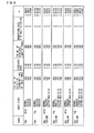
- Figure 8 is a descriptive diagram showing a relationship among resolutions of various kinds of video display panels, formats of various kinds of video signals, the number of effective scanning lines of the input video, a displayed rate, the number of displayed lines of panels, a magnifying rate K of the number-of-a-plurality-of-time reading-out circuit, and an increasing rate ⁇ .
- the increasing rate ⁇ may be selected within a range from about 0.66 to about 1.58.
- the number of scanning lines of the NTSC is 525
- the number of scanning lines of the PAL is 625 lines.
- the number of output lines from the vertical scaler is an integer (a numerator is M, and a denominator is N).
- the number of output lines from the vertical scaler is an integer.
- the number of the scanning lines being the integer, it becomes easier to create a circuit.
- the vertical scaler 11 having the increasing rate ⁇ of 0 ⁇ ⁇ ⁇ 2 (that is, ⁇ is approximate to 1.0) is used, so that it is possible to render a deterioration of a video small, and a circuit scale small. Furthermore, the number-of-a-plurality-of-time reading-out circuit 12 is used by being brought into a combination with this vertical scaler 11, it becomes possible to realize a vertical scaling process that is finally needed, and render very small the circuit scale.
- the number-of-a-plurality-of-time reading-out circuit 12 is provided at the final stage of the vertical scaler 11, this is not always the case, and an arranging relationship between the vertical scaler 11 and the number-of-a-plurality-of-time reading-out circuit 12 may be reversed.
- an example in which the liquid crystal panel is driven is shown, and however, this is not always the case.
- the video display of the present invention is capable of improving the video quality, particularly, in a case of being provided with a so-called hold-type display element such as a liquid crystal panel, and driving the element.
- FIG. 9 is a block diagram showing a display driving device 101 that drives a liquid crystal panel 115.
- the video signal to be input is a digitized video signal (a video signal formed of a luminance signal and a color difference signal, and a video signal formed of an RGB signal, and so on).
- the video signal is input into vertical scalers 111 (111A, 111B) of the display driving device 101.
- the vertical scaler 111 is provided with a function of increasing the number of scanning lines of the video signal. However, an increasing rate of the number of scanning lines is adjacent to 1.0.
- the number of unit output lines from the vertical scaler 111 is M
- the number of unit input lines to the vertical scaler 111 is N
- the increasing rate is ⁇
- the vertical scaler 111 As the vertical scaler 111, the vertical scaler 111A shown in Figure 10 or the vertical scaler 111B shown in Figure 12 is adopted. Of course, the vertical scalers are not limited thereto.
- the vertical scaler 111A is configured of being provided with one line memory 111a.
- Figure 11 shows an operation timing chart of the line memory 111a.
- a horizontal axis is a time period
- a vertical axis is an address value of the line memory 111a.
- Solid lines indicate write addresses
- dotted lines indicate read addresses.
- Each of a, b, c, ⁇ in an inputting and an outputting indicates one-line video signal.
- the vertical scaler 111 B shown in Figure 12 has a circuit configuration capable of preventing the one-line video (a) from being output twice.
- the vertical scaler 111B is formed of being provided with a first line memory 111b, a second line memory 111c, a first multiplier 111d, a second multiplier 111e, and an adder 111f.
- the first line memory 111b operates similar to a case of the above-described line memory 111a.
- An output of the first line memory 111b is input into the first multiplier 111d and the second line memory 111c.
- the second line memory 111c outputs input data by delaying only by one horizontal period in a read system.
- a vertical-direction interpolating filter is constituted.
- the data delayed by the second line memory 111c is input into the second multiplier 111e.
- the first multiplier 111d multiplies the input data from the first line memory 111b by m-time and outputs the multiplied data
- the second multiplier 111e multiplies the input data from the second line memory 111c by n-time and outputs the multiplied data.
- the adder 111 f inputs the m-time output data, and the n-time output data, and outputs a value corresponding to the sum of these data.
- Figure 13 is an operation timing chart of the vertical scaler 111B.
- a horizontal axis is a time period, and a vertical axis is an address value of the line memory. Solid lines indicate write addresses, and dotted lines indicate read addresses.
- the vertical scaler 111 B does not allow the same video signal to be output for two consecutive times.
- a line memory may be further dependently connected to the final stage of the second line memory 111c.
- the horizontal scaler 112 converts the number of horizontal dots of the video signal input from the vertical scaler 111 into the number of horizontal dots of liquid crystal panel 115.
- the liquid crystal panel 115 is an XGA panel
- the input signal (720 dots) is converted into a horizontal resolution (1024 dots) of the XGA panel.
- a one-dimensional interpolating filter may be used.
- FIG 14 is a circuit diagram showing a timing controller (hereinafter, briefly referred to as a controller) 114 capable of simultaneously writing a plurality of lines; and the liquid crystal panel 115 in a liquid crystal module 113.
- Figure 15 is a timing chart showing an operation of the above-described controller 114.
- the input signal is a digital signal formed of three data, i.e., R data, G data, and B data, each of which is 8 bits.
- R data i.e., R data, G data, and B data
- a normal video display method will be described.
- the input signal is sequentially shifted in a shift register.
- each data is fetched within a latch circuit by a latch pulse output from a timing creating circuit 114a.
- the line number selected by a gate driver line selection pulse creating circuit 114b is 0 (zero)
- the video signal that is D/A (digital and analog)-converted is written into a line 0 (zero).
- the number of lines to be selected is sequentially shifted to 1, 2, 3, and the video is displayed on the panel.
- the number of the shift registers and D/A converters is coincident with the horizontal resolution of the panel, and in a case of the XGA panel, the number of the shift registers and D/A converters is 1024. Furthermore, the number of vertical lines is 768.
- N' is the number of total input video scanning lines
- the vertical resolution of the VGA panel is 480 lines
- a signal of which synchronization is unstable e.g., completely not conforming to the NTSC (PAL) standard
- PAL NTSC
- Figure 8 shown in the embodiment 1 is adaptable in this embodiment, too.
- the vertical scaler 111 having the increasing rate ⁇ of 0 ⁇ ⁇ ⁇ 2 (that is, ⁇ is approximate to 1.0) is used, so that it is possible to render a deterioration of a video quality small, and a circuit scale small. Furthermore, the plurality-of-line simultaneous writing controller 114 is used by being brought into a combination with this vertical scaler 111, and thus, it becomes possible to realize a vertical scaling process that is finally needed, and render very small the circuit scale.
- the display driving device of the present invention is capable of improving the video quality, in particular, in a case of being provided with a so-called hold-type display element such as a liquid crystal panel, and driving the element.
- the signal processing circuits described above may be implemented by a programmable processor device receiving program instructions from a data carrier such as a memory, or provided to a memory via a data transmission link.
Landscapes
- Engineering & Computer Science (AREA)
- Physics & Mathematics (AREA)
- Computer Hardware Design (AREA)
- General Physics & Mathematics (AREA)
- Theoretical Computer Science (AREA)
- Liquid Crystal Display Device Control (AREA)
- Transforming Electric Information Into Light Information (AREA)
- Control Of Indicators Other Than Cathode Ray Tubes (AREA)
Applications Claiming Priority (4)
| Application Number | Priority Date | Filing Date | Title |
|---|---|---|---|
| JP2004128638 | 2004-04-23 | ||
| JP2004128637A JP2005311886A (ja) | 2004-04-23 | 2004-04-23 | 映像信号処理回路及び映像表示装置 |
| JP2004128637 | 2004-04-23 | ||
| JP2004128638A JP3863887B2 (ja) | 2004-04-23 | 2004-04-23 | ディスプレイ駆動装置 |
Publications (1)
| Publication Number | Publication Date |
|---|---|
| EP1589514A2 true EP1589514A2 (fr) | 2005-10-26 |
Family
ID=34940935
Family Applications (1)
| Application Number | Title | Priority Date | Filing Date |
|---|---|---|---|
| EP05252464A Withdrawn EP1589514A2 (fr) | 2004-04-23 | 2005-04-20 | Circuit de traitement de signaux vidéo, dispositif d'affichage vidéo, et dispositif de commande d'affichage |
Country Status (3)
| Country | Link |
|---|---|
| US (1) | US7408589B2 (fr) |
| EP (1) | EP1589514A2 (fr) |
| TW (1) | TWI267255B (fr) |
Families Citing this family (1)
| Publication number | Priority date | Publication date | Assignee | Title |
|---|---|---|---|---|
| TWI479893B (zh) * | 2008-09-25 | 2015-04-01 | Generalplus Technology Inc | 視訊訊號處理方法與裝置 |
Family Cites Families (11)
| Publication number | Priority date | Publication date | Assignee | Title |
|---|---|---|---|---|
| JPH05252486A (ja) | 1992-03-03 | 1993-09-28 | Hitachi Ltd | 映像信号の走査変換装置 |
| JPH06311426A (ja) | 1993-04-22 | 1994-11-04 | Olympus Optical Co Ltd | 画像処理装置 |
| JP3258773B2 (ja) | 1993-07-30 | 2002-02-18 | 三洋電機株式会社 | 多方式対応液晶表示装置 |
| JPH104529A (ja) | 1996-06-18 | 1998-01-06 | Matsushita Electric Ind Co Ltd | 画像表示装置 |
| US5781241A (en) * | 1996-11-08 | 1998-07-14 | Chrontel, Inc. | Apparatus and method to convert computer graphics signals to television video signals with vertical and horizontal scaling requiring no frame buffers |
| US6100870A (en) * | 1997-05-30 | 2000-08-08 | Texas Instruments Incorporated | Method for vertical imaging scaling |
| US6903733B1 (en) * | 1997-11-24 | 2005-06-07 | Pixelworks, Inc. | Ultra-high bandwidth multi-port memory system for image scaling applications |
| JP2000020709A (ja) | 1998-07-02 | 2000-01-21 | Pioneer Electron Corp | 映像信号処理装置 |
| JP4449102B2 (ja) | 1999-05-31 | 2010-04-14 | パナソニック株式会社 | 画像表示装置 |
| JP3837690B2 (ja) * | 1999-12-03 | 2006-10-25 | パイオニア株式会社 | 映像信号処理装置 |
| US6597402B1 (en) * | 2000-05-10 | 2003-07-22 | Sage, Inc. | Reduced television display flicker and perceived line structure with low horizontal scan rates |
-
2005
- 2005-04-08 TW TW094111109A patent/TWI267255B/zh not_active IP Right Cessation
- 2005-04-20 EP EP05252464A patent/EP1589514A2/fr not_active Withdrawn
- 2005-04-21 US US11/110,815 patent/US7408589B2/en not_active Expired - Fee Related
Also Published As
| Publication number | Publication date |
|---|---|
| TWI267255B (en) | 2006-11-21 |
| US7408589B2 (en) | 2008-08-05 |
| US20050237437A1 (en) | 2005-10-27 |
| TW200537828A (en) | 2005-11-16 |
Similar Documents
| Publication | Publication Date | Title |
|---|---|---|
| US8063861B2 (en) | Image display unit | |
| US6593939B2 (en) | Image display device and driver circuit therefor | |
| EP0735755B1 (fr) | Convertisseur universel de l'échantillonnage d'un format vidéo | |
| EP1164568A1 (fr) | Dispositif et procede de conversion de signaux video | |
| JPH1175220A (ja) | 映像信号変換器 | |
| US7602401B2 (en) | Image display apparatus and method, program therefor, and recording medium having recorded thereon the same | |
| EP1018259B1 (fr) | Filtrage du papillotement et compensation du surbalayage | |
| US8488060B2 (en) | Image signal processing apparatus for converting an interlace signal to a progressive signal | |
| EP1589514A2 (fr) | Circuit de traitement de signaux vidéo, dispositif d'affichage vidéo, et dispositif de commande d'affichage | |
| JP2004304390A (ja) | 信号処理装置 | |
| JP4483255B2 (ja) | 液晶表示装置 | |
| JPH09212131A (ja) | 画像処理装置 | |
| JP3863887B2 (ja) | ディスプレイ駆動装置 | |
| CN100409682C (zh) | 图像信号处理电路、图像显示装置和显示器驱动装置 | |
| KR19980064554A (ko) | 화상 처리 장치 및 방법 | |
| JP5045119B2 (ja) | 色トランジェント補正装置 | |
| JP2004357253A (ja) | 映像信号変換装置、映像信号処理装置及び映像表示装置 | |
| JP4392531B2 (ja) | 画像信号の処理装置および処理方法並びに画像表示装置 | |
| JP3473093B2 (ja) | 表示システム | |
| JP4608889B2 (ja) | 液晶表示装置 | |
| JP4367193B2 (ja) | 走査線変換装置 | |
| JP3895946B2 (ja) | 表示装置及びその制御回路 | |
| JP4646556B2 (ja) | ディスプレイ駆動装置 | |
| JP2000148059A (ja) | ライン数変換処理回路およびこれを搭載した表示装置 | |
| JP2008040384A (ja) | 映像信号処理システム及びこれを用いた表示装置 |
Legal Events
| Date | Code | Title | Description |
|---|---|---|---|
| PUAI | Public reference made under article 153(3) epc to a published international application that has entered the european phase |
Free format text: ORIGINAL CODE: 0009012 |
|
| AK | Designated contracting states |
Kind code of ref document: A2 Designated state(s): AT BE BG CH CY CZ DE DK EE ES FI FR GB GR HU IE IS IT LI LT LU MC NL PL PT RO SE SI SK TR |
|
| AX | Request for extension of the european patent |
Extension state: AL BA HR LV MK YU |
|
| STAA | Information on the status of an ep patent application or granted ep patent |
Free format text: STATUS: THE APPLICATION IS DEEMED TO BE WITHDRAWN |
|
| 18D | Application deemed to be withdrawn |
Effective date: 20071102 |