EP1589569A2 - Druckgiessmaschine zum Einkapseln von Halbleiterelementen und Anwendungsmethode - Google Patents
Druckgiessmaschine zum Einkapseln von Halbleiterelementen und Anwendungsmethode Download PDFInfo
- Publication number
- EP1589569A2 EP1589569A2 EP05251038A EP05251038A EP1589569A2 EP 1589569 A2 EP1589569 A2 EP 1589569A2 EP 05251038 A EP05251038 A EP 05251038A EP 05251038 A EP05251038 A EP 05251038A EP 1589569 A2 EP1589569 A2 EP 1589569A2
- Authority
- EP
- European Patent Office
- Prior art keywords
- cavity
- casting system
- injection casting
- dispensing
- mold unit
- Prior art date
- Legal status (The legal status is an assumption and is not a legal conclusion. Google has not performed a legal analysis and makes no representation as to the accuracy of the status listed.)
- Withdrawn
Links
Images


Classifications
-
- H—ELECTRICITY
- H10—SEMICONDUCTOR DEVICES; ELECTRIC SOLID-STATE DEVICES NOT OTHERWISE PROVIDED FOR
- H10P—GENERIC PROCESSES OR APPARATUS FOR THE MANUFACTURE OR TREATMENT OF DEVICES COVERED BY CLASS H10
- H10P72/00—Handling or holding of wafers, substrates or devices during manufacture or treatment thereof
- H10P72/04—Apparatus for manufacture or treatment
- H10P72/0441—Apparatus for sealing, encapsulating, glassing, decapsulating or the like
-
- A—HUMAN NECESSITIES
- A45—HAND OR TRAVELLING ARTICLES
- A45B—WALKING STICKS; UMBRELLAS; LADIES' OR LIKE FANS
- A45B25/00—Details of umbrellas
- A45B25/06—Umbrella runners
- A45B25/08—Devices for fastening or locking
-
- A—HUMAN NECESSITIES
- A45—HAND OR TRAVELLING ARTICLES
- A45B—WALKING STICKS; UMBRELLAS; LADIES' OR LIKE FANS
- A45B19/00—Special folding or telescoping of umbrellas
- A45B19/04—Special folding or telescoping of umbrellas with telescopic sticks
-
- B—PERFORMING OPERATIONS; TRANSPORTING
- B29—WORKING OF PLASTICS; WORKING OF SUBSTANCES IN A PLASTIC STATE IN GENERAL
- B29C—SHAPING OR JOINING OF PLASTICS; SHAPING OF MATERIAL IN A PLASTIC STATE, NOT OTHERWISE PROVIDED FOR; AFTER-TREATMENT OF THE SHAPED PRODUCTS, e.g. REPAIRING
- B29C39/00—Shaping by casting, i.e. introducing the moulding material into a mould or between confining surfaces without significant moulding pressure; Apparatus therefor
- B29C39/02—Shaping by casting, i.e. introducing the moulding material into a mould or between confining surfaces without significant moulding pressure; Apparatus therefor for making articles of definite length, i.e. discrete articles
- B29C39/10—Shaping by casting, i.e. introducing the moulding material into a mould or between confining surfaces without significant moulding pressure; Apparatus therefor for making articles of definite length, i.e. discrete articles incorporating preformed parts or layers, e.g. casting around inserts or for coating articles
-
- B—PERFORMING OPERATIONS; TRANSPORTING
- B29—WORKING OF PLASTICS; WORKING OF SUBSTANCES IN A PLASTIC STATE IN GENERAL
- B29D—PRODUCING PARTICULAR ARTICLES FROM PLASTICS OR FROM SUBSTANCES IN A PLASTIC STATE
- B29D11/00—Producing optical elements, e.g. lenses or prisms
- B29D11/00009—Production of simple or compound lenses
- B29D11/00278—Lenticular sheets
- B29D11/00298—Producing lens arrays
-
- H—ELECTRICITY
- H10—SEMICONDUCTOR DEVICES; ELECTRIC SOLID-STATE DEVICES NOT OTHERWISE PROVIDED FOR
- H10W—GENERIC PACKAGES, INTERCONNECTIONS, CONNECTORS OR OTHER CONSTRUCTIONAL DETAILS OF DEVICES COVERED BY CLASS H10
- H10W74/00—Encapsulations, e.g. protective coatings
- H10W74/01—Manufacture or treatment
- H10W74/016—Manufacture or treatment using moulds
Definitions
- the present invention generally concerns encapsulating semiconductor devices and specifically an injection casting system for encapsulating semiconductor devices.
- Encapsulating semiconductors is an important step for protecting a semiconductor surface such as a printed circuit board (PCB) from degrading.
- encapsulating permits the forming of lens for use with Infrared Data Transceivers (IrDT) while still protecting the PCB.
- IrDT Infrared Data Transceivers
- IrDT as a device to transmit and receive data wirelessly has been gaining popularity.
- Devices are equipped with infrared modules such as personal digital assistants (PDA), notebook/laptop computers, digital cameras, mobile phones, and many more.
- PDA personal digital assistants
- notebook/laptop computers digital cameras
- mobile phones and many more.
- an objective of the present invention is the ability to incorporate PCBs into the injection casting system.
- a cast process is extensively used in the encapsulation process.
- the cast process is especially economical for low volume production and research and development (R&D) work when compared to a transfer mold.
- R&D research and development
- Transfer molding onto PCB substrates with an unfilled epoxy also presents more challenges than transfer molding onto leadframes substrates.
- a further objective of the present invention is to integrate the advantages of the cast process including simplicity, low cost, and fast turn around time.
- the current cast process uses room temperature vulcanizing (RTV) silicone as the mold material.
- RTV silicone comes in two parts which are then mixed and cured in a master mold to form the epoxy casting RTV silicone molds.
- the resulting RTV silicone molds are then used to encapsulate the semiconductor substrates.
- the RTV silicone molds are problematic because they wear out fast and normally last for 10 to 20 cast cycles after which new molds will have to be made again.
- the RTV silicone mold's properties depend on mix ratio and cure temperature and are therefore susceptible to unintended variations.
- the use of molds using silicone are problematic because silicone absorbs moisture which can create problematic air bubbles. Silicone is not the best processing agent either because of long preheat and cure time because silicone has poor thermal conductivity. Therefore, a further objective of the present invention is to avoid the problems associated with RTV silicone molds, minimize mold wear, minimize water and air absorption , and provide for shorter preheat and cure times.
- each cavity may have lens aperture which would also have to be individually filled.
- This process is manual and requires a long cycle time.
- the yield varies depending on the operator's skill.
- An automatic solution for this process is difficult to achieve because of the individual manipulation of epoxy for each cavity and lens aperture. Therefore, a still further objective of the present invention is the provision of a fast, simple and easy process that shortens cycle time and improves yield.
- a still further objective of the present invention is the use of a vacuum or pressurized chamber to eliminate air bubbles.
- RTV silicone molds are several other problems.
- the substrate or PCB size is limited due to a large thermal expansion mismatch between silicone RTV and PCB substrates and the narrow processing (i.e. curing) temperature for RTV silicone molds. Therefore, a still further objective of the present invention is to minimize the expansion mismatch and the narrow processing temperature associated with RTV silicone molds.
- a still further objective of the present invention is the provision of a injection casting system for encapsulating semiconductor devices and method of use that is economical to manufacture, durable in use, and efficient in operation.
- An injection casting system for encapsulating semiconductor devices and method of use has been developed to improve yield, to reduce encapsulation time, and to allow encapsulating deep lens cavity for optoelectronic devices.
- This invention utilizes a combination of a controllable liquid dispensing system and a runner system to achieve a balanced flow of material in a cast process.
- the cast mold has a vertical cavity with an opening on the top. Instead of pouring or dispensing material from the top (as in the standard cast process), encapsulating material is injected into a desired location (e.g. bottom of cavity), which is then distributed by the runner system throughout the mold cavity.
- the vertical mold position also allows the air to easily rise to the surface, thereby minimizing defect due to air entrapment.
- the process is economical, reduces cycle time, provides better process control, reduces defects, permits larger allowed substrate size, and produces a yield that is less operator-dependent.
- the injection casting system for encapsulating semiconductor devices and method of use has several features absent from the prior techniques of using leadframes, transfer molding, and RTV silicone molds. These features are summarized as follows:
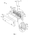
- the injection casting system 10 includes a mold unit 12 which comprises top side 14, bottom side 16, longitudinal sides 18, an inner face 22, and an outer face 24.
- the mold unit is typically stainless steel.
- a cavity 26 extends into the inner face 22.
- the cavity 26 is defined by inset bottom side 28, inset longitudinal sides 30, and an inset back face 32. As most clearly seen in Figure 3, the cavity 26 has an open face 34 and an open top side 36.
- the inset back face 32 may have aperture 38 further inset into the cavity 26.
- the cavity has a dispensing channel 40 extending from the top side 14 into the cavity 26.
- the dispensing channel 40 may parallel the longitudinal sides 30.
- the cavity 26 has a running channel 42 adjacent to the dispensing channel 40.
- the running channel 42 may parallel the bottom side 28.
- the running channel 42 may be used without a dispensing channel 40.
- a liquid dispenser 44 is provided having a reservoir 46 and a needle 48.
- the liquid dispenser 44 is positioned over the dispensing channel 40 and inserted such that the needle 48 comes in contact with the running channel 42.
- the reservoir 46 stores the encapsulation material or epoxy 54 and the dispensing needle 48 provides a throughway for dispensing the epoxy 54 in a controlled manner to the running channel 42.
- a plate 50 is provided for securing to the inner face 22 of the mold unit 12 over the open face 34 of the cavity 26.
- the plate 50 is typically stainless steel.
- the substrate material 52 Positioned intermediate the mold unit 12 and the plate 50 is the substrate material 52. As shown in Figure 1, the substrate material 52 is a printed circuit board. The substrate material may be other devices.
- each cavity 26 may have an arrangement of repeating apertures.
- each cavity 26 consists of many potential devices.
- the apertures may be arranged in a longitudinal series, a lateral series, or a combination longitudinal and lateral series.
- each cavity 26 is designed to maximize the number of parts while minimizing defects from warpage.
- defects from warpage are especially troublesome because clear molding epoxy typically has an expansion coefficient of around 60 x 10 -6 /°C. This warpage is minimized by pressing the PCB firmly between the plate 50 and mold unit 12.
- the seal may also be assisted by tenting material (not shown) a kind of dry film solder mask on PCB substrate to create a better seal.
- the tenting material is typically around 0.002 inches thick.
- the method of using the injection casting system begins with the liquid dispenser 44 in alignment with the dispensing channel 40.
- a thin mold release agent is applied uniformly across the mold surface and specifically upon the cavity 26 and aperture 38 areas.
- the PCB 52 and plate 50 are then aligned and placed upon the mold unit 12. Once the mold unit 12, PCB 52, and plate 50 are aligned, they may be placed together securely by screws, a press vice, or other system.
- the molds are preheated depending on the viscosity of the encapsulation material or epoxy 54. However, preheating the mold unit 12 may not be necessary if the viscosity of the encapsulation material 54 is thin enough to flow readily into the cavity 26.
- the dispensing needle 48 is inserted into the dispensing channel 40.
- the dispensing needle 48 is typically positioned at the bottom of the dispensing channel 40 so that it contacts the running channel 42.
- the epoxy 54 is then distributed from the reservoir 46 through the needle 48 to begin filling the running channel 42 and the cavity 26. As epoxy 54 fills the cavity 26 it flows upward against gravity and presses air upward from the cavity 26. The epoxy 54 is applied gradually so that few if any air bubbles and moisture are left within the cavity 26 and the apertures 38. Once the encapsulation material 54 fills the cavity it will enter into an overflow area 58. A divider 56 prevents any encapsulation material 54 from traveling into a neighboring cavity 26.
- the user may then remove excess material if present in the overflow area 58.
- the encapsulating material 54 can then be cured a short time in the mold and then removed for a longer cure.
Landscapes
- Engineering & Computer Science (AREA)
- Health & Medical Sciences (AREA)
- Manufacturing & Machinery (AREA)
- Ophthalmology & Optometry (AREA)
- Mechanical Engineering (AREA)
- Encapsulation Of And Coatings For Semiconductor Or Solid State Devices (AREA)
- Moulds For Moulding Plastics Or The Like (AREA)
- Casting Or Compression Moulding Of Plastics Or The Like (AREA)
- Injection Moulding Of Plastics Or The Like (AREA)
Applications Claiming Priority (2)
| Application Number | Priority Date | Filing Date | Title |
|---|---|---|---|
| US10/831,002 US7153462B2 (en) | 2004-04-23 | 2004-04-23 | Injection casting system for encapsulating semiconductor devices and method of use |
| US831002 | 2004-04-23 |
Publications (2)
| Publication Number | Publication Date |
|---|---|
| EP1589569A2 true EP1589569A2 (de) | 2005-10-26 |
| EP1589569A3 EP1589569A3 (de) | 2007-01-17 |
Family
ID=34940504
Family Applications (1)
| Application Number | Title | Priority Date | Filing Date |
|---|---|---|---|
| EP05251038A Withdrawn EP1589569A3 (de) | 2004-04-23 | 2005-02-23 | Druckgiessmaschine zum Einkapseln von Halbleiterelementen und Anwendungsmethode |
Country Status (5)
| Country | Link |
|---|---|
| US (1) | US7153462B2 (de) |
| EP (1) | EP1589569A3 (de) |
| JP (1) | JP4185501B2 (de) |
| KR (1) | KR100677007B1 (de) |
| TW (1) | TWI264804B (de) |
Cited By (3)
| Publication number | Priority date | Publication date | Assignee | Title |
|---|---|---|---|---|
| DE102008026841A1 (de) | 2008-02-22 | 2009-08-27 | Osram Opto Semiconductors Gmbh | Optoelektronisches Bauteil |
| DE102008035255A1 (de) | 2008-07-29 | 2010-03-11 | Osram Opto Semiconductors Gmbh | Optoelektronisches Halbleiterbauelement |
| DE102008064956B3 (de) | 2008-07-29 | 2023-08-24 | OSRAM Opto Semiconductors Gesellschaft mit beschränkter Haftung | Optoelektronisches halbleiterbauelement und verfahren zur herstellung eines optoelektronischen halbleiterbauelements |
Families Citing this family (4)
| Publication number | Priority date | Publication date | Assignee | Title |
|---|---|---|---|---|
| US7833456B2 (en) * | 2007-02-23 | 2010-11-16 | Micron Technology, Inc. | Systems and methods for compressing an encapsulant adjacent a semiconductor workpiece |
| TW201136077A (en) * | 2010-04-01 | 2011-10-16 | Hon Hai Prec Ind Co Ltd | Device and method for manufacturing optical couple connetor |
| JP2012164769A (ja) * | 2011-02-04 | 2012-08-30 | Murata Mfg Co Ltd | 高周波モジュールの製造方法 |
| DE102012008639A1 (de) * | 2012-05-02 | 2013-11-07 | Heraeus Noblelight Gmbh | Verfahren zur Herstellung eines optischen Moduls mit einer Silikonoptik |
Family Cites Families (17)
| Publication number | Priority date | Publication date | Assignee | Title |
|---|---|---|---|---|
| US4268942A (en) * | 1979-09-04 | 1981-05-26 | Western Electric Company, Inc. | Method and apparatus for manufacturing boxed encapsulated capacitors |
| US4374080A (en) * | 1981-01-13 | 1983-02-15 | Indy Electronics, Inc. | Method and apparatus for encapsulation casting |
| US4560138A (en) * | 1983-11-25 | 1985-12-24 | Depuglia Gaston D | Encapsulation mold |
| JPS62162337A (ja) * | 1986-01-10 | 1987-07-18 | Sharp Corp | Bステ−ジ状樹脂による電子装置の外装方法 |
| US5407505A (en) * | 1990-11-14 | 1995-04-18 | Alliedsignal Inc. | Method of encapsulating temperature sensitive devices in wax-like material having a high coefficient of fusion |
| US5663106A (en) * | 1994-05-19 | 1997-09-02 | Tessera, Inc. | Method of encapsulating die and chip carrier |
| US5665653A (en) * | 1995-03-29 | 1997-09-09 | Unifet, Incorporated | Method for encapsulating an electrochemical sensor |
| US5766987A (en) * | 1995-09-22 | 1998-06-16 | Tessera, Inc. | Microelectronic encapsulation methods and equipment |
| US5855924A (en) * | 1995-12-27 | 1999-01-05 | Siemens Microelectronics, Inc. | Closed-mold for LED alphanumeric displays |
| US5817545A (en) * | 1996-01-24 | 1998-10-06 | Cornell Research Foundation, Inc. | Pressurized underfill encapsulation of integrated circuits |
| US5998242A (en) * | 1997-10-27 | 1999-12-07 | Lsi Logic Corporation | Vacuum assisted underfill process and apparatus for semiconductor package fabrication |
| US6329224B1 (en) * | 1998-04-28 | 2001-12-11 | Tessera, Inc. | Encapsulation of microelectronic assemblies |
| US6508970B2 (en) | 1999-07-15 | 2003-01-21 | Infineon Technologies North America Corp. | Liquid transfer molding system for encapsulating semiconductor integrated circuits |
| JP3956335B2 (ja) * | 2000-03-06 | 2007-08-08 | シャープ株式会社 | 樹脂注型用金型を用いた半導体装置の製造方法 |
| US6342670B1 (en) * | 2000-09-19 | 2002-01-29 | Lite-On Electronics, Inc. | Photoelectric module device |
| CA2350747C (en) * | 2001-06-15 | 2005-08-16 | Ibm Canada Limited-Ibm Canada Limitee | Improved transfer molding of integrated circuit packages |
| KR20030001039A (ko) * | 2001-06-28 | 2003-01-06 | 동부전자 주식회사 | 반도체 캡슐화 구조 |
-
2004
- 2004-04-23 US US10/831,002 patent/US7153462B2/en not_active Expired - Fee Related
-
2005
- 2005-02-22 TW TW094105219A patent/TWI264804B/zh not_active IP Right Cessation
- 2005-02-23 EP EP05251038A patent/EP1589569A3/de not_active Withdrawn
- 2005-03-17 JP JP2005077701A patent/JP4185501B2/ja not_active Expired - Fee Related
- 2005-04-22 KR KR1020050033700A patent/KR100677007B1/ko not_active Expired - Fee Related
Cited By (8)
| Publication number | Priority date | Publication date | Assignee | Title |
|---|---|---|---|---|
| DE102008026841A1 (de) | 2008-02-22 | 2009-08-27 | Osram Opto Semiconductors Gmbh | Optoelektronisches Bauteil |
| DE102008035255A1 (de) | 2008-07-29 | 2010-03-11 | Osram Opto Semiconductors Gmbh | Optoelektronisches Halbleiterbauelement |
| US9099622B2 (en) | 2008-07-29 | 2015-08-04 | Osram Opto Semiconductors Gmbh | Optoelectronic semiconductor component |
| CN105977367A (zh) * | 2008-07-29 | 2016-09-28 | 欧司朗光电半导体有限公司 | 光电子半导体器件及其制造方法 |
| US9831394B2 (en) | 2008-07-29 | 2017-11-28 | Osram Opto Semiconductors Gmbh | Optoelectronic semiconductor component |
| US10580941B2 (en) | 2008-07-29 | 2020-03-03 | Osram Oled Gmbh | Optoelectronic semiconductor component |
| DE102008035255B4 (de) | 2008-07-29 | 2021-10-07 | OSRAM Opto Semiconductors Gesellschaft mit beschränkter Haftung | Optoelektronisches Halbleiterbauelement und Verfahren zur Herstellung eines optoelektronischen Halbleiterbauelements |
| DE102008064956B3 (de) | 2008-07-29 | 2023-08-24 | OSRAM Opto Semiconductors Gesellschaft mit beschränkter Haftung | Optoelektronisches halbleiterbauelement und verfahren zur herstellung eines optoelektronischen halbleiterbauelements |
Also Published As
| Publication number | Publication date |
|---|---|
| JP2005306018A (ja) | 2005-11-04 |
| US20050238747A1 (en) | 2005-10-27 |
| TW200536066A (en) | 2005-11-01 |
| US7153462B2 (en) | 2006-12-26 |
| JP4185501B2 (ja) | 2008-11-26 |
| EP1589569A3 (de) | 2007-01-17 |
| KR20060047440A (ko) | 2006-05-18 |
| TWI264804B (en) | 2006-10-21 |
| KR100677007B1 (ko) | 2007-02-01 |
Similar Documents
| Publication | Publication Date | Title |
|---|---|---|
| KR102157944B1 (ko) | 수지 밀봉 방법 | |
| CN106426710B (zh) | 树脂成型装置及树脂成型方法以及成型模 | |
| CN101807534B (zh) | 光学器件模塑系统 | |
| JP6560498B2 (ja) | 樹脂封止方法及び樹脂成形品の製造方法 | |
| TWI688056B (zh) | 樹脂成型裝置及樹脂成型品的製造方法 | |
| KR102684590B1 (ko) | 수지 성형품의 제조 방법, 성형 다이 및 수지 성형 장치 | |
| US6478562B1 (en) | Resin molding machine | |
| CN112840441B (zh) | 搬运装置、树脂成形装置、搬运方法及树脂成形品的制造方法 | |
| WO2016103823A1 (ja) | 樹脂成形装置及び樹脂成形方法 | |
| CN105228805A (zh) | 树脂模制装置和树脂模制方法 | |
| JP2002043345A (ja) | 半導体装置の製造方法及び樹脂封止装置 | |
| US7153462B2 (en) | Injection casting system for encapsulating semiconductor devices and method of use | |
| TW201923991A (zh) | 樹脂成型裝置及樹脂成型品的製造方法 | |
| WO2020217703A1 (ja) | 樹脂成形装置及び樹脂成形品の製造方法 | |
| JP5953601B2 (ja) | 樹脂モールド装置及び樹脂モールド方法 | |
| TW202019657A (zh) | 成型模、樹脂成型裝置、樹脂成型品的製造方法 | |
| CN108858949B (zh) | 树脂成形用成形模具及其调整方法、树脂成形装置、以及树脂成形品制造方法 | |
| WO2016125571A1 (ja) | 樹脂成形金型、樹脂成形方法、および成形品の製造方法 | |
| JP2017193078A (ja) | 樹脂モールド装置及び樹脂モールド方法 | |
| WO2012128444A1 (ko) | 봉지재 성형 방법 | |
| CN100536100C (zh) | 电子元件的树脂密封成形装置 | |
| JP6397808B2 (ja) | 樹脂成形金型および樹脂成形方法 | |
| KR20260025296A (ko) | 수지 성형 시스템 및 수지 성형품의 제조 방법 | |
| JP6901604B2 (ja) | 樹脂モールド装置及び樹脂モールド方法 | |
| KR20190075797A (ko) | 수지 성형 장치 및 수지 성형품의 제조 방법 |
Legal Events
| Date | Code | Title | Description |
|---|---|---|---|
| PUAI | Public reference made under article 153(3) epc to a published international application that has entered the european phase |
Free format text: ORIGINAL CODE: 0009012 |
|
| AK | Designated contracting states |
Kind code of ref document: A2 Designated state(s): AT BE BG CH CY CZ DE DK EE ES FI FR GB GR HU IE IS IT LI LT LU MC NL PL PT RO SE SI SK TR |
|
| AX | Request for extension of the european patent |
Extension state: AL BA HR LV MK YU |
|
| PUAL | Search report despatched |
Free format text: ORIGINAL CODE: 0009013 |
|
| AK | Designated contracting states |
Kind code of ref document: A3 Designated state(s): AT BE BG CH CY CZ DE DK EE ES FI FR GB GR HU IE IS IT LI LT LU MC NL PL PT RO SE SI SK TR |
|
| AX | Request for extension of the european patent |
Extension state: AL BA HR LV MK YU |
|
| 17P | Request for examination filed |
Effective date: 20070717 |
|
| AKX | Designation fees paid |
Designated state(s): DE FR GB IT |
|
| 17Q | First examination report despatched |
Effective date: 20071113 |
|
| STAA | Information on the status of an ep patent application or granted ep patent |
Free format text: STATUS: THE APPLICATION IS DEEMED TO BE WITHDRAWN |
|
| 18D | Application deemed to be withdrawn |
Effective date: 20080326 |