EP1591191A1 - Fügeverfahren mittels eines Au-Sn-Hartlötmaterials, dessen Dicke u.a. abhängig von dem Sn-Gehalt ist - Google Patents
Fügeverfahren mittels eines Au-Sn-Hartlötmaterials, dessen Dicke u.a. abhängig von dem Sn-Gehalt ist Download PDFInfo
- Publication number
- EP1591191A1 EP1591191A1 EP05002819A EP05002819A EP1591191A1 EP 1591191 A1 EP1591191 A1 EP 1591191A1 EP 05002819 A EP05002819 A EP 05002819A EP 05002819 A EP05002819 A EP 05002819A EP 1591191 A1 EP1591191 A1 EP 1591191A1
- Authority
- EP
- European Patent Office
- Prior art keywords
- thickness
- brazing material
- joining
- composition
- content
- Prior art date
- Legal status (The legal status is an assumption and is not a legal conclusion. Google has not performed a legal analysis and makes no representation as to the accuracy of the status listed.)
- Granted
Links
Images





Classifications
-
- B—PERFORMING OPERATIONS; TRANSPORTING
- B23—MACHINE TOOLS; METAL-WORKING NOT OTHERWISE PROVIDED FOR
- B23K—SOLDERING OR UNSOLDERING; WELDING; CLADDING OR PLATING BY SOLDERING OR WELDING; CUTTING BY APPLYING HEAT LOCALLY, e.g. FLAME CUTTING; WORKING BY LASER BEAM
- B23K35/00—Rods, electrodes, materials, or media, for use in soldering, welding, or cutting
- B23K35/22—Rods, electrodes, materials, or media, for use in soldering, welding, or cutting characterised by the composition or nature of the material
- B23K35/24—Selection of soldering or welding materials proper
- B23K35/30—Selection of soldering or welding materials proper with the principal constituent melting at less than 1550°C
- B23K35/3013—Au as the principal constituent
-
- B—PERFORMING OPERATIONS; TRANSPORTING
- B23—MACHINE TOOLS; METAL-WORKING NOT OTHERWISE PROVIDED FOR
- B23K—SOLDERING OR UNSOLDERING; WELDING; CLADDING OR PLATING BY SOLDERING OR WELDING; CUTTING BY APPLYING HEAT LOCALLY, e.g. FLAME CUTTING; WORKING BY LASER BEAM
- B23K35/00—Rods, electrodes, materials, or media, for use in soldering, welding, or cutting
- B23K35/001—Interlayers, transition pieces for metallurgical bonding of workpieces
- B23K35/004—Interlayers, transition pieces for metallurgical bonding of workpieces at least one of the workpieces being of a metal of the iron group
-
- B—PERFORMING OPERATIONS; TRANSPORTING
- B23—MACHINE TOOLS; METAL-WORKING NOT OTHERWISE PROVIDED FOR
- B23K—SOLDERING OR UNSOLDERING; WELDING; CLADDING OR PLATING BY SOLDERING OR WELDING; CUTTING BY APPLYING HEAT LOCALLY, e.g. FLAME CUTTING; WORKING BY LASER BEAM
- B23K35/00—Rods, electrodes, materials, or media, for use in soldering, welding, or cutting
- B23K35/001—Interlayers, transition pieces for metallurgical bonding of workpieces
Definitions
- the present invention relates to a method of joining by use of an Au-Sn brazing material, for example, in joining a lead pin to a circuit terminal or sealing a semiconductor package.
- Au-Sn brazing materials are brazing materials in which eutectic structures of Au-Sn alloys are used, and have relatively low melting points (about 280°C).
- Au-Sn brazing materials are excellent in corrosion resistance and have the advantage that they do not contain harmful substances such as Pb unlike solders (Sn-37 wt% Pb) that have thitherto been used.
- Au-Sn brazing materials are widely used in the field of electrical and electronic equipment and have been field proven, for example, as sealing materials for the hermetic sealing of electronic part packages and joining materials for joining lead pins to circuit terminals.
- an Au-Sn alloy phase having a high Au content (hereinafter referred to as an Au rich phase) may sometimes occur partially.
- This Au rich phase which is a kind of intermetallic compound, is hard and has a higher melting point than the surrounding Au-Sn eutectic phase. Therefore, this Au rich phase does not dissolve at the melting points of brazing materials and remains as a solid phase. And because the Au rich phase is diverse in size, variations may sometimes be produced in the thickness of a joint.
- joining is often performed by plating parts to be joined with gold in order to improve wettability.
- the present applicant has so far disclosed a sealing method and a joining method that are effective in the above-described uses (Japanese Patent No. 3086086, Japanese Patent Laid-Open No. 2001-176999).
- Japanese Patent No. 3086086, Japanese Patent Laid-Open No. 2001-176999 compared to Au-Sn brazing materials of Au-20 wt% Sn that have hitherto been used, there are used brazing materials having a composition slightly displaced from a eutectic point, in which the gold content is lowered and the Sn content is raised to 20.5 through 21.5%.
- a joint formed by these methods has a complete eutectic structure or a eutectic structure containing a small amount of Sn rich phase.
- an Sn rich phase has a low melting point, exerts a small effect and suppresses the coarsening of a structure by suppressing the occurrence of an Au rich phase. Therefore, by causing a joint having such a structure like an Sn rich phase to be formed, it becomes possible to perform joining in a stable manner.
- the methods disclosed by the present applicant can efficiently form good joints although the methods are simple ones that involve slightly changing the composition of a brazing material to be used.
- the composition of a brazing material to be used.
- an Au rich phase occurs and satisfactory joints may not be formed.
- the fraction defective itself on that occasion is not high, from the standpoint of ensuring product yield and effective utilization of resources, it is desirable to cause the fraction defective to approach zero as far as possible if this is possible.
- the present invention has been made against the above-described background and has as its object the provision of a joining method using an Au-Sn brazing material that completely suppresses the occurrence of an Au rich phase and can form a homogeneous joint with higher probability.
- the present inventor investigated the reason why joining defects occur with a brazing material in which the Sn content is slightly higher than that of an eutectic composition, and drew the following two conclusions.
- the first conclusion is that a composition (Au-20 wt% Sn) that has hitherto been regarded as a eutectic composition does not show a complete eutectic structure free from an Au rich phase and that a composition a little displaced from this shows a true eutectic structure.
- This view was obtained from the results of repeated demonstration tests by the present inventor, which will be described later, and Au-Sn alloys show a complete eutectic structure at 20.65 wt% regardless of the cooling rate and the size of cast alloys.
- the composition of the joint is such that the gold content becomes higher than the brazing material composition before the joining and the amount of the change in this gold content varies depending on the thickness of the gold plating. That is, the amount of diffused gold increases in proportion to the thickness of the gold plating and the gold content of the joint exceeds an intended gold content, causing a gold rich phase to occur readily. In other words, it might be thought that the reason why joint defects may sometimes occur in conventional methods is that the thickness of the gold plating during joining is too large.
- the invention provides a method of joining members to be joined by use of an Au-Sn brazing material, in which joining is performed by adjusting the composition and thickness of the Au-Sn brazing material so that the Sn content of a joint after joining is from 20.65 to 23.5 wt%.
- the reason why the composition of the joint is kept in this range is that the true eutectic point of this alloy system is 20.65 wt% Sn, as is apparent from the results of the investigations by the present inventor.
- the specified upper limit of the Sn content is 23.5 wt%. This is because if the Sn content exceeds 23.5 wt%, the liquidus line temperature of a brazing material becomes a high temperature of not less than 320°C, causing joining defects.
- the composition of the brazing material is kept in the above-described range when joining is performed without the plating of the members to be joined with gold.
- the present inventor examined the relationship between plating thickness and brazing material thickness for each composition of the brazing material to be used in a case where the members to be joined are plated with gold, and studied the conditions under which the composition of a joint after joining falls in the above-described range.
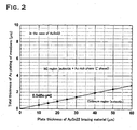
- brazing materials to be used have an Sn content of 21 wt% to 23 wt%, it is preferable to adjust the thickness of the gold plating in the ranges that satisfy the following equations.
- the relationship between the thickness of the brazing material and the thickness of the thickness of the gold plating in this case is as shown in FIGS. 1 to 3. At 21 wt% of Sn y ⁇ 0.0126 x At 22 wt% of Sn y ⁇ 0.0480 x At 23 wt% of Sn y ⁇ 0.0825 x (x: thickness of brazing material, y: thickness of gold plating)
- brazing materials to be used have an Sn content exceeding 24 wt%
- the reason why the definition by two numerical expressions is necessary like this is that because the Sn content becomes high in these brazing materials, an Sn rich phase occurs in a large amount even when the thickness of the gold plating is increased, thereby requiring an equation in which the effect of an Sn rich phase is considered.
- the relationship between the thickness of the brazing material and the thickness of the thickness of the gold plating in this case is as shown in FIGS. 4 and 5.
- the thickness of the gold plating differs depending on the kind of members to be joined, and it also differs according to the wettability and the like required even in the case of the same kind of members to be joined.
- gold plating In fixing lead pins or sealing semiconductor packages, gold plating of 0.05 to 3.0 ⁇ m is applied.
- the gold plating thickness ranges from small to relatively large sizes. In the invention, therefore, joining is performed in such a manner that the thickness of the gold plating on members to be joined is first determined and after that, the composition and thickness of the brazing material to be used are appropriately selected.
- the thickness of the gold plating in the invention is a total of the plating layers separately applied to both of the lead pin and the circuit substrate because joining is performed after both the lead pin and the circuit substrate are plated with gold.
- the composition of a brazing material can be adjusted by controlling the composition of a melt during melting and casting. Also, it is possible to appropriately vary the thickness of a brazing material in the manufacturing process.
- the conditions and the process may be generally conventional. That is, joining is generally performed in a temperature range of 300 to 320°C under an inert atmosphere of nitrogen or hydrogen gas or vacuum.
- joining in the joining process using an Au-Sn brazing material, joining can be completed without causing a gold rich phase to occur in a joint. As a result of this, it is possible to suppress joining defects ascribable to the nonuniformity of the thickness of the joint. According to the invention, it is possible to lower a fraction defective of about 2% in conventional methods to one tenth and hence it is possible to improve product yield and ensure manufacturing efficiency.
- the invention there are multiple factors capable of being varied, such as whether plating with gold is performed, the thickness of the gold plating, and the composition and thickness of the brazing material and, therefore, when a brazing material of precision shape is used and when the workability of a brazing material is required, it is possible to use a brazing material of low Sn content.
- a joining method of the invention in a flexible manner.
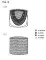
- Figure 6 (a) schematically shows a sectional structure of an ingot made obtained by casting an Au-20 wt% Sn alloy, which has hitherto been considered to have a eutectic composition.
- the composition has no uniformity and alloy layers having different structures were formed.
- a layer made of an Au-20.65 wt% Sn alloy was formed. Therefore, when an Au-20.65 wt% Sn alloy was cast, an alloy ingot having a uniform composition could be obtained as shown in FIG. 6 (b).
- Joining test Next, semiconductor packages were sealed by use of Au-Sn brazing materials having various compositions and thicknesses and the structures of joints were observed.
- the brazing materials used in this test were obtained by rolling Au-Sn alloy ingots of prescribed compositions, which are produced by the melting and casting process, to a prescribed thicknesses in sheet form and blanking the sheets into brazing materials in angular ring form.
- both the base and the cap are made of Kovar and only the cap was plated with gold before joining.
- the brazing material after working was interposed between the base and the cap plated with gold, and joining was performed by heating them to 310°C by use of a conveyor furnace.
- Table 1 shows results of an observation of the structures of joints that depend on the composition and thickness of the Au-Sn brazing materials and the thickness of the gold plating on the cap, which were examined in this embodiment.
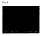
- FIGS. 7 to 9 each show a photograph of a sectional structure of a joint observed in this test, respectively, an almost complete eutectic structure (the structure indicated by ⁇ in FIG. 7 and Table 1), a structure in which an Au rich phase is mixed into a eutectic structure (the structure indicated by ⁇ in FIG. 8 and Table 1), and a structure in which an Sn rich phase is mixed into a eutectic structure (the structure indicated by ⁇ in FIG. 9 and Table 1).
- compositions etc. of the brazing materials examined in this embodiment are within the optimum ranges described in the present application and some are outside the ranges, it became apparent from the results of the examination that by ensuring brazing material thicknesses and gold plating thicknesses that fall in optimum ranges for the brazing materials of each composition, it is possible to obtain joints having a good eutectic structure in which an Au rich phase does not occur.
Landscapes
- Engineering & Computer Science (AREA)
- Mechanical Engineering (AREA)
- Electric Connection Of Electric Components To Printed Circuits (AREA)
Applications Claiming Priority (2)
| Application Number | Priority Date | Filing Date | Title |
|---|---|---|---|
| JP2004044600 | 2004-02-20 | ||
| JP2004044600 | 2004-02-20 |
Publications (2)
| Publication Number | Publication Date |
|---|---|
| EP1591191A1 true EP1591191A1 (de) | 2005-11-02 |
| EP1591191B1 EP1591191B1 (de) | 2008-04-02 |
Family
ID=34858067
Family Applications (1)
| Application Number | Title | Priority Date | Filing Date |
|---|---|---|---|
| EP05002819A Expired - Lifetime EP1591191B1 (de) | 2004-02-20 | 2005-02-10 | Fügeverfahren mittels eines Au-Sn-Hartlötmaterials, dessen Dicke u.a. abhängig von dem Sn-Gehalt ist |
Country Status (3)
| Country | Link |
|---|---|
| US (1) | US7114644B2 (de) |
| EP (1) | EP1591191B1 (de) |
| DE (1) | DE602005005733T2 (de) |
Families Citing this family (3)
| Publication number | Priority date | Publication date | Assignee | Title |
|---|---|---|---|---|
| JP4285753B2 (ja) * | 2004-06-21 | 2009-06-24 | 田中貴金属工業株式会社 | ハーメチックシールカバー及びその製造方法 |
| US8110022B2 (en) * | 2009-04-16 | 2012-02-07 | Genesis Fueltech, Inc. | Hydrogen purifier module and method for forming the same |
| JP5708692B2 (ja) | 2013-03-28 | 2015-04-30 | Tdk株式会社 | 電子デバイス用の接合構造及び電子デバイス |
Citations (4)
| Publication number | Priority date | Publication date | Assignee | Title |
|---|---|---|---|---|
| JPH06126485A (ja) * | 1992-10-19 | 1994-05-10 | Tanaka Kikinzoku Kogyo Kk | リードピン用ろう材 |
| US5794839A (en) * | 1994-08-01 | 1998-08-18 | Nippondenso Co., Ltd. | Bonding material and bonding method for electric element |
| USH1934H1 (en) * | 1992-05-01 | 2001-01-02 | Lucent Technologies, Inc. | Gold-tin solder suitable for self-aligning applications |
| US20020190106A1 (en) * | 2000-11-27 | 2002-12-19 | Shozaburo Iwai | Method for hermetic sealing of electronic parts |
Family Cites Families (6)
| Publication number | Priority date | Publication date | Assignee | Title |
|---|---|---|---|---|
| US5234153A (en) * | 1992-08-28 | 1993-08-10 | At&T Bell Laboratories | Permanent metallic bonding method |
| TWI248842B (en) * | 2000-06-12 | 2006-02-11 | Hitachi Ltd | Semiconductor device and semiconductor module |
| JP4416373B2 (ja) * | 2002-03-08 | 2010-02-17 | 株式会社日立製作所 | 電子機器 |
| US7187496B2 (en) * | 2002-03-14 | 2007-03-06 | Tdk Corporation | Manufacturing method of optical device, optical device, manufacturing method of faraday rotator, and optical communication system |
| JP2004031696A (ja) * | 2002-06-26 | 2004-01-29 | Kyocera Corp | 熱電モジュール及びその製造方法 |
| JP4014549B2 (ja) * | 2003-09-18 | 2007-11-28 | 富士電機システムズ株式会社 | ヒートシンク及びその製造方法 |
-
2005
- 2005-02-10 DE DE602005005733T patent/DE602005005733T2/de not_active Expired - Lifetime
- 2005-02-10 EP EP05002819A patent/EP1591191B1/de not_active Expired - Lifetime
- 2005-02-11 US US11/055,945 patent/US7114644B2/en not_active Expired - Lifetime
Patent Citations (4)
| Publication number | Priority date | Publication date | Assignee | Title |
|---|---|---|---|---|
| USH1934H1 (en) * | 1992-05-01 | 2001-01-02 | Lucent Technologies, Inc. | Gold-tin solder suitable for self-aligning applications |
| JPH06126485A (ja) * | 1992-10-19 | 1994-05-10 | Tanaka Kikinzoku Kogyo Kk | リードピン用ろう材 |
| US5794839A (en) * | 1994-08-01 | 1998-08-18 | Nippondenso Co., Ltd. | Bonding material and bonding method for electric element |
| US20020190106A1 (en) * | 2000-11-27 | 2002-12-19 | Shozaburo Iwai | Method for hermetic sealing of electronic parts |
Non-Patent Citations (1)
| Title |
|---|
| PATENT ABSTRACTS OF JAPAN vol. 018, no. 418 (M - 1650) 5 August 1994 (1994-08-05) * |
Also Published As
| Publication number | Publication date |
|---|---|
| US7114644B2 (en) | 2006-10-03 |
| DE602005005733T2 (de) | 2009-05-28 |
| EP1591191B1 (de) | 2008-04-02 |
| US20050184135A1 (en) | 2005-08-25 |
| DE602005005733D1 (de) | 2008-05-15 |
Similar Documents
| Publication | Publication Date | Title |
|---|---|---|
| US6179935B1 (en) | Solder alloys | |
| US6689488B2 (en) | Lead-free solder and solder joint | |
| US9409247B2 (en) | Joining method, method for producing electronic device and electronic part | |
| EP2474383B1 (de) | Bleifreie lötlegierung, verbindungselement und herstellungsverfahren dafür sowie elektronisches bauteil damit | |
| EP4105348B1 (de) | Bleifreie und antimonfreie lötlegierung, lötkugel und verwendung der lötlegierung als lötverbindung | |
| EP3381601B1 (de) | Lötlegierung, lötkugel und lötverbindung | |
| WO2021124923A1 (ja) | 銅/セラミックス接合体、及び、絶縁回路基板 | |
| EP1429884B1 (de) | Verbesserte zusammensetzungen, verfahren und vorrichtungen für ein bleifreies hochtemperaturlot | |
| EP3573100B1 (de) | Lötverbindungsverfahren und lötverbindung | |
| EP2322316A1 (de) | Au-ga-in-hartlötzusatzmetall | |
| JP2026048938A (ja) | 接合構造及び該接合構造を有する半導体装置 | |
| EP3031567A1 (de) | Bleifreie messinglegierung | |
| EP4105349B1 (de) | Bleifreie und antimonfreie lötlegierung, lötkugel und verwendung der lötlegierung als lötverbindung | |
| US20090286093A1 (en) | Lead-free solder | |
| US12521822B2 (en) | Sn solder paste comprising cu-co metal particles | |
| JP2007066995A (ja) | セラミックス配線基板、その製造方法及び半導体モジュール | |
| US8338966B2 (en) | Joint structure, joining material, and method for producing joining material containing bismuth | |
| JP4769469B2 (ja) | Au−Sn系ろう材による接合方法 | |
| US7114644B2 (en) | Joining method by Au-Sn brazing material | |
| EP0242525A1 (de) | Benetzungsverhalten von bei niedriger Temperatur schmelzenden Lötmitteln durch oberflächenaktive Zusätze | |
| EP4667148A1 (de) | Lötlegierung, lötkugel, lötpaste und lötverbindung | |
| CN1977368A (zh) | 软钎焊方法、芯片焊接用软钎料颗粒、芯片焊接软钎料颗粒的制造方法及电子零件 | |
| EP1798763B1 (de) | Halbleiteranordnung und Verfahren zur deren Montage | |
| WO2010122795A1 (ja) | 半導体装置 | |
| US20040096688A1 (en) | Lead-free joining material and joining method using the same |
Legal Events
| Date | Code | Title | Description |
|---|---|---|---|
| PUAI | Public reference made under article 153(3) epc to a published international application that has entered the european phase |
Free format text: ORIGINAL CODE: 0009012 |
|
| AK | Designated contracting states |
Kind code of ref document: A1 Designated state(s): AT BE BG CH CY CZ DE DK EE ES FI FR GB GR HU IE IS IT LI LT LU MC NL PL PT RO SE SI SK TR |
|
| AX | Request for extension of the european patent |
Extension state: AL BA HR LV MK YU |
|
| 17P | Request for examination filed |
Effective date: 20051124 |
|
| AKX | Designation fees paid |
Designated state(s): CH DE FR GB IT LI |
|
| GRAP | Despatch of communication of intention to grant a patent |
Free format text: ORIGINAL CODE: EPIDOSNIGR1 |
|
| GRAS | Grant fee paid |
Free format text: ORIGINAL CODE: EPIDOSNIGR3 |
|
| 17Q | First examination report despatched |
Effective date: 20051213 |
|
| RAP1 | Party data changed (applicant data changed or rights of an application transferred) |
Owner name: TANAKA KIKINZOKU KOGYO K.K. |
|
| GRAA | (expected) grant |
Free format text: ORIGINAL CODE: 0009210 |
|
| AK | Designated contracting states |
Kind code of ref document: B1 Designated state(s): CH DE FR GB IT LI |
|
| REG | Reference to a national code |
Ref country code: GB Ref legal event code: FG4D |
|
| REG | Reference to a national code |
Ref country code: CH Ref legal event code: EP |
|
| REF | Corresponds to: |
Ref document number: 602005005733 Country of ref document: DE Date of ref document: 20080515 Kind code of ref document: P |
|
| REG | Reference to a national code |
Ref country code: CH Ref legal event code: NV Representative=s name: BOHEST AG |
|
| ET | Fr: translation filed | ||
| PLBE | No opposition filed within time limit |
Free format text: ORIGINAL CODE: 0009261 |
|
| STAA | Information on the status of an ep patent application or granted ep patent |
Free format text: STATUS: NO OPPOSITION FILED WITHIN TIME LIMIT |
|
| 26N | No opposition filed |
Effective date: 20090106 |
|
| REG | Reference to a national code |
Ref country code: CH Ref legal event code: PCAR Free format text: NEW ADDRESS: HOLBEINSTRASSE 36-38, 4051 BASEL (CH) |
|
| REG | Reference to a national code |
Ref country code: FR Ref legal event code: PLFP Year of fee payment: 12 |
|
| REG | Reference to a national code |
Ref country code: FR Ref legal event code: PLFP Year of fee payment: 13 |
|
| REG | Reference to a national code |
Ref country code: DE Ref legal event code: R082 Ref document number: 602005005733 Country of ref document: DE Representative=s name: SCHMITT-NILSON SCHRAUD WAIBEL WOHLFROM PATENTA, DE |
|
| REG | Reference to a national code |
Ref country code: FR Ref legal event code: PLFP Year of fee payment: 14 |
|
| PGFP | Annual fee paid to national office [announced via postgrant information from national office to epo] |
Ref country code: DE Payment date: 20240219 Year of fee payment: 20 Ref country code: GB Payment date: 20240219 Year of fee payment: 20 Ref country code: CH Payment date: 20240301 Year of fee payment: 20 |
|
| PGFP | Annual fee paid to national office [announced via postgrant information from national office to epo] |
Ref country code: IT Payment date: 20240228 Year of fee payment: 20 Ref country code: FR Payment date: 20240220 Year of fee payment: 20 |
|
| REG | Reference to a national code |
Ref country code: DE Ref legal event code: R071 Ref document number: 602005005733 Country of ref document: DE |
|
| REG | Reference to a national code |
Ref country code: CH Ref legal event code: PL |
|
| REG | Reference to a national code |
Ref country code: GB Ref legal event code: PE20 Expiry date: 20250209 |
|
| PG25 | Lapsed in a contracting state [announced via postgrant information from national office to epo] |
Ref country code: GB Free format text: LAPSE BECAUSE OF EXPIRATION OF PROTECTION Effective date: 20250209 |