EP1594113A2 - Anzeigevorrichtung mit Schaltungsanordnung für Dithering - Google Patents
Anzeigevorrichtung mit Schaltungsanordnung für Dithering Download PDFInfo
- Publication number
- EP1594113A2 EP1594113A2 EP05009703A EP05009703A EP1594113A2 EP 1594113 A2 EP1594113 A2 EP 1594113A2 EP 05009703 A EP05009703 A EP 05009703A EP 05009703 A EP05009703 A EP 05009703A EP 1594113 A2 EP1594113 A2 EP 1594113A2
- Authority
- EP
- European Patent Office
- Prior art keywords
- dither
- pixel
- column
- group
- dither value
- Prior art date
- Legal status (The legal status is an assumption and is not a legal conclusion. Google has not performed a legal analysis and makes no representation as to the accuracy of the status listed.)
- Withdrawn
Links
Images








Classifications
-
- G—PHYSICS
- G09—EDUCATION; CRYPTOGRAPHY; DISPLAY; ADVERTISING; SEALS
- G09G—ARRANGEMENTS OR CIRCUITS FOR CONTROL OF INDICATING DEVICES USING STATIC MEANS TO PRESENT VARIABLE INFORMATION
- G09G3/00—Control arrangements or circuits, of interest only in connection with visual indicators other than cathode-ray tubes
- G09G3/20—Control arrangements or circuits, of interest only in connection with visual indicators other than cathode-ray tubes for presentation of an assembly of a number of characters, e.g. a page, by composing the assembly by combination of individual elements arranged in a matrix no fixed position being assigned to or needed to be assigned to the individual characters or partial characters
- G09G3/2007—Display of intermediate tones
- G09G3/2044—Display of intermediate tones using dithering
- G09G3/2051—Display of intermediate tones using dithering with use of a spatial dither pattern
-
- G—PHYSICS
- G09—EDUCATION; CRYPTOGRAPHY; DISPLAY; ADVERTISING; SEALS
- G09G—ARRANGEMENTS OR CIRCUITS FOR CONTROL OF INDICATING DEVICES USING STATIC MEANS TO PRESENT VARIABLE INFORMATION
- G09G3/00—Control arrangements or circuits, of interest only in connection with visual indicators other than cathode-ray tubes
- G09G3/20—Control arrangements or circuits, of interest only in connection with visual indicators other than cathode-ray tubes for presentation of an assembly of a number of characters, e.g. a page, by composing the assembly by combination of individual elements arranged in a matrix no fixed position being assigned to or needed to be assigned to the individual characters or partial characters
- G09G3/2007—Display of intermediate tones
- G09G3/2044—Display of intermediate tones using dithering
- G09G3/2051—Display of intermediate tones using dithering with use of a spatial dither pattern
- G09G3/2055—Display of intermediate tones using dithering with use of a spatial dither pattern the pattern being varied in time
Definitions
- the present invention relates to a dither processing circuit that improves gradation display of a display apparatus
- a plasma display panel (hereinafter referred to as a PDP) has received attention.
- the PDP is directly driven by a digital video signal, and gray scale of luminance which the PDP can represent is determined by bit number of pixel data of each pixel on the basis of the above digital video signal.
- a subfield method in which a unit frame display period, for example, one field (one frame) display period is divided into subfields of N-number, of which each emits light for only time corresponding to a weight of each bit digit of pixel data (N bits), thereby to drive the PDP.
- the field takes a video signal of interlaced type such as NTSC into consideration, and in a video signal of non-interlaced type, the field corresponds to a frame.
- one filed display period is divided into 8 subfields comprising subfields SF8, SF7, ⁇ , SF1 in order of a weight.
- Each of the subfields has an address period in which setting of a lit pixel and a unlit pixel according to pixel data is performed for each display line of the PDP, and a sustain period in which only the lit pixel is caused to emit light for only time corresponding to a weight of its subfield.
- light-emission drive control determining whether light emission is executed or not in its subfield is individually performed. Therefore, in one field, subfields in a "light emission state" and subfields in a "non-light emission state” are mixed. At this time, by total time of light emission executed in each subfield in one filed, a halftone luminance is represented.
- the gradation drive uses dither processing together, thereby to increase the gray scale visually and improve image quality.
- one halftone luminance is represented. For example, with four pixels adjacent to each other up and down and right and left forming a set, four dither values (for example, 0, 1, 2, and 3) composed of values (added value) different to each other are assigned to pixel data corresponding to each of this set of pixels, and added to each pixel data.
- four dither values for example, 0, 1, 2, and 3
- values (added value) different to each other are assigned to pixel data corresponding to each of this set of pixels, and added to each pixel data.
- an image to which the dither processing has been applied when the image is a static image, is not different from an original image because of a visual integral effect, so that the image of high quality can be seen.
- the image to which dither processing has been applied is a dynamic image, since user's eyes move with movement of the image, there is a problem that noise (pattern) peculiar to the dither processing becomes prominent readily.
- An object of the invention is to provide a dither processing circuit of a display apparatus which can perform good dither processing by which noise in a dynamic image is suppressed.
- a dither processing circuit is a dither processing circuit of a display apparatus for displaying a two-dimensional image on a display screen in accordance with a video signal indicative of pixel data for each pixel of a frame, comprising: dither value generating means for generating a dither value correspondingly to each pixel position for each pixel group in the frame; and adding means for adding the dither value to pixel data for each pixel of each pixel group to output the added result as dither processing pixel data, wherein the dither value generating means changes the dither value to be generated, in accordance with movement of an image which the video signal indicates.
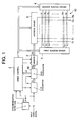
- Fig. 1 shows the general configuration of a plasma display apparatus on which a dither processing circuit according to the invention is mounted.
- the plasma display apparatus comprises a PDP 10 as a plasma display panel, and a drive part (a synchronization detecting circuit 1, a drive control circuit 2, an A/D converter 4, a data conversion circuit 30, a memory 5, an address driver 6, a first sustain driver 7, and a second sustain driver 8) which drives this plasma display panel.
- a drive part a synchronization detecting circuit 1, a drive control circuit 2, an A/D converter 4, a data conversion circuit 30, a memory 5, an address driver 6, a first sustain driver 7, and a second sustain driver 8) which drives this plasma display panel.
- the PDP 10 includes column electrodes D 1 to D m as address electrodes, and row electrodes X 1 to X n and Y 1 to Y n which are arranged orthogonal to these column electrodes.
- a pair of the row electrode X and the row electrode Y forms a row electrode corresponding to one line.
- the row electrode pair and the column electrode are coated with a dielectric layer in discharge space, and a discharge cell corresponding to a pixel is formed at the intersection of each row electrode pair with each column electrode. Namely, in the PDP 10, n ⁇ m pixels respectively corresponding to (the first row ⁇ the first column) - (the n-th row ⁇ the m-th column) are formed.
- the synchronization detecting circuit 1 when detects a vertical synchronization signal from a video signal as a unit frame data signal supplied continuously for each frame, generates a vertical synchronization signal V. Further, the synchronization detecting circuit 1, when detecting a horizontal synchronization signal from the video signal, generates a horizontal synchronization signal H. The synchronization detecting circuit 1 supplies each of these vertical synchronization signal V and horizontal synchronization signal H to the drive control circuit 2 and the data conversion circuit 30.
- the A/D converter 4 samples the video signal in accordance with a clock signal supplied from the drive control circuit 2, converts this video signal into pixel data D of each pixel, for example, 8-bit pixel data D, and supplies the pixel data to the data conversion circuit 30.
- Fig. 2 is a diagram showing the inner constitution of the data conversion circuit 30.
- the data conversion circuit 30 comprises an ABL (automatic luminance control) circuit 31, a first data conversion circuit 32, a multi gradation processing circuit 33, and a second data conversion circuit 34.
- ABL automatic luminance control
- the ABL circuit 31 adjusts a luminance level of the pixel data D of each pixel supplied sequentially from the A/D converter 4 so that the average luminance of an image displayed on a screen of the PDP 10 can be accommodated in an appropriate luminance range, and supplies a luminance adjustment pixel data D BL obtained at this time to the first data conversion circuit 32.
- Fig. 3 is a diagram showing the inner constitution of the ABL circuit 31.
- a level adjusting circuit 310 output luminance adjusted pixel data D BL obtained by adjusting the luminance level of the pixel data D in accordance with the average luminance obtained by an average luminance detecting circuit 311 described later.
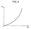
- the average luminance detecting circuit 311 firstly finds the average luminance of the inverse gamma conversion pixel data Dr.
- the average luminance detecting circuit 311 judges which of luminance modes 1-4 obtained by classifying a range of max luminance to minimum luminance into four stages the average luminance corresponds to, supplies a luminance mode signal LC representing this corresponding luminance mode to the drive control circuit 2, and supplies the above-obtained average luminance to the level adjusting circuit 310.
- the level adjusting circuit 310 supplies the pixel data D of which the luminance level has been adjusted in accordance with the average luminance, as the luminance adjusted pixel data D BL , to the data conversion circuit 312 and the first data conversion circuit 32 of the next stage.
- the first data conversion circuit 32 converts the luminance adjusted pixel data D BL , on the basis of conversion characteristic shown in Fig. 5, into first conversion pixel data D H of 9-bit of "0" to "384", and supplies this first conversion pixel data D H to the multi gradation processing circuit 33.
- the first data conversion circuit 32 data conversion is conducted according to the display gray scale in the multi gradation processing circuit 33 which will be described below and the compressed bit number by multi gradation processing.
- luminance saturation in multi gradation processing by the multi gradation processing circuit 33 and occurrence of the display characteristic at a flat portion (i.e., occurrence of gradation distortion) produced in the case that the display gradation does not exist in a bit boundary are prevented.
- the multi gradation processing circuit 33 provides the error diffusion processing and the dither processing for the 9-bit first conversion pixel data D H thereby to generate multi gradation processing pixel data D S in which the bit number is reduced to 4 bits with the present gray scale kept. These error diffusion processing and dither processing will be described later.
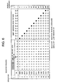
- the second data conversion circuit 34 converts the 4-bit multi gradation processing pixel data D s into display drive pixel data GD of the first to the twelfth bits in accordance with a conversion table shown in Fig. 6. Further, these first to twelfth bits respectively corresponds to subfields SF1 to SF12 described later.
- the 8-bit pixel data D capable of representing 256 gradations is converted into the 12-bit display drive pixel data GD of 13 patterns as shown in Fig. 6.
- the memory 5 writes and stores, in accordance with a writing signal supplied from the drive control circuit 2, the display drive pixel data GD sequentially.
- the memory 5 in accordance with a reading signal supplied from the drive control circuit 2, reads sequentially the display drive pixel data GD 11-nm of the same bit digit for each row, and supplies the data GD 11-nm to the address driver 6.
- the memory 5 takes the 12-bit display drive pixel data GD 11-nm of one frame as display drive pixel data DB1 11-nm to DB12 11-nm divided into 12 as follows:
- the memory 5 reads sequentially each of these DB1 11-nm , DB2 11-nm , ⁇ , and DB12 11-nm every one row in accordance with the reading signal supplied from the drive control circuit 2 to supply this to the address driver 6.
- the drive control circuit 2 generates a clock signal for the A/D converter 4 and a writing/reading signal for the memory 5 in synchronization with the horizontal synchronization signal H and the vertical synchronization signal V.
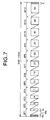
- the drive control circuit 2 supplies, in accordance with a light emission drive format shown in Fig. 7, various timing signals to drive the PDP 10 to each of the address driver 6, the first sustain driver 7 and the second sustain driver 8.
- a unit frame display period, so-called one field period is divided into 12 subfields SF1 to SF12.
- a pixel data writing step Wc in which pixel data is written into each discharge cell of the PDP 10 thereby to set "a light emission cell” and "a non-light emission cell”
- a light emission sustaining step Ic in which only the "light emission cell” is caused to emit light for only the period (by a number of times) corresponding to a weight of each subfield are executed.
- a simultaneous reset step Rc in which all the discharge cells of the PDP 10 are initialized is executed, and only in the last subfield SF12, an erasure step E is executed.
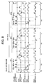
- Fig. 8 is a diagram showing application timing at which each of the address driver 6, the first sustain driver 7 and the second sustain driver 8 applies various drive pulses to the row electrode and the column electrode of the PDP.
- the first sustain driver 7 applies a reset pulse RP x of negative polarity as shown in Fig. 8 to the row electrodes X 1 to X n .
- the second sustain driver 8 applies a reset pulse RP y of positive polarity as shown in Fig. 8 to the row electrodes Y 1 to Y 2 .
- all the discharge cells in the PDP 10 are reset-discharged, and the predetermined amount of wall charges are uniformly formed in each discharge cell.
- all the discharge cells are once set "light emission cells”.
- the address driver 6 generates a pixel data pulse having a voltage corresponding to the logical level of the display drive pixel data bit DB supplied from the memory 5. At this time, the address driver 6 applies a pixel data pulse group DP composed of pixel data pulses corresponding to one line to the column electrode D 1-m .
- the address driver 6 extracts, from the display drive pixel data bit DB1 11-nm , the data corresponding to the first line, that is, DB1 11-1m , generates a pixel data pulse group DP1 1 composed of m pixel data pulses corresponding to the logical level of each of these DB1 11-1m , and applies the pixel data pulse group DP1 1 to the column electrode D 1-m .
- the address driver 6 extracts, from the display drive pixel data bit DB1 11-nm , the data corresponding to the second line, that is, DB1 21-2m , generates a pixel data pulse group DP1 2 composed of m pixel data pulses corresponding to the logical level of each of these DB1 21-2m , and applies the pixel data pulse group DP1 2 to the column electrode D 1-m .
- pixel data pulse groups DP1 3 to DP1 n are sequentially applied to the column electrode D 1-m .
- the address driver 6 in the case that the logical level of the display drive pixel data bit DB is "1", generates a pixel data pulse which is at high voltage, and in the case that the logical level of the display drive pixel data bit DB is "0", the address driver 6 generates a pixel data pulse which is at low voltage (zero volt).
- the second sustain driver 8 generates a scanning pulse SP of negative polarity as shown in Fig. 8 at the same timing as the timing at which each of the data pulse groups DP is applied, and sequentially applies this to the row electrodes Y 1 to Y n .
- a discharge selective erasure discharge
- the second sustain driver 8 generates a scanning pulse SP of negative polarity as shown in Fig. 8 at the same timing as the timing at which each of the data pulse groups DP is applied, and sequentially applies this to the row electrodes Y 1 to Y n .
- each of the first bit to the twelfth bit in the display drive pixel data GD determines whether the selective erasure discharge is caused in the pixel data writing step Wc of each of the subfields SF1 to SF12.
- the discharge cells which have been initialized to the "light emission cell” state in the simultaneous reset step Rc, proceed to an "non-light emission cell” state.
- a discharge does not occur in discharge cells formed in the "columns" to which the pixel data pulse at low voltage has been applied, and their discharge cells remain in the present state.
- the discharge cell in the "non-light emission cell” state remains in the “non-light emission cell” state
- the discharge cell in the "light emission cell” state remains in the "light emission cell” state.
- each of the first sustain driver 7 and the second sustain driver 8 applies sustain pulses IP X and IP Y of positive polarity alternately to the row electrodes X 1 to X n and Y 1 to Y n as shown in Fig. 8.
- the number of times the sustain pulse IP is applied in the light emission sustain step Ic of each subfield SF1 to SF12 is as follows: SF1: 1, SF2: 2, SF3: 4, SF4: 7, SF5: 11, SF6: 14, SF7: 20, SF8: 25, SF9: 33, SF10: 40, SF11: 48, and SF12: 50.
- the address driver 6 In the erasure step E, the address driver 6 generates an erasure pulse AP of positive polarity as shown in Fig. 8 and applies this to the column electrode D 1-m . Further, the second sustain driver 8 generates an erasure pulse EP of negative polarity as shown in Fig. 8 simultaneously with the application timing of the erasure pulse AP, and applies this erasure pulse EP to each of the row electrodes Y 1 to Y n .
- an erasure discharge is caused in all the discharge cells in the PDP 10, the wall discharges remaining in all the discharge cells are extinguished. Namely, by the erasure discharge, all the discharge cells in the PDP 10 become the "non-light emission cells".
- light emission cell setting or “non-light emission cell” setting of each discharge cell is determined by the display drive pixel data GD shown in Fig. 6. Namely, in the case that the logical level of each bit of the display drive pixel data GD is "1”, the selective erasure discharge is caused in the pixel data writing step Wc of the subfield corresponding to bit digit of its bit, and the discharge cell is set the "non-light emission cell". On the other, in the case that the logical level of its bit is "0", since the selective erasure discharge is not caused, the discharge cell remains in the present state.
- the discharge cell in the "non-light emission cell” state remains in the “non-light emission cell” state, and the discharge cell in the "light emission cell” state remains in the "light emission cell” state.
- an opportunity when the discharge cell in the "non-light emission cell” state can be caused to proceed to the "light emission cell” state is in only the reset step Rc of the first subfield SF1.
- the discharge cell, which has once proceeded to the "non-light emission cell” state in the pixel data writing step Wc of any one of the subfields SF1 to SF12 does not proceed again to the "light emission cell” state in this one field.
- each discharge cell during a period till the selective erasure discharge is caused in the subfield shown by a black dot in the figure, becomes the "light emission cell".
- the light emission sustain step Ic of each of the subfields shown by white dots existing for that period the light emission is performed by the number of times as described above.
- gradation drive capable of representing the following luminance of 13 gradations is performed. [0:1:3:7:14:25:39:59:84:117:157:205:255]
- the pixel data D obtained on the basis of the above video signal can represent halftone of 8 bits, that is, 256 stages. Therefore, the multi gradation processing is executed by the multi gradation processing circuit 33 so that the halftone display in the vicinity of 256 gradations can be realized in a pseudo manner also by the above gradation drive of 13 stages.
- Fig. 9 is a diagram showing the inner constitution of the multi gradation processing circuit 33.
- the multi gradation processing circuit 33 comprises an error diffusion processing circuit 330 and a dither processing circuit 350.
- a data separation circuit 331 in the error diffusion processing circuit 330 separates, from the 9-bit first conversion pixel data D H supplied from the first data conversion circuit 32, the upper 7-bit data as display data, and the lower 2-bit data as error data.
- An adder 332 supplies an added value obtained by adding the lower 2-bit data as the error data in the first conversion pixel data D H , delay output from a delay circuit 334, and multiplication output of a coefficient multiplier 335 to a delay circuit 336.
- the delay circuit 336 delays the added value supplied from the adder 332 by delay time D having the same time as the clock period in the pixel data A/D converter 4, and supplies this as a delay added signal AD 1 to the coefficient multiplier 335 and a delay circuit 337.
- the coefficient multiplier 335 supplies a multiplication result obtained by multiplying the delay added signal AD 1 by the predetermined coefficient K 1 (for example, "7/16") to the adder 332.
- the delay circuit 337 supplies a result obtained by further delaying the delay added signal AD 1 by time represented by (one horizontal scanning period - the delay time D x 4) to a delay circuit 338 as a delay added signal AD 2 .
- the delay circuit 338 supplies a result obtained by further delaying the delay added signal AD 2 by the delay time D to a coefficient multiplier 339 as a delay added signal AD 3 .
- the delay circuit 338 supplies a result obtained by further delaying the delay added signal AD 2 by the time represented by the delay time D x 2 to a coefficient multiplier 340 as a delay added signal AD 4 . Further, the delay circuit 338 supplies a result obtained by further delaying the delay added signal AD 2 by the time represented by the delay time D x 3 to a coefficient multiplier 341 as a delay added signal AD 5 .
- the coefficient multiplier 339 supplies a multiplication result obtained by multiplying the delay added signal AD 3 by the predetermined coefficient K 2 (for example, "3/16") to an adder 342.
- the coefficient multiplier 340 supplies a multiplication result obtained by multiplying the delay added signal AD 4 by the predetermined coefficient K 3 (for example, "5/16") to the adder 342.
- the coefficient multiplier 341 supplies a multiplication result obtained by multiplying the delay added signal AD 5 by the predetermined coefficient K 4 (for example, "1/16") to the adder 342.
- the adder 342 supplies an added signal obtained by adding the multiplication results supplied from the coefficient multipliers 339, 340 and 341 to the delay circuit 334.
- the delay circuit 334 delays the added signal by the time comprising the delay time D to supply this to the adder 332.
- the adder 332 adds the error data (lower 2-bit data in the first conversion pixel data D H ), the delay output from the delay circuit 334, and the multiplication output of the coefficient multiplier 335.
- the adder 332 In the case that there is not carry, the adder 332 generates a carry out signal C o of logical level "0" to supply its signal to an adder 333, and in the case that there is carry, the adder 332 generates a carry out signal C o of logical level "1" to supply its signal to the adder 333.
- the adder 333 outputs data obtained by adding the carry out signal C o to the above display data (upper 7-bit data in the first conversion pixel data D H ) as 7-bit error diffusion processing pixel data ED.
- the operation of the error diffusion processing circuit 330 having the constitution will be described below with reference to the operation when error diffusion processing pixel data ED corresponding to a pixel G(j, k) of the PDP 10 as shown in Fig. 10 is found.
- 7-bit error diffusion processing pixel data ED is obtained by adding a 1-bit carry out signal C o as this addition result to the upper 7-bit data in the first conversion pixel data D H , that is, the display data corresponding to the pixel G(j, k).
- the error diffusion processing circuit 330 executes the weight addition for the error data in each of the pixels G (j, k-1), G (j-1, k+1), G (j-1, k), and G (j-1, k-1) around the pixel G (j, k), and reflects its addition result in the display data corresponding to the pixel G (j, k).
- the luminance component corresponding to the lower 2-bit data in the pixel G (j, k) is represented in a pseudo manner by the above surrounding pixels. Therefore, by the display data of the bit number than is smaller than 8 bits, that is, the display data of 7-bits, the luminance gradation equivalent to that of the 8-bit pixel data D can be represented.
- the error diffusion coefficient K 1 to K 4 to be assigned to each of the four pixels may be changed for each field (frame).
- the dither processing circuit 350 provides dither processing as described below for the error diffusion processing pixel data ED supplied from the error diffusion processing circuit 330.
- the dither processing circuit 350 generates multi gradation processing pixel data D s in which the bit number is reduced to 4-bits while the luminance gradation level equivalent to the halftone luminance represented by the 7-bit error diffusion processing pixel data ED is kept.
- one halftone luminance is represented by a plurality of pixels which are adjacent to each other.
- Fig. 11 is a diagram showing the inner constitution of the dither processing circuit 350.
- the dither processing circuit comprises a movement detecting circuit 351, a dither table memory 352, a reading circuit 353, an adder 354, and a upper bit extracting circuit 355.
- the movement detecting circuit 351 generates a movement vector signal for each pixel group in accordance with the error diffusion processing pixel data ED.
- a movement vector detecting method has been disclosed in, for example, JP-A-7-59089.
- the dither table memory 352 is a dither matrix circuit which stores 3-bit dither values capable of representing "0" to "7" for each pixel of a pixel group comprising 4 rows x 4 columns. Further, the dither table memory 352 includes a static image dither table and a dynamic image dither table which indicate dither values of sequential four frames (or four fields) of the pixel group.
- the reading circuit 353 reads a dither value from either of the static image dither table and the dynamic image dither table in accordance with the movement direction and the moving amount indicated by the movement vector signal from the movement detecting circuit 351 to supply the dither value to the adder 354. Namely, in the case that the movement amount indicated by the vector signal for each pixel group is a threshold or less, the reading circuit 353 judges its data as a static image and reads a dither value from the static image dither table. In the case that the movement amount is larger than the threshold, the reading circuit 353 judges its image as a dynamic image and reads a dither value from the dynamic image dither table. In the case of reading from the dynamic image dither table, a reading start position is shifted according the movement direction indicated by the movement vector signal, and its shift amount is determined by the movement amount.
- the adder 354 adds the dither value represented by 3 bits, which is supplied from the reading circuit 353, to the lower 3-bit data of the error diffusion processing pixel data ED.
- the adder 354 supplies this addition result as dither addition pixel data to the upper bit extracting circuit 355.
- the upper bit extracting circuit 355 extracts the upper 4-bit data from the dither addition pixel data, and outputs this extracted data as multi gradation pixel data D s .
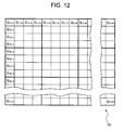
- the pixel group is basically composed of a portion of four rows ⁇ four columns in pixels G (1, 1) to G (n, m) of the PDP 10, which is surrounded by thick lines.
- a left portion of Fig. 13A shows each dither value of the first to fourth dither value groups in the static image dither table correspondingly to the pixel position.
- a left portion of Fig. 14A shows each dither value of the first to fourth dither value groups in the dynamic image dither table correspondingly to the pixel position.
- each dither table corresponds to the sequential 4 fields A to D of the video signals in time association. Further, each field and the row are judged in accordance with a vertical synchronization signal V and a horizontal synchronization signal H, and the column is judged in accordance with a clock signal.
- the reading circuit 353 judges the pixel group portion as a static image because the movement amount indicated by the movement vector signal output from the movement detecting circuit 351 is the threshold or less, the reading circuit 353 reads a dither value from the static image dither table.
- the reading circuit 353 correspondingly to the respective pixels belonging to the (4L-3)-th column, the (4L-2)-th column, the (4L-1)-th column, and the 4L-the column in the (4K)-th row of the PDP 10, reads dither values of "7", "3", "6", and "2" of the fourth row in the first dither value group in the static image dither table in that order.
- the above K is a natural number of 1 to n/4
- the above L is a natural number of 1 to m/4.
- the reading circuit 353 correspondingly to the respective pixels belonging to the (4L-3)-th column, the (4L-2)-th column, the (4L-1)-th column, and the 4L-the column in the (4K-3)-th row of the PDP 10, reads dither values of "7", "3", "6", and "2" of the first row in the second dither value group in the static image dither table in that order.
- the reading circuit 353 correspondingly to the respective pixels belonging to the (4L-3)-th column, the (4L-2)-th column, the (4L-1)-th column, and the 4L-the column in the (4K-2)-th row of the PDP 10, reads dither values of "1", "5", "0", and "4" of the second row in the second dither value group in the static image dither table in that order.
- the reading circuit 353 correspondingly to the respective pixels belonging to the (4L-3)-th column, the (4L-2)-th column, the (4L-1)-th column, and the 4L-the column in the (4K)-th row of the PDP 10, reads dither values of "6", "2", "7", and "3" of the fourth row in the second dither value group in the static image dither table in that order.
- the reading circuit 353 correspondingly to the respective pixels belonging to the (4L-3)-th column, the (4L-2)-th column, the (4L-1)-th column, and the 4L-the column in the (4K-3)-th row of the PDP 10, reads dither values of "3", "7", "2", and "6" of the first row in the third dither value group in the static image dither table in that order.
- the reading circuit 353 correspondingly to the respective pixels belonging to the (4L-3)-th column, the (4L-2)-th column, the (4L-1)-th column, and the 4L-the column in the (4K-2)-th row of the PDP 10, reads dither values of "5", "1", "4", and "0" of the second row in the third dither value group in the static image dither table in that order.
- the reading circuit 353 correspondingly to the respective pixels belonging to the (4L-3)-th column, the (4L-2)-th column, the (4L-1)-th column, and the 4L-the column in the (4K)-th row of the PDP 10, reads dither values of "4", "0", "5", and "1" of the fourth row in the third dither value group in the static image dither table in that order.
- the reading circuit 353 correspondingly to the respective pixels belonging to the (4L-3)-th column, the (4L-2)-th column, the (4L-1)-th column, and the 4L-the column in the (4K-3)-th row of the PDP 10, reads dither values of "4", "0", "5", and "1" of the first row in the fourth dither value group in the static image dither table in that order.
- the reading circuit 353 correspondingly to the respective pixels belonging to the (4L-3)-th column, the (4L-2)-th column, the (4L-1)-th column, and the 4L-the column in the (4K-2)-th row of the PDP 10, reads dither values of "2", "6", "3", and "7" of the second row in the fourth dither value group in the static image dither table in that order.
- the reading circuit 353 correspondingly to the respective pixels belonging to the (4L-3)-th column, the (4L-2)-th column, the (4L-1)-th column, and the 4L-the column in the (4K-1)-th row of the PDP 10, reads dither values of "5", "1", "4", and "0" of the third row in the fourth dither value group in the static image dither table in that order.
- the reading circuit 353 correspondingly to the respective pixels belonging to the (4L-3)-th column, the (4L-2)-th column, the (4L-1)-th column, and the 4L-the column in the (4K)-th row of the PDP 10, reads dither values of "3", "7", "2", and "6" of the fourth row in the fourth dither value group in the static image dither table in that order.
- reading circuit 353 judges its pixel group portion as a dynamic image because the movement amount indicated by the movement vector signal output from the movement detecting circuit 351 is larger than the threshold, the reading circuit 353 reads a dither value from the dynamic image dither table. Further, the reading circuit 353, correspondingly to the movement direction indicated by its movement vector signal, moves the reading start position in its direction in the four rows x the four columns in each of the first dither value group to the four dither value group. In the case that the movement direction is, for example, a right direction on the screen, reading is performed by the reading circuit 353 as follows.
- the reading circuit 353, in a first field A reads the dither values of each row in the first dither value group in the dynamic dither table in order of the first column, the second column, the third column, and the fourth column. Namely, the reading circuit 353, in the field A, correspondingly to the respective pixels belonging to the (4L-3)-th column, the (4L-2)-th column, the (4L-1)-th column, and the 4L-the column in the (4K-3)-th row of the PDP 10, reads dither values of "0", "4", "1", and "5" of the first row in the first dither value group in the dynamic image dither table in that order.
- the reading circuit 353 correspondingly to the respective pixels belonging to the (4L-3)-th column, the (4L-2)-th column, the (4L-1)-th column, and the 4L-the column in the (4K)-th row of the PDP 10, reads dither values of "7", "3", "6", and "2" of the fourth row in the first dither value group in the dynamic image dither table in that order.
- the reading circuit 353, in the next field B reads the dither values of each row in the second dither value group in the dynamic dither table in order of the second column, the third column, the fourth column, and the first column. Namely, the reading circuit 353, in the field B, correspondingly to the respective pixels belonging to the (4L-3)-th column, the (4L-2)-th column, the (4L-1)-th column, and the 4L-the column in the (4K-3)-th row of the PDP 10, reads dither values of "7", "3", "6", and "2" of the first row in the second dither value group in the dynamic image dither table in that order.
- the reading circuit 353 correspondingly to the respective pixels belonging to the (4L-3)-th column, the (4L-2)-th column, the (4L-1)-th column, and the 4L-the column in the (4K-2)-th row of the PDP 10, reads dither values of "1", "5", "0", and "4" of the second row in the second dither value group in the dynamic image dither table in that order.
- the reading circuit 353 correspondingly to the respective pixels belonging to the (4L-3)-th column, the (4L-2)-th column, the (4L-1)-th column, and the 4L-the column in the (4K)-th row of the PDP 10, reads dither values of "0", "4", "1", and "5" of the fourth row in the second dither value group in the dynamic image dither table in that order.
- the reading circuit 353, in the next field C reads the dither values of each row in the third dither value group in the dynamic dither table in order of, the third column, the fourth column, the first column, and the second column. Namely, the reading circuit 353, in the field C, correspondingly to the respective pixels belonging to the (4L-3)-th column, the (4L-2)-th column, the (4L-1)-th column, and the 4L-the column in the (4K-3)-th row of the PDP 10, reads dither values of "2", "6", "3", and "7" of the first row in the third dither value group in the dynamic image dither table in that order.
- the reading circuit 353 correspondingly to the respective pixels belonging to the (4L-3)-th column, the (4L-2)-th column, the (4L-1)-th column, and the 4L-the column in the (4K-2)-th row of the PDP 10, reads dither values of "4", "0", "5", and "1" of the second row in the third dither value group in the dynamic image dither table in that order.
- the reading circuit 353 correspondingly to the respective pixels belonging to the (4L-3)-th column, the (4L-2)-th column, the (4L-1)-th column, and the 4L-the column in the (4K)-th row of the PDP 10, reads dither values of "5", "1", "4", and "0" of the fourth row in the third dither value group in the dynamic image dither table in that order.
- the reading circuit 353, in the next field D reads the dither values of each row in the fourth dither value group in the dynamic dither table in order of the fourth column, the first column, the second column, and the third column. Namely, the reading circuit 353, in the field D, correspondingly to the respective pixels belonging to the (4L-3)-th column, the (4L-2)-th column, the (4L-1)-th column, and the 4L-the column in the (4K-3)-th row of the PDP 10, reads dither values of "4", "0", "5", and "1" of the first row in the fourth dither value group in the dynamic image dither table in that order.
- the reading circuit 353 correspondingly to the respective pixels belonging to the (4L-3)-th column, the (4L-2)-th column, the (4L-1)-th column, and the 4L-the column in the (4K-2)-th row of the PDP 10, reads dither values of "2", "6", "3", and "7" of the second row in the fourth dither value group in the dynamic image dither table in that order.
- the reading circuit 353 correspondingly to the respective pixels belonging to the (4L-3)-th column, the (4L-2)-th column, the (4L-1)-th column, and the 4L-the column in the (4K-1)-th row of the PDP 10, reads dither values of "5", "1", "4", and "0" of the third row in the fourth dither value group in the dynamic image dither table in that order.
- the reading circuit 353 correspondingly to the respective pixels belonging to the (4L-3)-th column, the (4L-2)-th column, the (4L-1)-th column, and the 4L-the column in the (4K)-th row of the PDP 10, reads dither values of "3", "7", "2", and "6" of the fourth row in the fourth dither value group in the dynamic image dither table in that order.
- the upper bit extracting circuit 355 extracts the upper 4-bit data from the pixel data of the addition result by the adder 354, its carry is reflected in the output data D s of the upper bit extracting circuit 355.
- this dither processing circuit 350 dither processing is performed with a pixel group of 4 rows x 4 columns surrounded by thick lines in Fig. 12 taken as one display unit. Namely, to the lower 3-bit data of each of the error diffusion processing pixel data ED corresponding to 16 pixels in the pixel group of 4 rows x 4 columns, the dither values of "0" to "7" represented by the 3 bits are assigned as shown in Figs. 13A and 14A, and added. When the dither values of "0" to "7” represented by the 3 bits are thus added to the lower 3-bit data of each of the error diffusion processing pixel data ED corresponding to 16 pixels, any of the following eight carry states occurs:
- the reading circuit 353 in the first field A, reads data of each row in the first dither value group in the dynamic image dither table in order of the first column, the second column, the third column, and the fourth column; in the field B, reads data of each row in the second dither value group in the dynamic image dither table in order of the fourth column, the first column, the second column, and the third column; in the field C, reads data of each row in the third dither value group in the dynamic image dither table in order of the third column, the fourth column, the first column, and the second column; and in the field D, reads data of each row in the fourth dither value group in the dynamic image dither table in order of the second column, the third column, the fourth column, and the first column.
- the reading circuit 353 in the first field A, reads the dither values of each row in the first dither value group in the dynamic image dither table in order of the first row to the fourth row and in order of the first column to the fourth column; in the field B, reads the dither values of each row in the second dither value group in the dynamic image dither table in order of the fourth row, the first row, the second row and the third row and in order of the first column to the fourth column; in the field C, reads the dither values of each row in the third dither value group in the dynamic image dither table in order of the third row, the fourth row, the first row, and the second row and in order of the first column to the fourth column; and in the field D, reads the dither values of each row in the fourth dither value group in the dynamic image dither table in order of the second row, the third row, the fourth row and the first row and in order of the first column to the fourth column;
- the reading circuit 353 in the first field A, reads the dither values of each row in the first dither value group in the dynamic image dither table in order of the first row to the fourth row and in order of the first column to the fourth column; in the field B, reads the dither values of each row in the second dither value group in the dynamic image dither table in order of the second row, the third row, the fourth row and the first row and in order of the first column to the fourth column; in the field C, reads the dither values of each row in the third dither value group in the dynamic image dither table in order of the third row, the fourth row, the first row, and the second row and in order of the first column to the fourth column; and in the field D, reads the dither values of each row in the fourth dither value group in the dynamic image dither table in order of the fourth row, the first row, and the second row and the third row and in order of the first column to the fourth column;
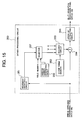
- Fig. 15 shows another constitutional example of the dither processing circuit 350.
- the dither processing circuit 350 in Fig. 15 includes a random number generating circuit 356 and a selector 357 in addition to the movement detecting circuit 351, the dither table memory 352, the reading circuit 353, the adder 354, and the upper bit extracting circuit 355 shown in Fig. 11.
- the random number generating circuit 356 outputs data indicating any of integers of 1 to 4 in a random order for each field. Namely, the output values of the random number generating circuit 356 are values in which an output order of 1 to 4 changes every four fields.
- the selector 357 judges, in accordance with the movement detecting signal from the movement detecting circuit 351, whether an image is a static image or a dynamic image and switches the field number and the output value of the random number generating circuit 356 in accordance with the judgment result to output the switched value to the reading circuit 353.
- the field number supplied to the selector 357 is data in which any integer of 1 to 4 is indicated in number order of each field and repeated every four fields.
- the selector 357 when judges an image as a static image in accordance with the movement detection signal from the movement detecting circuit 351, supplies the field number to the reading circuit 353 as it is.
- the selector 357 when judges an image as a dynamic image in accordance with the movement detection signal from the movement detecting circuit 351, supplies the output value from the random number generating circuit 356 to the reading circuit 353.
- the reading circuit 353 reads the dither value group of the number specified as the field number from the selector 357 to supply it to the adder 354.
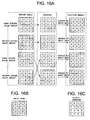
- the dither table stored in the dither table memory 352 is taken as a first dither value group to the fourth dither value group as shown in Fig. 16A.
- This table is the same as the static image dither table shown in Fig. 13A.
- the reading circuit 353 reads dither values from the first dither value group to the fourth dither value group in the dither table memory 352 in that order and supplies the dither values to the adder 354.
- the dither values are read in order of the first dither value group, the second dither value group, the fourth dither value group and the third dither value group.
- the reading circuit 353 correspondingly to the movement direction indicated by the movement vector signal, moves the reading start position in 4 rows x 4 columns in each of the first dither value group to the fourth dither value group in that direction.
- the movement direction is a right direction on the screen. Accordingly, the addition results by the adder 354 as shown in the right portion of Fig. 16A are obtained. Further, also regarding the average output of its addition result, as shown in Fig. 16C, all the pixel of 4 rows x 4 columns become "6".
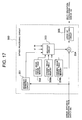
- Fig. 17 shows another constitutional example of the dither processing circuit 350.
- the dither processing circuit 350 shown in Fig. 17 includes a static image dither table memory 358 and a plurality of dynamic image dither table memories 359a, 359b, .... in addition to the movement detecting circuit 351, the reading circuit 353, the adder 354, and the upper bit extracting circuit 355 shown in Fig. 11.
- These dither table memories 358, 359a, 359b, ⁇ are memories which store 3-bit dither values which can represent "0" to "7" for each pixel of a pixel group comprising 4 rows x 4 columns.
- the dynamic image dither table memories 359a, 359b, ⁇ are provided correspondingly to difference in the movement amount of the dynamic image. Therefore, in the case of the dynamic image, the reading circuit 353 selects one dither table memory from the dynamic image dither table memories 359a, 359b, .... in accordance with the movement amount indicated by the movement detection signal from the movement detecting circuit 351, and reads the dither value from the selected dither table memory. Other operations are similar to those in the dither processing circuit shown in Fig. 11.
- Fig. 18 shows the concrete constitution of the movement detecting circuit 351 shown in Figs. 11, 15 and 17.
- the movement detecting circuit 351 includes a block average luminance level calculating part 361, a memory 362, and a comparison circuit 363.
- the block average luminance level calculating part 361 divides the frame of the video signals supplied as the error diffusion processing pixel data ED into a plurality of blocks to calculate the average luminance level of each block. Each of these blocks is a pixel group which is larger than the pixel group of the above dither matrix.
- the average luminance level of each block calculated by the block average luminance level calculating part 361 is supplied to the memory 362 and the comparison circuit 363. In the memory 362, the average luminance level of each block before the number V (horizontal scanning period).
- the comparison circuit 363 detects a level time-variation value in accordance with the present average luminance level in the same block and the average luminance level before the number V which has been stored in the memory 362, and compares the level variation value with a threshold to judge the movement.
- the invention can be applied also to another display apparatus such as a liquid crystal display apparatus.
- the dither processing circuit comprises dither value generating means which generates the dither value correspondingly to each pixel position of each pixel group on a frame, and adding means which adds the dither value to pixel data for each pixel of each pixel group to output the added result as dither processing pixel data. Since the dither value generating means changes the dither value to be generated, in accordance with the movement of the image which the video signal indicates, good dither processing by which noise in a dynamic image is suppressed can be performed.
Landscapes
- Engineering & Computer Science (AREA)
- Physics & Mathematics (AREA)
- Computer Hardware Design (AREA)
- General Physics & Mathematics (AREA)
- Theoretical Computer Science (AREA)
- Control Of Indicators Other Than Cathode Ray Tubes (AREA)
- Control Of Gas Discharge Display Tubes (AREA)
- Image Processing (AREA)
- Liquid Crystal Display Device Control (AREA)
- Transforming Electric Information Into Light Information (AREA)
Applications Claiming Priority (2)
| Application Number | Priority Date | Filing Date | Title |
|---|---|---|---|
| JP2004137275 | 2004-05-06 | ||
| JP2004137275A JP2005321442A (ja) | 2004-05-06 | 2004-05-06 | ディスプレイ装置のディザ処理回路 |
Publications (2)
| Publication Number | Publication Date |
|---|---|
| EP1594113A2 true EP1594113A2 (de) | 2005-11-09 |
| EP1594113A3 EP1594113A3 (de) | 2006-11-29 |
Family
ID=34936093
Family Applications (1)
| Application Number | Title | Priority Date | Filing Date |
|---|---|---|---|
| EP05009703A Withdrawn EP1594113A3 (de) | 2004-05-06 | 2005-05-03 | Anzeigevorrichtung mit Schaltungsanordnung für Dithering |
Country Status (3)
| Country | Link |
|---|---|
| US (1) | US20050248583A1 (de) |
| EP (1) | EP1594113A3 (de) |
| JP (1) | JP2005321442A (de) |
Cited By (1)
| Publication number | Priority date | Publication date | Assignee | Title |
|---|---|---|---|---|
| EP2113901A3 (de) * | 2008-04-29 | 2010-03-03 | Samsung Mobile Display Co., Ltd. | Flachbildschirm und Verfahren zu dessen Ansteuerung |
Families Citing this family (14)
| Publication number | Priority date | Publication date | Assignee | Title |
|---|---|---|---|---|
| KR100499102B1 (ko) * | 2003-12-15 | 2005-07-01 | 엘지전자 주식회사 | 플라즈마 디스플레이 패널의 구동장치 및 구동방법 |
| JP2006154576A (ja) * | 2004-11-30 | 2006-06-15 | Toshiba Corp | 階調補正装置および階調補正方法 |
| EP1862995A1 (de) * | 2006-05-31 | 2007-12-05 | Texas Instruments France S.A. | Verfahren und Vorrichtung mit räumlichen und zeitlichen Zittertechniken |
| TWI329853B (en) | 2006-12-28 | 2010-09-01 | Mstar Semiconductor Inc | Dithering method and related dithering module and liquid crystal display (lcd) |
| JP5176332B2 (ja) * | 2007-01-25 | 2013-04-03 | 船井電機株式会社 | 表示装置 |
| US8207931B2 (en) * | 2007-05-31 | 2012-06-26 | Hong Kong Applied Science and Technology Research Institute Company Limited | Method of displaying a low dynamic range image in a high dynamic range |
| TWI357034B (en) * | 2007-09-28 | 2012-01-21 | Mstar Semiconductor Inc | Dithering mask and method of forming the same |
| JP7007789B2 (ja) * | 2015-06-26 | 2022-01-25 | シナプティクス・ジャパン合同会社 | 表示パネルドライバ及び表示パネルの駆動方法 |
| US10839771B2 (en) * | 2016-12-22 | 2020-11-17 | Intel Corporation | Display driver |
| US10909933B2 (en) | 2016-12-22 | 2021-02-02 | Intel Corporation | Digital driver for displays |
| JP7006519B2 (ja) | 2018-06-14 | 2022-01-24 | 株式会社Jvcケンウッド | 映像信号処理装置、ディザパターン生成方法、及びディザパターン生成プログラム |
| JP7063214B2 (ja) * | 2018-09-25 | 2022-05-09 | 株式会社Jvcケンウッド | 映像信号処理装置、ディザパターン生成方法、及びディザパターン生成プログラム |
| JP7063213B2 (ja) * | 2018-09-25 | 2022-05-09 | 株式会社Jvcケンウッド | 映像信号処理装置、ディザパターン生成方法、及びディザパターン生成プログラム |
| JP7483537B2 (ja) * | 2020-07-27 | 2024-05-15 | 日本放送協会 | 画像表示装置、信号処理方法及び信号処理プログラム |
Family Cites Families (8)
| Publication number | Priority date | Publication date | Assignee | Title |
|---|---|---|---|---|
| CA2137061A1 (en) * | 1993-12-02 | 1995-06-03 | Stephen W. Marshall | Technique to increase the apparent dynamic range of a visual display |
| JPH1069251A (ja) * | 1996-08-29 | 1998-03-10 | Canon Inc | 表示装置、表示システム及び画像処理装置 |
| US6130707A (en) * | 1997-04-14 | 2000-10-10 | Philips Electronics N.A. Corp. | Video motion detector with global insensitivity |
| US6008794A (en) * | 1998-02-10 | 1999-12-28 | S3 Incorporated | Flat-panel display controller with improved dithering and frame rate control |
| JP4016493B2 (ja) * | 1998-08-05 | 2007-12-05 | 三菱電機株式会社 | ディスプレイ装置及びその多階調化回路 |
| CN1160681C (zh) * | 1999-04-12 | 2004-08-04 | 松下电器产业株式会社 | 图象显示装置 |
| JP2003015588A (ja) * | 2001-06-28 | 2003-01-17 | Pioneer Electronic Corp | ディスプレイ装置 |
| EP1387340A1 (de) * | 2002-07-30 | 2004-02-04 | Deutsche Thomson-Brandt Gmbh | Verfahren und Einrichtung zur Videodatenbearbeitung für eine Anzeigevorrichtung |
-
2004
- 2004-05-06 JP JP2004137275A patent/JP2005321442A/ja active Pending
-
2005
- 2005-05-03 EP EP05009703A patent/EP1594113A3/de not_active Withdrawn
- 2005-05-05 US US11/121,924 patent/US20050248583A1/en not_active Abandoned
Cited By (2)
| Publication number | Priority date | Publication date | Assignee | Title |
|---|---|---|---|---|
| EP2113901A3 (de) * | 2008-04-29 | 2010-03-03 | Samsung Mobile Display Co., Ltd. | Flachbildschirm und Verfahren zu dessen Ansteuerung |
| US8754903B2 (en) | 2008-04-29 | 2014-06-17 | Samsung Display Co., Ltd. | Flat panel display and method of driving the same |
Also Published As
| Publication number | Publication date |
|---|---|
| JP2005321442A (ja) | 2005-11-17 |
| EP1594113A3 (de) | 2006-11-29 |
| US20050248583A1 (en) | 2005-11-10 |
Similar Documents
| Publication | Publication Date | Title |
|---|---|---|
| JP2003015588A (ja) | ディスプレイ装置 | |
| EP1594113A2 (de) | Anzeigevorrichtung mit Schaltungsanordnung für Dithering | |
| JP3961171B2 (ja) | ディスプレイ装置の多階調処理回路 | |
| US6483248B2 (en) | Display device | |
| KR100934952B1 (ko) | 그레이 스케일 충실도 묘사를 개선하기 위한 비디오 화상처리 방법 및 장치 | |
| JP3738890B2 (ja) | プラズマディスプレイパネルの駆動方法 | |
| JP2002023693A (ja) | プラズマディスプレイパネルの駆動方法 | |
| JP3761132B2 (ja) | ディスプレイパネルの駆動方法 | |
| JP2000231362A (ja) | プラズマディスプレイパネルの駆動方法 | |
| JP3630584B2 (ja) | ディスプレイパネルの駆動方法 | |
| JP2002351381A (ja) | ディスプレイ装置及びディスプレイパネルの駆動方法 | |
| JP4071382B2 (ja) | プラズマディスプレイパネルの駆動方法 | |
| JP3734244B2 (ja) | ディスプレイパネルの駆動方法 | |
| KR100674661B1 (ko) | 표시 패널의 구동 방법 | |
| JP4731841B2 (ja) | 表示パネルの駆動装置及び駆動方法 | |
| US7109950B2 (en) | Display apparatus | |
| JP2003302929A (ja) | プラズマディスプレイ装置 | |
| KR100578917B1 (ko) | 플라즈마 디스플레이 패널의 구동 장치, 플라즈마디스플레이 패널의 화상 처리 방법 및 플라즈마디스플레이 패널 | |
| KR100850616B1 (ko) | 영상 신호 처리 장치 및 영상 신호 처리 방법 | |
| EP1732055B1 (de) | Anzeigevorrichtung | |
| JP3990612B2 (ja) | 画像評価装置 | |
| KR20070101823A (ko) | 플라즈마 디스플레이 패널의 구동 방법 | |
| JP5011636B2 (ja) | 画像表示方法 | |
| JP3727619B2 (ja) | 画像表示装置 | |
| JP2006011468A (ja) | プラズマディスプレイパネルの駆動方法 |
Legal Events
| Date | Code | Title | Description |
|---|---|---|---|
| PUAI | Public reference made under article 153(3) epc to a published international application that has entered the european phase |
Free format text: ORIGINAL CODE: 0009012 |
|
| AK | Designated contracting states |
Kind code of ref document: A2 Designated state(s): AT BE BG CH CY CZ DE DK EE ES FI FR GB GR HU IE IS IT LI LT LU MC NL PL PT RO SE SI SK TR |
|
| AX | Request for extension of the european patent |
Extension state: AL BA HR LV MK YU |
|
| PUAL | Search report despatched |
Free format text: ORIGINAL CODE: 0009013 |
|
| AK | Designated contracting states |
Kind code of ref document: A3 Designated state(s): AT BE BG CH CY CZ DE DK EE ES FI FR GB GR HU IE IS IT LI LT LU MC NL PL PT RO SE SI SK TR |
|
| AX | Request for extension of the european patent |
Extension state: AL BA HR LV MK YU |
|
| AKX | Designation fees paid | ||
| STAA | Information on the status of an ep patent application or granted ep patent |
Free format text: STATUS: THE APPLICATION IS DEEMED TO BE WITHDRAWN |
|
| 18D | Application deemed to be withdrawn |
Effective date: 20070530 |
|
| REG | Reference to a national code |
Ref country code: DE Ref legal event code: 8566 |