EP1596433A1 - Verfahren zur Erstellung einer Halbleiterscheibe aus integrierten Schaltungschips sowie nach diesem Verfahren hergestellte Vorrichtung - Google Patents
Verfahren zur Erstellung einer Halbleiterscheibe aus integrierten Schaltungschips sowie nach diesem Verfahren hergestellte Vorrichtung Download PDFInfo
- Publication number
- EP1596433A1 EP1596433A1 EP04394026A EP04394026A EP1596433A1 EP 1596433 A1 EP1596433 A1 EP 1596433A1 EP 04394026 A EP04394026 A EP 04394026A EP 04394026 A EP04394026 A EP 04394026A EP 1596433 A1 EP1596433 A1 EP 1596433A1
- Authority
- EP
- European Patent Office
- Prior art keywords
- layer
- wafer
- die
- integrated circuit
- neo
- Prior art date
- Legal status (The legal status is an assumption and is not a legal conclusion. Google has not performed a legal analysis and makes no representation as to the accuracy of the status listed.)
- Granted
Links
Images


Classifications
-
- H—ELECTRICITY
- H10—SEMICONDUCTOR DEVICES; ELECTRIC SOLID-STATE DEVICES NOT OTHERWISE PROVIDED FOR
- H10P—GENERIC PROCESSES OR APPARATUS FOR THE MANUFACTURE OR TREATMENT OF DEVICES COVERED BY CLASS H10
- H10P72/00—Handling or holding of wafers, substrates or devices during manufacture or treatment thereof
- H10P72/70—Handling or holding of wafers, substrates or devices during manufacture or treatment thereof for supporting or gripping
- H10P72/74—Handling or holding of wafers, substrates or devices during manufacture or treatment thereof for supporting or gripping using temporarily an auxiliary support
-
- H—ELECTRICITY
- H10—SEMICONDUCTOR DEVICES; ELECTRIC SOLID-STATE DEVICES NOT OTHERWISE PROVIDED FOR
- H10P—GENERIC PROCESSES OR APPARATUS FOR THE MANUFACTURE OR TREATMENT OF DEVICES COVERED BY CLASS H10
- H10P72/00—Handling or holding of wafers, substrates or devices during manufacture or treatment thereof
- H10P72/70—Handling or holding of wafers, substrates or devices during manufacture or treatment thereof for supporting or gripping
- H10P72/74—Handling or holding of wafers, substrates or devices during manufacture or treatment thereof for supporting or gripping using temporarily an auxiliary support
- H10P72/7402—Wafer tapes, e.g. grinding or dicing support tapes
-
- H—ELECTRICITY
- H10—SEMICONDUCTOR DEVICES; ELECTRIC SOLID-STATE DEVICES NOT OTHERWISE PROVIDED FOR
- H10W—GENERIC PACKAGES, INTERCONNECTIONS, CONNECTORS OR OTHER CONSTRUCTIONAL DETAILS OF DEVICES COVERED BY CLASS H10
- H10W72/00—Interconnections or connectors in packages
- H10W72/01—Manufacture or treatment
- H10W72/0198—Manufacture or treatment batch processes
-
- H—ELECTRICITY
- H10—SEMICONDUCTOR DEVICES; ELECTRIC SOLID-STATE DEVICES NOT OTHERWISE PROVIDED FOR
- H10P—GENERIC PROCESSES OR APPARATUS FOR THE MANUFACTURE OR TREATMENT OF DEVICES COVERED BY CLASS H10
- H10P72/00—Handling or holding of wafers, substrates or devices during manufacture or treatment thereof
- H10P72/70—Handling or holding of wafers, substrates or devices during manufacture or treatment thereof for supporting or gripping
- H10P72/74—Handling or holding of wafers, substrates or devices during manufacture or treatment thereof for supporting or gripping using temporarily an auxiliary support
- H10P72/7416—Handling or holding of wafers, substrates or devices during manufacture or treatment thereof for supporting or gripping using temporarily an auxiliary support used during dicing or grinding
-
- H—ELECTRICITY
- H10—SEMICONDUCTOR DEVICES; ELECTRIC SOLID-STATE DEVICES NOT OTHERWISE PROVIDED FOR
- H10P—GENERIC PROCESSES OR APPARATUS FOR THE MANUFACTURE OR TREATMENT OF DEVICES COVERED BY CLASS H10
- H10P72/00—Handling or holding of wafers, substrates or devices during manufacture or treatment thereof
- H10P72/70—Handling or holding of wafers, substrates or devices during manufacture or treatment thereof for supporting or gripping
- H10P72/74—Handling or holding of wafers, substrates or devices during manufacture or treatment thereof for supporting or gripping using temporarily an auxiliary support
- H10P72/7438—Handling or holding of wafers, substrates or devices during manufacture or treatment thereof for supporting or gripping using temporarily an auxiliary support with parts of the auxiliary support remaining in the finished device
-
- H—ELECTRICITY
- H10—SEMICONDUCTOR DEVICES; ELECTRIC SOLID-STATE DEVICES NOT OTHERWISE PROVIDED FOR
- H10W—GENERIC PACKAGES, INTERCONNECTIONS, CONNECTORS OR OTHER CONSTRUCTIONAL DETAILS OF DEVICES COVERED BY CLASS H10
- H10W72/00—Interconnections or connectors in packages
- H10W72/071—Connecting or disconnecting
- H10W72/072—Connecting or disconnecting of bump connectors
-
- H—ELECTRICITY
- H10—SEMICONDUCTOR DEVICES; ELECTRIC SOLID-STATE DEVICES NOT OTHERWISE PROVIDED FOR
- H10W—GENERIC PACKAGES, INTERCONNECTIONS, CONNECTORS OR OTHER CONSTRUCTIONAL DETAILS OF DEVICES COVERED BY CLASS H10
- H10W72/00—Interconnections or connectors in packages
- H10W72/071—Connecting or disconnecting
- H10W72/072—Connecting or disconnecting of bump connectors
- H10W72/07231—Techniques
- H10W72/07234—Using a reflow oven
-
- H—ELECTRICITY
- H10—SEMICONDUCTOR DEVICES; ELECTRIC SOLID-STATE DEVICES NOT OTHERWISE PROVIDED FOR
- H10W—GENERIC PACKAGES, INTERCONNECTIONS, CONNECTORS OR OTHER CONSTRUCTIONAL DETAILS OF DEVICES COVERED BY CLASS H10
- H10W72/00—Interconnections or connectors in packages
- H10W72/071—Connecting or disconnecting
- H10W72/072—Connecting or disconnecting of bump connectors
- H10W72/07231—Techniques
- H10W72/07236—Soldering or alloying
-
- H—ELECTRICITY
- H10—SEMICONDUCTOR DEVICES; ELECTRIC SOLID-STATE DEVICES NOT OTHERWISE PROVIDED FOR
- H10W—GENERIC PACKAGES, INTERCONNECTIONS, CONNECTORS OR OTHER CONSTRUCTIONAL DETAILS OF DEVICES COVERED BY CLASS H10
- H10W72/00—Interconnections or connectors in packages
- H10W72/071—Connecting or disconnecting
- H10W72/073—Connecting or disconnecting of die-attach connectors
-
- H—ELECTRICITY
- H10—SEMICONDUCTOR DEVICES; ELECTRIC SOLID-STATE DEVICES NOT OTHERWISE PROVIDED FOR
- H10W—GENERIC PACKAGES, INTERCONNECTIONS, CONNECTORS OR OTHER CONSTRUCTIONAL DETAILS OF DEVICES COVERED BY CLASS H10
- H10W72/00—Interconnections or connectors in packages
- H10W72/90—Bond pads, in general
- H10W72/941—Dispositions of bond pads
- H10W72/9413—Dispositions of bond pads on encapsulations
Definitions
- the invention generally relates to creating wafers from singulated integrated circuit die. Specifically, the invention relates to methods for creating a standard geometry "neo-wafer" from previously singulated integrated circuit die and to a neo-wafer created according to the methods. The invention is thus an enabling technology with respect to neo-wafers that contain all know good die (KGD).
- KGD know good die
- Microelectronic packages typically include an integrated circuit die formed on a semiconductor material, which as been bonded to a lead frame and encapsulated in a plastic material.
- the integrated circuit die themselves are manufactured by creating multiple, individual die on a single, standard geometry semiconductor wafer using well known industry techniques. After manufacturing and testing of the die at the wafer level, the individual die are diced, or singulated, for use in a variety of microelectronic package formats.
- neo-wafers There is a need in the industry to recreate standard geometry neo-wafers from die that have previously been singulated from the original semiconductor wafer.
- Applications for neo-wafers include uses in wafer-scale integration, manufacturing of multi-chip modules, wafer-scale, three-dimensional packaging, and in processes requiring build up of non-silicon based circuitry on the surface of a previously tested wafer.
- the object of the invention is to provide a neo-wafer with a heterogeneous mix of die, potentially manufactured using different processes and foundries.
- Neo-wafers incorporating heterogeneous or homogeneous die are also beneficially used in wafer-scale, three-dimensional packaging where wafers containing integrated circuit die are stacked, diced and the individual layers interconnected to form high-density electronic modules. In such applications, 100% die yields are desirable on each wafer in the stack to ensure a failed individual die does not result in making the entire stacked module in which it is incorporated useless.
- the process of non-silicon circuit build up necessitates the reassembly of fully functional individual die into a wafer so that wafer level processes, such as deposition, lithography, and doping, can be performed on the surface of the rewafered die.
- the illustrated embodiments of the invention generally comprise the creation of one or more recesses in a sacrificial substrate of the desired neo-wafer diameter.
- a dielectric layer is deposited within the recesses and conductive pads are created thereon for the receiving and electrical interconnection of one or more singulated die.
- the die are flip-chip bonded to the conductive pads and all voids between the recess surfaces of the substrate and die are under-filled.
- the neo-wafer is planerized on the die side and then back-thinned to expose the dielectric layer that was originally deposited in the recesses. This planerizing/backthinning step results in a neo-wafer of the desired wafer thickness.
- the dielectric layer is selective removed to expose the conductive pads, creating a neo-wafer.
- An alternative embodiment of the invention includes the formation of dielectric structures on a first layer of the desired wafer diameter. Conductive pads are formed on the dielectric structures and are patterned as appropriate for the receiving and electrical interconnection of one or more singulated die.
- the above alternative embodiment further includes providing a second layer and a third layer, each bonded to the other with an adhesive and each of the desired wafer diameter. Regions are selectively removed in the third layer and any exposed adhesive removed. Sidewall structures are then formed in the second layer of predetermined size and pitch so as to allow the uppermost surface of the sidewall structures to align and be bonded to the first layer across and generally interlocking with the formed dielectric structures thereon. The remaining portions of the third layer and residual adhesive are selectively removed from the second layer, leaving one or more well-defined recesses each including a dielectric structure and conductive pads formed therein. The neo-wafer may be assembled and processed in the same manner as discussed above.
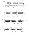
- a sacrificial substrate 10 with a first surface 12 and a second surface 14 is provided.
- One or more recesses 20 are defined in first surface 12 for the receiving of an integrated circuit die.
- Substrate 10 is preferably photo-imagable glass such as, for example, FORTURAN, available from Schott Corp., which is capable of achieving very small etch angles.
- a quartz substrate may be used.
- the diameter and geometry of substrate 10 should be that of the desired end wafer diameter and geometry.
- Recesses 20 are provided with a length and width slightly greater than that of the die which will be incorporated into recesses 20 to minimize the quantity of organic material in the wafer after under-fill.
- the depth of recesses 20 is preferably slightly less than the sum of the thickness of the die and solder ball height to be incorporated into recesses 20 to allow subsequent planarization of first surface 12 as is discussed below.
- Conventional photolithographic techniques as are well known in the art, may be used to create the recesses 20.
- dielectric material 30 such as a polyamide, or vacuum deposited material such as silicon nitride, is applied upon the interior surfaces of recesses 20.
- Dielectric 30 should be a material that is compatible with high temperature processes.
- Alternative methods of depositing dielectric layer 30 include, for example, inkjet printing or pad printing.
- Fig. 3 shows the result of a metalization step applied to dielectric 30 to form conductive pads 40.
- Pads 40 are formed so as to substantially match the I/O pad size and location on the die that will be incorporated into recesses 20. Precise pad placement is important to ensure final die alignment on the neo-wafer.
- one or more integrated circuit die 50 are provided with solder balls 60 applied to the desired I/O pads on die 50.
- Die 50 are aligned on pads 40 within recesses 20 and solder balls 60 reflowed to form an electrically conductive bond between pads 40 and solder balls 60 using conventional flip chip bonding methods.
- first surface 12 is planerized preferably using chemical-mechanical polishing or any other suitable method. Note the flip chip bond and under-fill act as a stress relief during this stage of processing.
- a predetermined portion of second surface 14 is then removed using chemical and/or mechanical lapping so as to expose dielectric 30.
- the result of the planarization and back-thinning of substrate 10 is a neo-wafer with a thickness substantially that of the sum of the die thickness and solder ball diameter.
- vias 70 are then formed in dielectric 30 to provide electrical contact to desired I/O (input/output) pads on each die 50, resulting in a neo-wafer 71 incorporating previously singulated die which is of industry-standard diameter and thickness that can be processed using conventional wafer processing techniques.
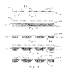
- An alternative embodiment of the invention relates to the formation of high tolerance, high density recesses for the receiving of one or more singulated die in a neo-wafer with desired minimum sidewall thickness is disclosed in Figs 9-17.
- a first layer 72 with an upper surface 74 and a lower surface 76 is provided with the desired neo-wafer diameter.
- First layer 72 is preferably made of glass or similar material.
- Generally die-shaped dielectric structures 80 for the receiving of singulated die are formed on upper surface 74 with a length and width slightly greater than that of the die to be disposed thereon.
- Conductive pads 40 are formed on dielectric structures 80 for the subsequent interconnection of solder balls.
- a base structure 90 is formed by bonding a second layer 100, and a third layer 110, using a suitable adhesive 112 that is capable of withstanding wafer processes.
- Second layer 100 and third layer 110 should be approximately of the same diameter as that of first layer 72.
- Second layer 100 is preferably a glass material and third layer 110 is preferably a silicon material.
- Alternative embodiments include, for example, the use of a first layer of aluminum and a second layer of silicon.
- cavities 120 are formed in third layer 110 at a pitch approximately central to dielectric structures 80 and exposed adhesive 112 is removed.
- Second layer 100 is subsequently etched so as to create very thin sidewall structures 130.
- third layer 110 acts as a sacrificial sidewall carrier and allows the creation of high tolerance sidewalls from second layer 100.
- the height, thickness, length and width of sidewalls 130 are such that the recesses 20 created thereby will receive dielectric structures 80.
- the uppermost sidewall surfaces 140 are precisely aligned and bonded to first layer 72 so that dielectric structures 80 are oriented and disposed within recesses 20 as seen in Fig. 14.
- Fig. 15 shows the step where the remaining portions of third layer 110 and any remaining adhesive have been selectively removed so as to result in a high density, high tolerance sidewall structure 150 for the receiving of singulated die within recesses 20.
- singulated die are flip chip bonded, under-filled within recesses 20, and the bonded first layer 72 and sidewalls 130 planarized, back-thinned and vias exposed to form a neo-wafer 71 of previously singulated die.
- yet a further embodiment includes the elimination of the dielectric layer and for creation of conductive pads directly on the substrate or first layer.
- the substrate or first layer is removed until the pads are exposed.
Landscapes
- Dicing (AREA)
- Wire Bonding (AREA)
- Internal Circuitry In Semiconductor Integrated Circuit Devices (AREA)
Priority Applications (5)
| Application Number | Priority Date | Filing Date | Title |
|---|---|---|---|
| US10/701,783 US6998328B2 (en) | 2002-11-06 | 2003-11-05 | Method for creating neo-wafers from singulated integrated circuit die and a device made according to the method |
| DE200460011025 DE602004011025D1 (de) | 2004-05-12 | 2004-05-12 | Verfahren zur Erstellung einer Halbleiterscheibe aus integrierten Schaltungschips sowie nach diesem Verfahren hergestellte Vorrichtung |
| EP04394026A EP1596433B1 (de) | 2002-11-06 | 2004-05-12 | Verfahren zur Erstellung einer Halbleiterscheibe aus integrierten Schaltungschips sowie nach diesem Verfahren hergestellte Vorrichtung |
| AT04394026T ATE382952T1 (de) | 2002-11-06 | 2004-05-12 | Verfahren zur erstellung einer halbleiterscheibe aus integrierten schaltungschips sowie nach diesem verfahren hergestellte vorrichtung |
| US11/302,480 US20060094240A1 (en) | 2002-11-06 | 2005-12-12 | Neo-wafer device comprised of multiple singulated integrated circuit die |
Applications Claiming Priority (2)
| Application Number | Priority Date | Filing Date | Title |
|---|---|---|---|
| US42402502P | 2002-11-06 | 2002-11-06 | |
| EP04394026A EP1596433B1 (de) | 2002-11-06 | 2004-05-12 | Verfahren zur Erstellung einer Halbleiterscheibe aus integrierten Schaltungschips sowie nach diesem Verfahren hergestellte Vorrichtung |
Publications (2)
| Publication Number | Publication Date |
|---|---|
| EP1596433A1 true EP1596433A1 (de) | 2005-11-16 |
| EP1596433B1 EP1596433B1 (de) | 2008-01-02 |
Family
ID=38670615
Family Applications (1)
| Application Number | Title | Priority Date | Filing Date |
|---|---|---|---|
| EP04394026A Expired - Lifetime EP1596433B1 (de) | 2002-11-06 | 2004-05-12 | Verfahren zur Erstellung einer Halbleiterscheibe aus integrierten Schaltungschips sowie nach diesem Verfahren hergestellte Vorrichtung |
Country Status (3)
| Country | Link |
|---|---|
| US (2) | US6998328B2 (de) |
| EP (1) | EP1596433B1 (de) |
| AT (1) | ATE382952T1 (de) |
Cited By (6)
| Publication number | Priority date | Publication date | Assignee | Title |
|---|---|---|---|---|
| WO2008012481A1 (fr) * | 2006-07-28 | 2008-01-31 | Microcomposants De Haute Sécurité Mhs | Procédé de fabrication d'un circuit intégré encapsulé et circuit intégré encapsulé associé |
| US8159076B2 (en) | 2007-06-07 | 2012-04-17 | Commissariat A L'energie Atomique | Method of producing a via in a reconstituted substrate |
| US8288841B2 (en) | 2009-07-09 | 2012-10-16 | Commissariat à l'énergie atomique et aux énergies alternatives | Handle wafer having viewing windows |
| US8409971B2 (en) | 2007-06-07 | 2013-04-02 | Commissariat A L'energie Atomique | Integrated multicomponent device in a semiconducting die |
| DE102009015722B4 (de) * | 2008-04-18 | 2020-07-09 | Infineon Technologies Ag | Halbleitermodul |
| DE102022113643A1 (de) | 2022-05-31 | 2023-11-30 | Rolls-Royce Deutschland Ltd & Co Kg | Elektrisches Modul |
Families Citing this family (12)
| Publication number | Priority date | Publication date | Assignee | Title |
|---|---|---|---|---|
| US6710454B1 (en) * | 2000-02-16 | 2004-03-23 | Micron Technology, Inc. | Adhesive layer for an electronic apparatus having multiple semiconductor devices |
| US6998328B2 (en) * | 2002-11-06 | 2006-02-14 | Irvine Sensors Corp. | Method for creating neo-wafers from singulated integrated circuit die and a device made according to the method |
| KR100789626B1 (ko) * | 2006-12-27 | 2007-12-27 | 동부일렉트로닉스 주식회사 | 반도체 소자의 제조 방법 |
| DE102007010731A1 (de) * | 2007-02-26 | 2008-08-28 | Würth Elektronik GmbH & Co. KG | Verfahren zum Einbetten von Chips und Leiterplatte |
| DE102012101399B3 (de) * | 2012-02-22 | 2013-08-01 | Chih-hao Chen | Methode zur umweltfreundlichen Bearbeitung von Substraten |
| CN106098630A (zh) * | 2016-08-09 | 2016-11-09 | 中芯长电半导体(江阴)有限公司 | 一种扇出型晶圆级封装方法及封装件 |
| CN106409690B (zh) * | 2016-09-29 | 2019-04-30 | 上海航天电子通讯设备研究所 | 基于激光纳米加工技术的埋置芯片互连方法 |
| US10163693B1 (en) * | 2017-12-21 | 2018-12-25 | Micron Technology, Inc. | Methods for processing semiconductor dice and fabricating assemblies incorporating same |
| US10573547B1 (en) * | 2018-11-05 | 2020-02-25 | Honeywell Federal Manufacturing & Technologies, Llc | Apparatus and method for facilitating planar delayering of integrated circuit die |
| CN110211888A (zh) * | 2019-06-14 | 2019-09-06 | 上海先方半导体有限公司 | 一种嵌入式扇出封装结构及其制造方法 |
| CN110335852A (zh) * | 2019-07-18 | 2019-10-15 | 上海先方半导体有限公司 | 一种扇出封装结构及封装方法 |
| CN112151457A (zh) * | 2020-09-22 | 2020-12-29 | 维沃移动通信有限公司 | 封装结构及其制作方法和电子设备 |
Citations (4)
| Publication number | Priority date | Publication date | Assignee | Title |
|---|---|---|---|---|
| US6117704A (en) * | 1999-03-31 | 2000-09-12 | Irvine Sensors Corporation | Stackable layers containing encapsulated chips |
| US20020192875A1 (en) * | 2001-06-19 | 2002-12-19 | Yusuke Igarashi | Method for fabricating a circuit device |
| US20040046250A1 (en) * | 2002-08-27 | 2004-03-11 | Chua Swee Kwang | Multichip wafer level packages and computing systems incorporating same |
| US6734534B1 (en) * | 2000-08-16 | 2004-05-11 | Intel Corporation | Microelectronic substrate with integrated devices |
Family Cites Families (18)
| Publication number | Priority date | Publication date | Assignee | Title |
|---|---|---|---|---|
| DE4115043A1 (de) * | 1991-05-08 | 1997-07-17 | Gen Electric | Dichtgepackte Verbindungsstruktur, die eine Kammer enthält |
| JP3846094B2 (ja) * | 1998-03-17 | 2006-11-15 | 株式会社デンソー | 半導体装置の製造方法 |
| US6297548B1 (en) * | 1998-06-30 | 2001-10-02 | Micron Technology, Inc. | Stackable ceramic FBGA for high thermal applications |
| US6214640B1 (en) * | 1999-02-10 | 2001-04-10 | Tessera, Inc. | Method of manufacturing a plurality of semiconductor packages |
| US6867499B1 (en) * | 1999-09-30 | 2005-03-15 | Skyworks Solutions, Inc. | Semiconductor packaging |
| JP2001144218A (ja) * | 1999-11-17 | 2001-05-25 | Sony Corp | 半導体装置及び半導体装置の製造方法 |
| WO2001063991A1 (en) * | 2000-02-25 | 2001-08-30 | Ibiden Co., Ltd. | Multilayer printed wiring board and method for producing multilayer printed wiring board |
| US6909178B2 (en) * | 2000-09-06 | 2005-06-21 | Sanyo Electric Co., Ltd. | Semiconductor device and method of manufacturing the same |
| US6709898B1 (en) * | 2000-10-04 | 2004-03-23 | Intel Corporation | Die-in-heat spreader microelectronic package |
| US6507119B2 (en) * | 2000-11-30 | 2003-01-14 | Siliconware Precision Industries Co., Ltd. | Direct-downset flip-chip package assembly and method of fabricating the same |
| US6946366B2 (en) * | 2000-12-05 | 2005-09-20 | Analog Devices, Inc. | Method and device for protecting micro electromechanical systems structures during dicing of a wafer |
| US6541352B2 (en) * | 2001-07-27 | 2003-04-01 | Texas Instruments Incorporated | Semiconductor die with contoured bottom surface and method for making same |
| US6573592B2 (en) * | 2001-08-21 | 2003-06-03 | Micron Technology, Inc. | Semiconductor die packages with standard ball grid array footprint and method for assembling the same |
| US6936917B2 (en) * | 2001-09-26 | 2005-08-30 | Molex Incorporated | Power delivery connector for integrated circuits utilizing integrated capacitors |
| US6797537B2 (en) * | 2001-10-30 | 2004-09-28 | Irvine Sensors Corporation | Method of making stackable layers containing encapsulated integrated circuit chips with one or more overlaying interconnect layers |
| US6762509B2 (en) * | 2001-12-11 | 2004-07-13 | Celerity Research Pte. Ltd. | Flip-chip packaging method that treats an interconnect substrate to control stress created at edges of fill material |
| US6608370B1 (en) * | 2002-01-28 | 2003-08-19 | Motorola, Inc. | Semiconductor wafer having a thin die and tethers and methods of making the same |
| US6998328B2 (en) * | 2002-11-06 | 2006-02-14 | Irvine Sensors Corp. | Method for creating neo-wafers from singulated integrated circuit die and a device made according to the method |
-
2003
- 2003-11-05 US US10/701,783 patent/US6998328B2/en not_active Expired - Fee Related
-
2004
- 2004-05-12 AT AT04394026T patent/ATE382952T1/de not_active IP Right Cessation
- 2004-05-12 EP EP04394026A patent/EP1596433B1/de not_active Expired - Lifetime
-
2005
- 2005-12-12 US US11/302,480 patent/US20060094240A1/en not_active Abandoned
Patent Citations (4)
| Publication number | Priority date | Publication date | Assignee | Title |
|---|---|---|---|---|
| US6117704A (en) * | 1999-03-31 | 2000-09-12 | Irvine Sensors Corporation | Stackable layers containing encapsulated chips |
| US6734534B1 (en) * | 2000-08-16 | 2004-05-11 | Intel Corporation | Microelectronic substrate with integrated devices |
| US20020192875A1 (en) * | 2001-06-19 | 2002-12-19 | Yusuke Igarashi | Method for fabricating a circuit device |
| US20040046250A1 (en) * | 2002-08-27 | 2004-03-11 | Chua Swee Kwang | Multichip wafer level packages and computing systems incorporating same |
Cited By (7)
| Publication number | Priority date | Publication date | Assignee | Title |
|---|---|---|---|---|
| WO2008012481A1 (fr) * | 2006-07-28 | 2008-01-31 | Microcomposants De Haute Sécurité Mhs | Procédé de fabrication d'un circuit intégré encapsulé et circuit intégré encapsulé associé |
| FR2904472A1 (fr) * | 2006-07-28 | 2008-02-01 | Microcomposants De Haute Secur | Procede de fabrication d'un circuit integre encapsule et circuit integre encapsule associe |
| US8159076B2 (en) | 2007-06-07 | 2012-04-17 | Commissariat A L'energie Atomique | Method of producing a via in a reconstituted substrate |
| US8409971B2 (en) | 2007-06-07 | 2013-04-02 | Commissariat A L'energie Atomique | Integrated multicomponent device in a semiconducting die |
| DE102009015722B4 (de) * | 2008-04-18 | 2020-07-09 | Infineon Technologies Ag | Halbleitermodul |
| US8288841B2 (en) | 2009-07-09 | 2012-10-16 | Commissariat à l'énergie atomique et aux énergies alternatives | Handle wafer having viewing windows |
| DE102022113643A1 (de) | 2022-05-31 | 2023-11-30 | Rolls-Royce Deutschland Ltd & Co Kg | Elektrisches Modul |
Also Published As
| Publication number | Publication date |
|---|---|
| US6998328B2 (en) | 2006-02-14 |
| US20040140533A1 (en) | 2004-07-22 |
| EP1596433B1 (de) | 2008-01-02 |
| ATE382952T1 (de) | 2008-01-15 |
| US20060094240A1 (en) | 2006-05-04 |
Similar Documents
| Publication | Publication Date | Title |
|---|---|---|
| US12046482B2 (en) | Microelectronic assemblies | |
| US6998328B2 (en) | Method for creating neo-wafers from singulated integrated circuit die and a device made according to the method | |
| CN110660783B (zh) | 半导体器件封装件和方法 | |
| US8426256B2 (en) | Method of forming stacked-die packages | |
| EP1576649B1 (de) | Stapelbare schichten die eingekapselte integrierte schaltungschips mit einer oder mehreren darüberliegenden verbindungsschichten beinhalten und verfahren zu deren herstellung | |
| KR101347633B1 (ko) | 반도체 패키지의 제조 방법 | |
| CN106206509B (zh) | 电子封装件及其制法与基板结构 | |
| US8021981B2 (en) | Redistribution layers for microfeature workpieces, and associated systems and methods | |
| CN110112115B (zh) | 集成电路封装件及其形成方法 | |
| TWI790702B (zh) | 半導體封裝及製造半導體封裝的方法 | |
| TW201727826A (zh) | 積體晶片的系統及其形成方法 | |
| US11508671B2 (en) | Semiconductor package and manufacturing method thereof | |
| US10325880B2 (en) | Hybrid 3D/2.5D interposer | |
| CN112687634B (zh) | 半导体封装及其制造方法 | |
| CN102270609A (zh) | 用于三维金属互连技术的一般化的器件组装的使用 | |
| TW201906127A (zh) | 半導體封裝及其製造方法 | |
| TWI781101B (zh) | 包括互連結構之半導體系統及裝置封裝 | |
| US7417323B2 (en) | Neo-wafer device and method | |
| US20200303209A1 (en) | Method of fabricating a semiconductor device using an adhesive layer | |
| US10559495B2 (en) | Methods for processing semiconductor dice and fabricating assemblies incorporating same | |
| US12568854B2 (en) | Semiconductor packages having semiconductor blocks surrounding semiconductor device |
Legal Events
| Date | Code | Title | Description |
|---|---|---|---|
| PUAI | Public reference made under article 153(3) epc to a published international application that has entered the european phase |
Free format text: ORIGINAL CODE: 0009012 |
|
| AK | Designated contracting states |
Kind code of ref document: A1 Designated state(s): AT BE BG CH CY CZ DE DK EE ES FI FR GB GR HU IE IT LI LU MC NL PL PT RO SE SI SK TR |
|
| AX | Request for extension of the european patent |
Extension state: AL HR LT LV MK |
|
| 17P | Request for examination filed |
Effective date: 20060322 |
|
| 17Q | First examination report despatched |
Effective date: 20060619 |
|
| AKX | Designation fees paid |
Designated state(s): AT BE BG CH CY CZ DE DK EE ES FI FR GB GR HU IE IT LI LU MC NL PL PT RO SE SI SK TR |
|
| GRAP | Despatch of communication of intention to grant a patent |
Free format text: ORIGINAL CODE: EPIDOSNIGR1 |
|
| GRAS | Grant fee paid |
Free format text: ORIGINAL CODE: EPIDOSNIGR3 |
|
| GRAA | (expected) grant |
Free format text: ORIGINAL CODE: 0009210 |
|
| AK | Designated contracting states |
Kind code of ref document: B1 Designated state(s): AT BE BG CH CY CZ DE DK EE ES FI FR GB GR HU IE IT LI LU MC NL PL PT RO SE SI SK TR |
|
| REG | Reference to a national code |
Ref country code: GB Ref legal event code: FG4D |
|
| REG | Reference to a national code |
Ref country code: IE Ref legal event code: FG4D |
|
| REG | Reference to a national code |
Ref country code: CH Ref legal event code: EP |
|
| REF | Corresponds to: |
Ref document number: 602004011025 Country of ref document: DE Date of ref document: 20080214 Kind code of ref document: P |
|
| PG25 | Lapsed in a contracting state [announced via postgrant information from national office to epo] |
Ref country code: NL Free format text: LAPSE BECAUSE OF FAILURE TO SUBMIT A TRANSLATION OF THE DESCRIPTION OR TO PAY THE FEE WITHIN THE PRESCRIBED TIME-LIMIT Effective date: 20080102 Ref country code: SI Free format text: LAPSE BECAUSE OF FAILURE TO SUBMIT A TRANSLATION OF THE DESCRIPTION OR TO PAY THE FEE WITHIN THE PRESCRIBED TIME-LIMIT Effective date: 20080102 |
|
| NLV1 | Nl: lapsed or annulled due to failure to fulfill the requirements of art. 29p and 29m of the patents act | ||
| PG25 | Lapsed in a contracting state [announced via postgrant information from national office to epo] |
Ref country code: LI Free format text: LAPSE BECAUSE OF FAILURE TO SUBMIT A TRANSLATION OF THE DESCRIPTION OR TO PAY THE FEE WITHIN THE PRESCRIBED TIME-LIMIT Effective date: 20080102 Ref country code: FI Free format text: LAPSE BECAUSE OF FAILURE TO SUBMIT A TRANSLATION OF THE DESCRIPTION OR TO PAY THE FEE WITHIN THE PRESCRIBED TIME-LIMIT Effective date: 20080102 Ref country code: ES Free format text: LAPSE BECAUSE OF FAILURE TO SUBMIT A TRANSLATION OF THE DESCRIPTION OR TO PAY THE FEE WITHIN THE PRESCRIBED TIME-LIMIT Effective date: 20080413 Ref country code: CH Free format text: LAPSE BECAUSE OF FAILURE TO SUBMIT A TRANSLATION OF THE DESCRIPTION OR TO PAY THE FEE WITHIN THE PRESCRIBED TIME-LIMIT Effective date: 20080102 |
|
| REG | Reference to a national code |
Ref country code: CH Ref legal event code: PL |
|
| PG25 | Lapsed in a contracting state [announced via postgrant information from national office to epo] |
Ref country code: BG Free format text: LAPSE BECAUSE OF FAILURE TO SUBMIT A TRANSLATION OF THE DESCRIPTION OR TO PAY THE FEE WITHIN THE PRESCRIBED TIME-LIMIT Effective date: 20080402 Ref country code: AT Free format text: LAPSE BECAUSE OF FAILURE TO SUBMIT A TRANSLATION OF THE DESCRIPTION OR TO PAY THE FEE WITHIN THE PRESCRIBED TIME-LIMIT Effective date: 20080102 |
|
| PG25 | Lapsed in a contracting state [announced via postgrant information from national office to epo] |
Ref country code: PL Free format text: LAPSE BECAUSE OF FAILURE TO SUBMIT A TRANSLATION OF THE DESCRIPTION OR TO PAY THE FEE WITHIN THE PRESCRIBED TIME-LIMIT Effective date: 20080102 Ref country code: BE Free format text: LAPSE BECAUSE OF FAILURE TO SUBMIT A TRANSLATION OF THE DESCRIPTION OR TO PAY THE FEE WITHIN THE PRESCRIBED TIME-LIMIT Effective date: 20080102 Ref country code: PT Free format text: LAPSE BECAUSE OF FAILURE TO SUBMIT A TRANSLATION OF THE DESCRIPTION OR TO PAY THE FEE WITHIN THE PRESCRIBED TIME-LIMIT Effective date: 20080602 |
|
| PG25 | Lapsed in a contracting state [announced via postgrant information from national office to epo] |
Ref country code: CZ Free format text: LAPSE BECAUSE OF FAILURE TO SUBMIT A TRANSLATION OF THE DESCRIPTION OR TO PAY THE FEE WITHIN THE PRESCRIBED TIME-LIMIT Effective date: 20080102 Ref country code: DK Free format text: LAPSE BECAUSE OF FAILURE TO SUBMIT A TRANSLATION OF THE DESCRIPTION OR TO PAY THE FEE WITHIN THE PRESCRIBED TIME-LIMIT Effective date: 20080102 Ref country code: SE Free format text: LAPSE BECAUSE OF FAILURE TO SUBMIT A TRANSLATION OF THE DESCRIPTION OR TO PAY THE FEE WITHIN THE PRESCRIBED TIME-LIMIT Effective date: 20080402 Ref country code: SK Free format text: LAPSE BECAUSE OF FAILURE TO SUBMIT A TRANSLATION OF THE DESCRIPTION OR TO PAY THE FEE WITHIN THE PRESCRIBED TIME-LIMIT Effective date: 20080102 |
|
| PLBE | No opposition filed within time limit |
Free format text: ORIGINAL CODE: 0009261 |
|
| STAA | Information on the status of an ep patent application or granted ep patent |
Free format text: STATUS: NO OPPOSITION FILED WITHIN TIME LIMIT |
|
| PG25 | Lapsed in a contracting state [announced via postgrant information from national office to epo] |
Ref country code: RO Free format text: LAPSE BECAUSE OF FAILURE TO SUBMIT A TRANSLATION OF THE DESCRIPTION OR TO PAY THE FEE WITHIN THE PRESCRIBED TIME-LIMIT Effective date: 20080102 |
|
| 26N | No opposition filed |
Effective date: 20081003 |
|
| PG25 | Lapsed in a contracting state [announced via postgrant information from national office to epo] |
Ref country code: MC Free format text: LAPSE BECAUSE OF NON-PAYMENT OF DUE FEES Effective date: 20080531 |
|
| PG25 | Lapsed in a contracting state [announced via postgrant information from national office to epo] |
Ref country code: DE Free format text: LAPSE BECAUSE OF FAILURE TO SUBMIT A TRANSLATION OF THE DESCRIPTION OR TO PAY THE FEE WITHIN THE PRESCRIBED TIME-LIMIT Effective date: 20080403 Ref country code: EE Free format text: LAPSE BECAUSE OF FAILURE TO SUBMIT A TRANSLATION OF THE DESCRIPTION OR TO PAY THE FEE WITHIN THE PRESCRIBED TIME-LIMIT Effective date: 20080102 |
|
| PGFP | Annual fee paid to national office [announced via postgrant information from national office to epo] |
Ref country code: IE Payment date: 20081111 Year of fee payment: 5 |
|
| PG25 | Lapsed in a contracting state [announced via postgrant information from national office to epo] |
Ref country code: CY Free format text: LAPSE BECAUSE OF FAILURE TO SUBMIT A TRANSLATION OF THE DESCRIPTION OR TO PAY THE FEE WITHIN THE PRESCRIBED TIME-LIMIT Effective date: 20080102 |
|
| PG25 | Lapsed in a contracting state [announced via postgrant information from national office to epo] |
Ref country code: IT Free format text: LAPSE BECAUSE OF FAILURE TO SUBMIT A TRANSLATION OF THE DESCRIPTION OR TO PAY THE FEE WITHIN THE PRESCRIBED TIME-LIMIT Effective date: 20080102 |
|
| REG | Reference to a national code |
Ref country code: GB Ref legal event code: 732E Free format text: REGISTERED BETWEEN 20090917 AND 20090923 |
|
| REG | Reference to a national code |
Ref country code: FR Ref legal event code: TP |
|
| PG25 | Lapsed in a contracting state [announced via postgrant information from national office to epo] |
Ref country code: IE Free format text: LAPSE BECAUSE OF NON-PAYMENT OF DUE FEES Effective date: 20090512 |
|
| PG25 | Lapsed in a contracting state [announced via postgrant information from national office to epo] |
Ref country code: LU Free format text: LAPSE BECAUSE OF NON-PAYMENT OF DUE FEES Effective date: 20080512 Ref country code: HU Free format text: LAPSE BECAUSE OF FAILURE TO SUBMIT A TRANSLATION OF THE DESCRIPTION OR TO PAY THE FEE WITHIN THE PRESCRIBED TIME-LIMIT Effective date: 20080703 |
|
| PG25 | Lapsed in a contracting state [announced via postgrant information from national office to epo] |
Ref country code: TR Free format text: LAPSE BECAUSE OF FAILURE TO SUBMIT A TRANSLATION OF THE DESCRIPTION OR TO PAY THE FEE WITHIN THE PRESCRIBED TIME-LIMIT Effective date: 20080102 |
|
| PG25 | Lapsed in a contracting state [announced via postgrant information from national office to epo] |
Ref country code: GR Free format text: LAPSE BECAUSE OF FAILURE TO SUBMIT A TRANSLATION OF THE DESCRIPTION OR TO PAY THE FEE WITHIN THE PRESCRIBED TIME-LIMIT Effective date: 20080403 |
|
| REG | Reference to a national code |
Ref country code: FR Ref legal event code: PLFP Year of fee payment: 13 |
|
| REG | Reference to a national code |
Ref country code: FR Ref legal event code: PLFP Year of fee payment: 14 |
|
| REG | Reference to a national code |
Ref country code: FR Ref legal event code: PLFP Year of fee payment: 15 |
|
| PGFP | Annual fee paid to national office [announced via postgrant information from national office to epo] |
Ref country code: GB Payment date: 20220421 Year of fee payment: 19 Ref country code: FR Payment date: 20220422 Year of fee payment: 19 |
|
| GBPC | Gb: european patent ceased through non-payment of renewal fee |
Effective date: 20230512 |
|
| PG25 | Lapsed in a contracting state [announced via postgrant information from national office to epo] |
Ref country code: GB Free format text: LAPSE BECAUSE OF NON-PAYMENT OF DUE FEES Effective date: 20230512 |
|
| PG25 | Lapsed in a contracting state [announced via postgrant information from national office to epo] |
Ref country code: FR Free format text: LAPSE BECAUSE OF NON-PAYMENT OF DUE FEES Effective date: 20230531 |