EP1604286B1 - Datenverarbeitungssystem mit einem für die verarbeitung von datenflussanwendungen optimierten cache - Google Patents
Datenverarbeitungssystem mit einem für die verarbeitung von datenflussanwendungen optimierten cache Download PDFInfo
- Publication number
- EP1604286B1 EP1604286B1 EP04714406A EP04714406A EP1604286B1 EP 1604286 B1 EP1604286 B1 EP 1604286B1 EP 04714406 A EP04714406 A EP 04714406A EP 04714406 A EP04714406 A EP 04714406A EP 1604286 B1 EP1604286 B1 EP 1604286B1
- Authority
- EP
- European Patent Office
- Prior art keywords
- cache
- stream
- data
- cache memory
- selecting
- Prior art date
- Legal status (The legal status is an assumption and is not a legal conclusion. Google has not performed a legal analysis and makes no representation as to the accuracy of the status listed.)
- Expired - Lifetime
Links
Images

Classifications
-
- G—PHYSICS
- G06—COMPUTING OR CALCULATING; COUNTING
- G06F—ELECTRIC DIGITAL DATA PROCESSING
- G06F12/00—Accessing, addressing or allocating within memory systems or architectures
- G06F12/02—Addressing or allocation; Relocation
- G06F12/08—Addressing or allocation; Relocation in hierarchically structured memory systems, e.g. virtual memory systems
-
- G—PHYSICS
- G06—COMPUTING OR CALCULATING; COUNTING
- G06F—ELECTRIC DIGITAL DATA PROCESSING
- G06F12/00—Accessing, addressing or allocating within memory systems or architectures
- G06F12/02—Addressing or allocation; Relocation
- G06F12/08—Addressing or allocation; Relocation in hierarchically structured memory systems, e.g. virtual memory systems
- G06F12/0802—Addressing of a memory level in which the access to the desired data or data block requires associative addressing means, e.g. caches
- G06F12/0806—Multiuser, multiprocessor or multiprocessing cache systems
- G06F12/084—Multiuser, multiprocessor or multiprocessing cache systems with a shared cache
Definitions
- the invention relates to a data processing system optimised for processing dataflow applications with tasks and data streams, a semiconductor device for use in a data processing environment optimised for processing dataflow applications with tasks and data streams and a method for indexing a cache memory in a data processing environment optimised for processing dataflow applications with tasks and data streams.
- a first stream might consist of pixel values of an image, that are processed by a first processor to produce a second stream of blocks of DCT (Discrete Cosine Transformation) coefficients of 8x8 blocks of pixels.
- DCT Discrete Cosine Transformation
- a second processor might process the blocks of DCT coefficients to produce a stream of blocks of selected and compressed coefficients for each block of DCT coefficients.
- a number of processors are provided, each capable of performing a particular operation repeatedly, each time using data from a next data object from a stream of data objects and/or producing a next data object in such a stream.
- the streams pass from one processor to another, so that the stream produced by a first processor can be processed by a second processor and so on.
- One mechanism of passing data from a first to a second processor is by writing the data blocks produced by the first processor into the memory.
- the data streams in the network are buffered.
- Each buffer is realised as a FIFO, with precisely one writer and one or more readers. Due to this buffering, the writer and readers do not need to mutually synchronize individual read and write actions on the channel.
- Typical data processing system include a mix of fully programmable processors as well as application specific subsystems dedicated to single application respectively.
- a distributed coprocessor shell is implemented between the coprocessors and the communication network, i.e. the bus and the main memory. It is used to absorb many system-level problems like multitasking, stream synchronisation and data transport. Due to its distributed nature, the shells can be implemented close to the coprocessor, which it is associated to. In each shell all data required for handling the streams incident to tasks being mapped on the coprocessor associated to the shell are stored in the shell's stream table.
- the shells comprise caches in order to reduce data access latency occurring when reading or writing to a memory.
- Data which is required to perform future processing steps are cached i.e. stored in a smaller memory, which is separate from the main memory and is arranged closed to a processor using the stored data.
- a cache is used as an intermediate storage facility.
- the invention is based on the idea to reserve non-overlapping cache locations for each data stream. Therefore, stream information, which is unique to each stream, is used to index the cache memory. Here, this stream information is represented by the stream identification.
- a data processing system optimised for processing dataflow applications with tasks and data streams, where different streams compete for shared cache resources is provided.
- An unambiguous stream identification is associated to each of said data stream.
- Said data processing system comprises at least one processor 12 for processing streaming data, at least one cache memory 200 having a plurality of cache blocks, wherein one of said cache memories 200 is associated to each of said processors 12, and at least one cache controller 300 for controlling said cache memory 200, wherein one of said cache controllers 300 is associated to each of said cache memories 200.
- Said cache controller 300 comprises selecting means 350 for selecting locations for storing elements of a data stream in said cache memory 200 in accordance to said stream identification stream_id. Therefore, the caching of data from different streams is effectively decoupled.
- said selecting means 350 comprises a subset determining means 352 for selecting a set of cache blocks from within said row of cache blocks in said cache memory 200 in accordance with a subset of an Input/Output address of said stream.
- said selecting means 350 comprises a hashing function means 351 for performing a hashing function on said stream identification stream_id to a number which is smaller than the number of cache rows.
- said hashing function means 351 is adapted for performing is a modulo operation.
- said selecting means 350 selects locations for a data stream in said cache memory 200 in accordance to a task identification task_id and/or a port identification port_id associated to said data stream.
- the invention also relates to a semiconductor device for use in a data processing environment optimised for processing dataflow applications with tasks and data streams, where different tasks compete for shared cache resources, wherein an unambiguous stream identification stream_id is associated to each of said data stream.
- Said device comprises a cache memory 200 having a plurality of cache blocks, and a cache controller 300 for controlling said cache memory 200, wherein said cache controller 300 is associated to said cache memory 200.
- Said cache controller 300 comprises selecting means 350 for selecting locations for storing elements of a data stream in said cache memory 200 in accordance to said stream identification stream_id.
- the invention further relates to a method for indexing a cache memory 200 in a data processing environment optimised for processing dataflow applications with tasks and data streams, where different streams compete for shared cache resources.
- Said cache memory 200 comprises a plurality of cache blocks.
- An unambiguous stream identification stream_id is associated to each of said data stream. Locations for storing elements of a data stream in said cache memory 200 are selected in accordance to said stream identification stream_id to distinguish a smaller number of subsets in said cache memory than the potential number of different stream_ids.
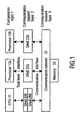
- Fig. 1 shows a processing system for processing streams of data objects according to a preferred embodiment of the invention.
- the system can be divided into different layers, namely a computation layer 1, a communication support layer 2 and a communication network layer 3.
- the computation layer 1 includes a CPU 11, and two processors or processors 12a, 12b. This is merely by way of example, obviously more processors may be included into the system.
- the communication support layer 2 comprises a shell 21 associated to the CPU 11 and shells 22a, 22b associated to the processors 12a, 12b, respectively.
- the communication network layer 3 comprises a communication network 31 and a memory 32.
- the processors 12a, 12b are preferably dedicated processor; each being specialised to perform a limited range of stream processing function. Each processor is arranged to apply the same processing operation repeatedly to successive data objects of a stream.
- the processors 12a, 12b may each perform a different task or function, e.g. variable length decoding, run-length decoding, motion compensation, image scaling or performing a DCT transformation.
- each processor 12a, 12b executes operations on one or more data streams. The operations may involve e.g. receiving a stream and generating another stream or receiving a stream without generating a new stream or generating a stream without receiving a stream or modifying a received stream.
- the processors 12a, 12b are able to process data streams generated by other processors 12b, 12a or by the CPU 11 or even streams that have generated themselves.
- a stream comprises a succession of data objects which are transferred from and to the processors 12a, 12b via said memory 32.
- the shells 22a, 22b comprise a first interface towards the communication network layer being a communication layer. This layer is uniform or generic for all the shells. Furthermore the shells 22a, 22b comprise a second interface towards the processor 12a, 12b to which the shells 22a, 22b are associated to, respectively.
- the second interface is a task-level interface and is customised towards the associated processor 12a, 12b in order to be able to handle the specific needs of said processor 12a, 12b.
- the shells 22a, 22b have a processor-specific interface as the second interface but the overall architecture of the shells is generic and uniform for all processors in order to facilitate the re-use of the shells in the overall system architecture, while allowing the parameterisation and adoption for specific applications.
- the shell 22a, 22b comprise a reading/writing unit for data transport, a synchronisation unit and a task switching unit. These three units communicate with the associated processor on a master/slave basis, wherein the processor acts as master. Accordingly, the respective three unit are initialised by a request from the processor.
- the communication between the processor and the three units is implemented by a request-acknowledge handshake mechanism in order to hand over argument values and wait for the requested values to return. Therefore the communication is blocking, i.e. the respective thread of control waits for their completion.
- the shells 22a, 22b are distributed, such that each can be implemented close to the processor 12a, 12b that it is associated to.
- Each shell locally contains the configuration data for the streams which are incident with tasks mapped on its processor, and locally implements all the control logic to properly handle this data.
- a local stream table may be implemented in the shells 22a, 22b that contains a row of fields for each stream, or in other words, for each access point.
- the shells 22 comprise a data cache for data transport, i.e. read operation and write operations, between the processors 12 and the communication network 31 and the memory 32.
- the implementation of a data cache in the shells 22 provide a transparent translation of data bus widths, a resolvement of alignment restrictions on the global interconnect, i.e. the communication network 31, and a reduction of the number of I/O operations on the global interconnect.
- the shells 22 comprise the cache in the read and write interfaces, however these caches are invisible from the application functionality point of view.
- the caches a play an important role in the decoupling the processor read and write ports from the global interconnect of the communication network 3. These caches have the major influence on the system performance regarding speed, power and area.
- Fig. 2 shows a part of the architecture according to Fig. 1 .
- a processor 12b, the shell 22b, the bus 31 and the memory 32 are shown.
- the shell 22b comprises a cache memory 200 and a cache controller 300 as part of its data transport unit.
- the cache controller 300 comprises a stream table 320 and a selecting means 350.
- the cache memory 200 may be divided into different cache blocks 210.
- a read or write operation i.e. an I/O access
- a task_id When a read or write operation, i.e. an I/O access, is performed by a task on the coprocessor 12b it supplies a task_id and a port_id parameter next to an address indicating from or for which particular task and port it is requesting data.
- the address denotes a location in a stream buffer in shared memory.
- the stream table 320 contains rows of fields for each stream and access points.
- the stream table is indexed with a stream identifier stream_id, which is derived from the task identifier task_id, indicating the task which is currently processed, and a port identifier port_id, indicating the port for which the data is received.
- the port_id has a local scope for each task.
- the first embodiment of the invention is directed to addressing by means of indexing involving a direct address decoding, wherein an entry is determined directly from the decoding. Therefore, said selecting means 350 uses the stream identifier stream_id to select a row of cache blocks in said cache memory 200. A particular cache block from within the selected cache row is indexed through the lower bits of said address supplied by the coprocessor, i.e. the I/O address. Alternatively, the upper bits of the address may be used for indexing.
- the organisation of the cache memory 200 according to this embodiment is done on a direct-mapped basis, i.e. every combination of a stream identifier and an address can only be mapped to a single cache location. Accordingly, the number of cache blocks in a row is restricted to the power of two. In other words, as a column is selected by decoding a number of address bits, this will always expand to a power-of-2 number of columns.
- Fig. 3 shows a conceptual view of the cache organisation according to a second embodiment of the invention, wherein this cache organisation is done on a direct-mapped basis.
- the selecting means from Fig. 2 comprises a hashing function means 351 and a subset determining means 352.
- the stream_id is input to said hashing function means 351, while the I/0 address is input to said subset determining means 352.
- the hashing function means 351 performs a modulo operation over the number of cache rows, in order to translate the stream identifier stream_id to a smaller number of cache rows of said cache memory.
- the subset determining means 352 determines a particular cache column of said cache memory through the lower bits of said address supplied by the coprocessor, i.e.
- the I/O address may be used for indexing.
- the cache row determined by the hashing function means 351 and the cache column determined by said subset determining means 352 a particular cache block can be indexed.
- An actual data word may be located by means of tag matching on the address.
- the port identifier port_id instead of the stream identifier stream_id may be used as input of the hashing function means 351, wherein the hashing function, i.e. a modulo operation over the number of cache rows is performed on the port identifier port_id to render the port_id into a smaller number of cache rows in order to select a cache row.
- the hashing function i.e. a modulo operation over the number of cache rows is performed on the port identifier port_id to render the port_id into a smaller number of cache rows in order to select a cache row.
- the task identifier task_id is used as input to the hashing function means 351, in order to select a cache row.
- the cache indexing scheme according to the invention can be extended to a more general set-associate cache organisation, where the stream_id selects a cache row and the lower bits of the address select a set of cache blocks, while the actual data is further located through tag matching on the address.
Landscapes
- Engineering & Computer Science (AREA)
- Theoretical Computer Science (AREA)
- Physics & Mathematics (AREA)
- General Engineering & Computer Science (AREA)
- General Physics & Mathematics (AREA)
- Memory System Of A Hierarchy Structure (AREA)
- Multi Processors (AREA)
Claims (10)
- Halbleitergerät zur Benutzung in einer Datenverarbeitungsumgebung, welche zum Verarbeiten von Datenflussanwendungen mit Aufgaben und Datenströmung optimiert ist, wobei verschiedene Ströme im Wettbewerb nach Shared-Cache-Ressourcen stehen, wobei eine eindeutige Strom-Identifikation (stream_id) mit jedem der Datenströme assoziiert ist, wobei das Gerät aufweist:einen Cache-Speicher (200), welcher eine Mehrzahl von Cache-Blöcken hat, undeinen Cache-Controller (300) zum Steuern des Cache-Speichers (200), wobei der Cache-Controller (300) mit dem Cache-Speicher (200) assoziiert ist;
dadurch gekennzeichnet, dassder Cache-Controller (300) ein Auswahlmittel (350) zum Auswählen von Orten zum Speichern von Elementen eines Datenstroms in dem Cache-Speicher (200) in Übereinstimmung mit der Strom-Identifikation (stream_id) aufweist. - Gerät nach Anspruch 1, wobei das Auswahlmittel (350) zum Auswählen einer Untermenge von Cache-Blöcken in dem Cache-Speicher (200) in Übereinstimmung mit der Strom-Identifikation (stream_id) ausgebildet ist.
- Gerät nach Anspruch 2, wobei das Auswahlmittel (350) ein Untergruppe-Bestimmungs-Mittel (352) zum Auswählen einer Gruppe von Cache-Blöcken von innerhalb der Untergruppe von Cache-Blöcken in dem Cache-Speicher (200) in Übereinstimmung mit einer Untergruppe einer Eingabe-/Ausgabeadresse des Stroms aufweist.
- Gerät gemäß Anspruch 3, wobei das Untergruppe-Bestimmungs-Mittel (352) zum Auswählen eines Cache-Blocks in Übereinstimmung mit den niedrigeren Bits der Eingabe-/Ausgabeadresse des Stroms ausgebildet ist.
- Gerät nach Anspruch 3, wobei das Untergruppe-Bestimmungs-Mittel (352) zum Auswählen eines Cache-Blocks von innerhalb der Gruppe von Cache-Blöcken mittels Tag-Matchings auf einer Untergruppe der Eingabe-/Ausgabeadressbits ausgebildet ist.
- Gerät nach Anspruch 1, wobei das Auswahlmittel (350) ein Hash-Funktionsmittel (351) zum Durchführen einer Hash-Funktion auf der Stromidentifikation (stream_id) zu einer Zahl, welche kleiner ist als die Zahl von Cache-Zeilen ist, aufweist.
- Gerät nach Anspruch 6, wobei das Hash-Funktionsmittel (351) zum Durchführen einer Modulo-Operation ausgebildet ist.
- Gerät nach Anspruch 1, wobei das Auswahlmittel (350) zum Auswählen von Orten für Elemente eines Datenstroms in dem Cache-Speicher (200) in Übereinstimmung mit einer Aufgabe-Identifikation (task_id) und/oder einer Port-Identifikation (port_id), welche mit dem Datenstrom assoziiert ist, ausgebildet ist.
- Datenverarbeitungssystem, welches ein Halbleitergerät gemäß einem der Ansprüche 1-8 und zumindest einen Prozessor (12) zum Verarbeiten von Stromdaten aufweist, wobei ein Cache-Speicher mit jedem des zumindest einen Prozessors assoziiert ist.
- Verfahren zum Indexieren eines Cache-Speichers (200) in einer Datenverarbeitungsumgebung, welche zum Prozessieren von Datenflussanwendungen mit Aufgaben und Datenströmen optimiert ist, wobei verschiedene Ströme im Wettbewerb nach Shared-Cache-Ressourcen stehen, wobei der Cache-Speicher (200) eine Mehrzahl von Cache-Blöcken aufweist, und wobei eine eindeutige Stromidentifikation (stream_id) mit jedem des Datenstroms assoziiert ist, gekennzeichnet durch den Schritt:Auswählen von Orten zum Speichern von Elementen eines Datenstroms in dem Cache-Speicher (200) in Übereinstimmung mit der Strom-Identifikation (stream_id).
Priority Applications (1)
| Application Number | Priority Date | Filing Date | Title |
|---|---|---|---|
| EP04714406A EP1604286B1 (de) | 2003-03-06 | 2004-02-25 | Datenverarbeitungssystem mit einem für die verarbeitung von datenflussanwendungen optimierten cache |
Applications Claiming Priority (4)
| Application Number | Priority Date | Filing Date | Title |
|---|---|---|---|
| EP03100555 | 2003-03-06 | ||
| EP03100555 | 2003-03-06 | ||
| EP04714406A EP1604286B1 (de) | 2003-03-06 | 2004-02-25 | Datenverarbeitungssystem mit einem für die verarbeitung von datenflussanwendungen optimierten cache |
| PCT/IB2004/050150 WO2004079488A2 (en) | 2003-03-06 | 2004-02-25 | Data processing system with cache optimised for processing dataflow applications |
Publications (2)
| Publication Number | Publication Date |
|---|---|
| EP1604286A2 EP1604286A2 (de) | 2005-12-14 |
| EP1604286B1 true EP1604286B1 (de) | 2010-11-03 |
Family
ID=32946918
Family Applications (1)
| Application Number | Title | Priority Date | Filing Date |
|---|---|---|---|
| EP04714406A Expired - Lifetime EP1604286B1 (de) | 2003-03-06 | 2004-02-25 | Datenverarbeitungssystem mit einem für die verarbeitung von datenflussanwendungen optimierten cache |
Country Status (8)
| Country | Link |
|---|---|
| US (1) | US20070168615A1 (de) |
| EP (1) | EP1604286B1 (de) |
| JP (1) | JP2006520044A (de) |
| KR (1) | KR20050116811A (de) |
| CN (1) | CN100547567C (de) |
| AT (1) | ATE487182T1 (de) |
| DE (1) | DE602004029870D1 (de) |
| WO (1) | WO2004079488A2 (de) |
Families Citing this family (11)
| Publication number | Priority date | Publication date | Assignee | Title |
|---|---|---|---|---|
| EP0563708B1 (de) | 1992-03-19 | 2000-06-21 | Fuji Photo Film Co., Ltd. | Verfahren zur Herstellung einer photographischen Silberhalogenidemulsion |
| US7111124B2 (en) * | 2002-03-12 | 2006-09-19 | Intel Corporation | Set partitioning for cache memories |
| US7523319B2 (en) * | 2005-11-16 | 2009-04-21 | Lenovo (Singapore) Pte. Ltd. | System and method for tracking changed LBAs on disk drive |
| US8130841B2 (en) * | 2005-12-29 | 2012-03-06 | Harris Corporation | Method and apparatus for compression of a video signal |
| US7876328B2 (en) * | 2007-02-08 | 2011-01-25 | Via Technologies, Inc. | Managing multiple contexts in a decentralized graphics processing unit |
| US9076239B2 (en) | 2009-04-30 | 2015-07-07 | Stmicroelectronics S.R.L. | Method and systems for thumbnail generation, and corresponding computer program product |
| JP5800347B2 (ja) * | 2010-03-31 | 2015-10-28 | 日本電気株式会社 | 情報処理装置及びデータアクセス方法 |
| FR2958765B1 (fr) * | 2010-04-09 | 2012-04-13 | Commissariat Energie Atomique | Memoire cache segmentee. |
| CN103729315B (zh) | 2012-10-15 | 2016-12-21 | 华为技术有限公司 | 一种地址压缩、解压缩的方法、压缩器和解压缩器 |
| US10073786B2 (en) * | 2015-05-28 | 2018-09-11 | Micron Technology, Inc. | Apparatuses and methods for compute enabled cache |
| KR101967857B1 (ko) * | 2017-09-12 | 2019-08-19 | 전자부품연구원 | 다중 캐시 메모리를 구비한 지능형 반도체 장치 및 지능형 반도체 장치에서의 메모리 접근 방법 |
Family Cites Families (21)
| Publication number | Priority date | Publication date | Assignee | Title |
|---|---|---|---|---|
| JPS62144257A (ja) * | 1985-12-19 | 1987-06-27 | Mitsubishi Electric Corp | キヤツシユメモリ |
| JPS6466760A (en) * | 1987-09-08 | 1989-03-13 | Fujitsu Ltd | Disk cache control system |
| JPS6466761A (en) * | 1987-09-08 | 1989-03-13 | Fujitsu Ltd | Disk cache control system |
| JP2846697B2 (ja) * | 1990-02-13 | 1999-01-13 | 三洋電機株式会社 | キャッシュメモリ制御装置 |
| JPH04100158A (ja) * | 1990-08-18 | 1992-04-02 | Pfu Ltd | キャッシュ制御方式 |
| JPH0571948U (ja) * | 1992-03-04 | 1993-09-28 | 横河電機株式会社 | キャッシュ制御装置 |
| JPH06160828A (ja) * | 1992-11-26 | 1994-06-07 | Sharp Corp | 平板の貼合せ方法 |
| US5511212A (en) * | 1993-06-10 | 1996-04-23 | Rockoff; Todd E. | Multi-clock SIMD computer and instruction-cache-enhancement thereof |
| DE69826539D1 (de) * | 1997-01-30 | 2004-11-04 | Sgs Thomson Microelectronics | Cachespeichersystem |
| TW501011B (en) * | 1998-05-08 | 2002-09-01 | Koninkl Philips Electronics Nv | Data processing circuit with cache memory |
| US6389513B1 (en) * | 1998-05-13 | 2002-05-14 | International Business Machines Corporation | Disk block cache management for a distributed shared memory computer system |
| US6349363B2 (en) * | 1998-12-08 | 2002-02-19 | Intel Corporation | Multi-section cache with different attributes for each section |
| JP2000339220A (ja) * | 1999-05-27 | 2000-12-08 | Nippon Telegr & Teleph Corp <Ntt> | キャッシュブロック予約方法およびキャッシュブロック予約機能付きコンピュータシステム |
| US6360299B1 (en) * | 1999-06-30 | 2002-03-19 | International Business Machines Corporation | Extended cache state with prefetched stream ID information |
| JP2001282617A (ja) * | 2000-03-27 | 2001-10-12 | Internatl Business Mach Corp <Ibm> | 共有されたキャッシュを動的に区分するための方法及びシステム |
| US6567900B1 (en) * | 2000-08-31 | 2003-05-20 | Hewlett-Packard Development Company, L.P. | Efficient address interleaving with simultaneous multiple locality options |
| US6487643B1 (en) * | 2000-09-29 | 2002-11-26 | Intel Corporation | Method and apparatus for preventing starvation in a multi-node architecture |
| US6754776B2 (en) * | 2001-05-17 | 2004-06-22 | Fujitsu Limited | Method and system for logical partitioning of cache memory structures in a partitoned computer system |
| US6965982B2 (en) * | 2001-06-29 | 2005-11-15 | International Business Machines Corporation | Multithreaded processor efficiency by pre-fetching instructions for a scheduled thread |
| US6883084B1 (en) * | 2001-07-25 | 2005-04-19 | University Of New Mexico | Reconfigurable data path processor |
| US6820170B1 (en) * | 2002-06-24 | 2004-11-16 | Applied Micro Circuits Corporation | Context based cache indexing |
-
2004
- 2004-02-25 JP JP2006506643A patent/JP2006520044A/ja active Pending
- 2004-02-25 AT AT04714406T patent/ATE487182T1/de not_active IP Right Cessation
- 2004-02-25 CN CNB200480005890XA patent/CN100547567C/zh not_active Expired - Fee Related
- 2004-02-25 DE DE602004029870T patent/DE602004029870D1/de not_active Expired - Lifetime
- 2004-02-25 US US10/547,595 patent/US20070168615A1/en not_active Abandoned
- 2004-02-25 KR KR1020057016628A patent/KR20050116811A/ko not_active Ceased
- 2004-02-25 EP EP04714406A patent/EP1604286B1/de not_active Expired - Lifetime
- 2004-02-25 WO PCT/IB2004/050150 patent/WO2004079488A2/en not_active Ceased
Also Published As
| Publication number | Publication date |
|---|---|
| WO2004079488A2 (en) | 2004-09-16 |
| CN100547567C (zh) | 2009-10-07 |
| KR20050116811A (ko) | 2005-12-13 |
| JP2006520044A (ja) | 2006-08-31 |
| CN1757017A (zh) | 2006-04-05 |
| EP1604286A2 (de) | 2005-12-14 |
| US20070168615A1 (en) | 2007-07-19 |
| DE602004029870D1 (de) | 2010-12-16 |
| WO2004079488A3 (en) | 2005-07-28 |
| ATE487182T1 (de) | 2010-11-15 |
Similar Documents
| Publication | Publication Date | Title |
|---|---|---|
| US10824341B2 (en) | Flash-based accelerator and computing device including the same | |
| US20120221785A1 (en) | Polymorphic Stacked DRAM Memory Architecture | |
| US20080285652A1 (en) | Apparatus and methods for optimization of image and motion picture memory access | |
| US11599483B2 (en) | Dedicated cache-related block transfer in a memory system | |
| US20050097280A1 (en) | System and method for sharing memory by Heterogen ous processors | |
| US20050268048A1 (en) | System and method for using a plurality of heterogeneous processors in a common computer system | |
| US9086920B2 (en) | Device for managing data buffers in a memory space divided into a plurality of memory elements | |
| US7630388B2 (en) | Software defined FIFO memory for storing a set of data from a stream of source data | |
| CN1757018B (zh) | 具有预取装置的数据处理系统、数据预取方法 | |
| US20060080398A1 (en) | Direct access of cache lock set data without backing memory | |
| US9697111B2 (en) | Method of managing dynamic memory reallocation and device performing the method | |
| CN104737143A (zh) | 存储器访问控制模块以及相关方法 | |
| US12229673B2 (en) | Sparsity-aware datastore for inference processing in deep neural network architectures | |
| US8566532B2 (en) | Management of multipurpose command queues in a multilevel cache hierarchy | |
| US20070168615A1 (en) | Data processing system with cache optimised for processing dataflow applications | |
| KR20150080568A (ko) | 이미지 메모리 액세스 최적화 | |
| JP2006323824A (ja) | プロセッサシステム内においてスタックを分離して管理する方法および装置 | |
| WO2024260231A1 (zh) | 缓存结构和电子设备 | |
| Vaithianathan | Memory hierarchy optimization strategies for HighPerformance computing architectures | |
| US20110066813A1 (en) | Method And System For Local Data Sharing | |
| CN114116533A (zh) | 利用共享存储器存储数据的方法 | |
| US10620958B1 (en) | Crossbar between clients and a cache | |
| EP1449087A1 (de) | Bandbreitenverbesserung für einrichtungen ohne cache-speicherung | |
| US20070028071A1 (en) | Memory device | |
| KR960005394B1 (ko) | 멀티 프로세서 시스템 |
Legal Events
| Date | Code | Title | Description |
|---|---|---|---|
| PUAI | Public reference made under article 153(3) epc to a published international application that has entered the european phase |
Free format text: ORIGINAL CODE: 0009012 |
|
| AK | Designated contracting states |
Kind code of ref document: A2 Designated state(s): AT BE BG CH CY CZ DE DK EE ES FI FR GB GR HU IE IT LI LU MC NL PT RO SE SI SK TR |
|
| AX | Request for extension of the european patent |
Extension state: AL LT LV MK |
|
| 17P | Request for examination filed |
Effective date: 20060130 |
|
| RBV | Designated contracting states (corrected) |
Designated state(s): AT BE BG CH CY CZ DE DK EE ES FI FR GB GR HU IE IT LI LU MC NL PT RO SE SI SK TR |
|
| DAX | Request for extension of the european patent (deleted) | ||
| RAP1 | Party data changed (applicant data changed or rights of an application transferred) |
Owner name: NXP B.V. |
|
| 17Q | First examination report despatched |
Effective date: 20081028 |
|
| GRAP | Despatch of communication of intention to grant a patent |
Free format text: ORIGINAL CODE: EPIDOSNIGR1 |
|
| GRAS | Grant fee paid |
Free format text: ORIGINAL CODE: EPIDOSNIGR3 |
|
| GRAA | (expected) grant |
Free format text: ORIGINAL CODE: 0009210 |
|
| AK | Designated contracting states |
Kind code of ref document: B1 Designated state(s): AT BE BG CH CY CZ DE DK EE ES FI FR GB GR HU IE IT LI LU MC NL PT RO SE SI SK TR |
|
| REG | Reference to a national code |
Ref country code: GB Ref legal event code: FG4D |
|
| REG | Reference to a national code |
Ref country code: CH Ref legal event code: EP |
|
| REG | Reference to a national code |
Ref country code: IE Ref legal event code: FG4D |
|
| REF | Corresponds to: |
Ref document number: 602004029870 Country of ref document: DE Date of ref document: 20101216 Kind code of ref document: P |
|
| REG | Reference to a national code |
Ref country code: NL Ref legal event code: VDEP Effective date: 20101103 |
|
| PG25 | Lapsed in a contracting state [announced via postgrant information from national office to epo] |
Ref country code: PT Free format text: LAPSE BECAUSE OF FAILURE TO SUBMIT A TRANSLATION OF THE DESCRIPTION OR TO PAY THE FEE WITHIN THE PRESCRIBED TIME-LIMIT Effective date: 20110303 Ref country code: SI Free format text: LAPSE BECAUSE OF FAILURE TO SUBMIT A TRANSLATION OF THE DESCRIPTION OR TO PAY THE FEE WITHIN THE PRESCRIBED TIME-LIMIT Effective date: 20101103 Ref country code: SE Free format text: LAPSE BECAUSE OF FAILURE TO SUBMIT A TRANSLATION OF THE DESCRIPTION OR TO PAY THE FEE WITHIN THE PRESCRIBED TIME-LIMIT Effective date: 20101103 Ref country code: BG Free format text: LAPSE BECAUSE OF FAILURE TO SUBMIT A TRANSLATION OF THE DESCRIPTION OR TO PAY THE FEE WITHIN THE PRESCRIBED TIME-LIMIT Effective date: 20110203 Ref country code: NL Free format text: LAPSE BECAUSE OF FAILURE TO SUBMIT A TRANSLATION OF THE DESCRIPTION OR TO PAY THE FEE WITHIN THE PRESCRIBED TIME-LIMIT Effective date: 20101103 Ref country code: FI Free format text: LAPSE BECAUSE OF FAILURE TO SUBMIT A TRANSLATION OF THE DESCRIPTION OR TO PAY THE FEE WITHIN THE PRESCRIBED TIME-LIMIT Effective date: 20101103 Ref country code: AT Free format text: LAPSE BECAUSE OF FAILURE TO SUBMIT A TRANSLATION OF THE DESCRIPTION OR TO PAY THE FEE WITHIN THE PRESCRIBED TIME-LIMIT Effective date: 20101103 |
|
| PGFP | Annual fee paid to national office [announced via postgrant information from national office to epo] |
Ref country code: DE Payment date: 20110223 Year of fee payment: 8 Ref country code: FR Payment date: 20110218 Year of fee payment: 8 |
|
| PG25 | Lapsed in a contracting state [announced via postgrant information from national office to epo] |
Ref country code: GR Free format text: LAPSE BECAUSE OF FAILURE TO SUBMIT A TRANSLATION OF THE DESCRIPTION OR TO PAY THE FEE WITHIN THE PRESCRIBED TIME-LIMIT Effective date: 20110204 |
|
| PG25 | Lapsed in a contracting state [announced via postgrant information from national office to epo] |
Ref country code: EE Free format text: LAPSE BECAUSE OF FAILURE TO SUBMIT A TRANSLATION OF THE DESCRIPTION OR TO PAY THE FEE WITHIN THE PRESCRIBED TIME-LIMIT Effective date: 20101103 Ref country code: BE Free format text: LAPSE BECAUSE OF FAILURE TO SUBMIT A TRANSLATION OF THE DESCRIPTION OR TO PAY THE FEE WITHIN THE PRESCRIBED TIME-LIMIT Effective date: 20101103 Ref country code: ES Free format text: LAPSE BECAUSE OF FAILURE TO SUBMIT A TRANSLATION OF THE DESCRIPTION OR TO PAY THE FEE WITHIN THE PRESCRIBED TIME-LIMIT Effective date: 20110214 Ref country code: CZ Free format text: LAPSE BECAUSE OF FAILURE TO SUBMIT A TRANSLATION OF THE DESCRIPTION OR TO PAY THE FEE WITHIN THE PRESCRIBED TIME-LIMIT Effective date: 20101103 |
|
| PGFP | Annual fee paid to national office [announced via postgrant information from national office to epo] |
Ref country code: GB Payment date: 20110223 Year of fee payment: 8 |
|
| PG25 | Lapsed in a contracting state [announced via postgrant information from national office to epo] |
Ref country code: SK Free format text: LAPSE BECAUSE OF FAILURE TO SUBMIT A TRANSLATION OF THE DESCRIPTION OR TO PAY THE FEE WITHIN THE PRESCRIBED TIME-LIMIT Effective date: 20101103 Ref country code: DK Free format text: LAPSE BECAUSE OF FAILURE TO SUBMIT A TRANSLATION OF THE DESCRIPTION OR TO PAY THE FEE WITHIN THE PRESCRIBED TIME-LIMIT Effective date: 20101103 Ref country code: RO Free format text: LAPSE BECAUSE OF FAILURE TO SUBMIT A TRANSLATION OF THE DESCRIPTION OR TO PAY THE FEE WITHIN THE PRESCRIBED TIME-LIMIT Effective date: 20101103 |
|
| PLBE | No opposition filed within time limit |
Free format text: ORIGINAL CODE: 0009261 |
|
| STAA | Information on the status of an ep patent application or granted ep patent |
Free format text: STATUS: NO OPPOSITION FILED WITHIN TIME LIMIT |
|
| PG25 | Lapsed in a contracting state [announced via postgrant information from national office to epo] |
Ref country code: MC Free format text: LAPSE BECAUSE OF NON-PAYMENT OF DUE FEES Effective date: 20110228 |
|
| REG | Reference to a national code |
Ref country code: CH Ref legal event code: PL |
|
| 26N | No opposition filed |
Effective date: 20110804 |
|
| PG25 | Lapsed in a contracting state [announced via postgrant information from national office to epo] |
Ref country code: CH Free format text: LAPSE BECAUSE OF NON-PAYMENT OF DUE FEES Effective date: 20110228 Ref country code: LI Free format text: LAPSE BECAUSE OF NON-PAYMENT OF DUE FEES Effective date: 20110228 |
|
| REG | Reference to a national code |
Ref country code: IE Ref legal event code: MM4A |
|
| REG | Reference to a national code |
Ref country code: DE Ref legal event code: R097 Ref document number: 602004029870 Country of ref document: DE Effective date: 20110804 |
|
| PG25 | Lapsed in a contracting state [announced via postgrant information from national office to epo] |
Ref country code: IT Free format text: LAPSE BECAUSE OF FAILURE TO SUBMIT A TRANSLATION OF THE DESCRIPTION OR TO PAY THE FEE WITHIN THE PRESCRIBED TIME-LIMIT Effective date: 20101103 |
|
| PG25 | Lapsed in a contracting state [announced via postgrant information from national office to epo] |
Ref country code: IE Free format text: LAPSE BECAUSE OF NON-PAYMENT OF DUE FEES Effective date: 20110225 |
|
| GBPC | Gb: european patent ceased through non-payment of renewal fee |
Effective date: 20120225 |
|
| REG | Reference to a national code |
Ref country code: FR Ref legal event code: ST Effective date: 20121031 |
|
| REG | Reference to a national code |
Ref country code: DE Ref legal event code: R119 Ref document number: 602004029870 Country of ref document: DE Effective date: 20120901 |
|
| PG25 | Lapsed in a contracting state [announced via postgrant information from national office to epo] |
Ref country code: FR Free format text: LAPSE BECAUSE OF NON-PAYMENT OF DUE FEES Effective date: 20120229 Ref country code: GB Free format text: LAPSE BECAUSE OF NON-PAYMENT OF DUE FEES Effective date: 20120225 |
|
| PG25 | Lapsed in a contracting state [announced via postgrant information from national office to epo] |
Ref country code: LU Free format text: LAPSE BECAUSE OF NON-PAYMENT OF DUE FEES Effective date: 20110225 Ref country code: CY Free format text: LAPSE BECAUSE OF FAILURE TO SUBMIT A TRANSLATION OF THE DESCRIPTION OR TO PAY THE FEE WITHIN THE PRESCRIBED TIME-LIMIT Effective date: 20101103 |
|
| PG25 | Lapsed in a contracting state [announced via postgrant information from national office to epo] |
Ref country code: DE Free format text: LAPSE BECAUSE OF NON-PAYMENT OF DUE FEES Effective date: 20120901 |
|
| PG25 | Lapsed in a contracting state [announced via postgrant information from national office to epo] |
Ref country code: TR Free format text: LAPSE BECAUSE OF FAILURE TO SUBMIT A TRANSLATION OF THE DESCRIPTION OR TO PAY THE FEE WITHIN THE PRESCRIBED TIME-LIMIT Effective date: 20101103 |
|
| PG25 | Lapsed in a contracting state [announced via postgrant information from national office to epo] |
Ref country code: HU Free format text: LAPSE BECAUSE OF FAILURE TO SUBMIT A TRANSLATION OF THE DESCRIPTION OR TO PAY THE FEE WITHIN THE PRESCRIBED TIME-LIMIT Effective date: 20101103 |