EP1610341A2 - Magnetisches Speicherzellenfeld mit benachbarter gekoppelter weichmagnetischer Schicht - Google Patents
Magnetisches Speicherzellenfeld mit benachbarter gekoppelter weichmagnetischer Schicht Download PDFInfo
- Publication number
- EP1610341A2 EP1610341A2 EP05392008A EP05392008A EP1610341A2 EP 1610341 A2 EP1610341 A2 EP 1610341A2 EP 05392008 A EP05392008 A EP 05392008A EP 05392008 A EP05392008 A EP 05392008A EP 1610341 A2 EP1610341 A2 EP 1610341A2
- Authority
- EP
- European Patent Office
- Prior art keywords
- layer
- cell
- bit line
- thickness
- free layer
- Prior art date
- Legal status (The legal status is an assumption and is not a legal conclusion. Google has not performed a legal analysis and makes no representation as to the accuracy of the status listed.)
- Granted
Links
Images
Classifications
-
- G—PHYSICS
- G11—INFORMATION STORAGE
- G11C—STATIC STORES
- G11C11/00—Digital stores characterised by the use of particular electric or magnetic storage elements; Storage elements therefor
- G11C11/02—Digital stores characterised by the use of particular electric or magnetic storage elements; Storage elements therefor using magnetic elements
- G11C11/16—Digital stores characterised by the use of particular electric or magnetic storage elements; Storage elements therefor using magnetic elements using elements in which the storage effect is based on magnetic spin effect
- G11C11/165—Auxiliary circuits
- G11C11/1653—Address circuits or decoders
- G11C11/1655—Bit-line or column circuits
-
- G—PHYSICS
- G11—INFORMATION STORAGE
- G11C—STATIC STORES
- G11C11/00—Digital stores characterised by the use of particular electric or magnetic storage elements; Storage elements therefor
- G11C11/02—Digital stores characterised by the use of particular electric or magnetic storage elements; Storage elements therefor using magnetic elements
- G11C11/16—Digital stores characterised by the use of particular electric or magnetic storage elements; Storage elements therefor using magnetic elements using elements in which the storage effect is based on magnetic spin effect
- G11C11/161—Digital stores characterised by the use of particular electric or magnetic storage elements; Storage elements therefor using magnetic elements using elements in which the storage effect is based on magnetic spin effect details concerning the memory cell structure, e.g. the layers of the ferromagnetic memory cell
-
- G—PHYSICS
- G11—INFORMATION STORAGE
- G11C—STATIC STORES
- G11C11/00—Digital stores characterised by the use of particular electric or magnetic storage elements; Storage elements therefor
- G11C11/02—Digital stores characterised by the use of particular electric or magnetic storage elements; Storage elements therefor using magnetic elements
- G11C11/16—Digital stores characterised by the use of particular electric or magnetic storage elements; Storage elements therefor using magnetic elements using elements in which the storage effect is based on magnetic spin effect
- G11C11/165—Auxiliary circuits
- G11C11/1653—Address circuits or decoders
- G11C11/1657—Word-line or row circuits
-
- G—PHYSICS
- G11—INFORMATION STORAGE
- G11C—STATIC STORES
- G11C11/00—Digital stores characterised by the use of particular electric or magnetic storage elements; Storage elements therefor
- G11C11/02—Digital stores characterised by the use of particular electric or magnetic storage elements; Storage elements therefor using magnetic elements
- G11C11/16—Digital stores characterised by the use of particular electric or magnetic storage elements; Storage elements therefor using magnetic elements using elements in which the storage effect is based on magnetic spin effect
- G11C11/165—Auxiliary circuits
- G11C11/1659—Cell access
-
- G—PHYSICS
- G11—INFORMATION STORAGE
- G11C—STATIC STORES
- G11C11/00—Digital stores characterised by the use of particular electric or magnetic storage elements; Storage elements therefor
- G11C11/02—Digital stores characterised by the use of particular electric or magnetic storage elements; Storage elements therefor using magnetic elements
- G11C11/16—Digital stores characterised by the use of particular electric or magnetic storage elements; Storage elements therefor using magnetic elements using elements in which the storage effect is based on magnetic spin effect
- G11C11/165—Auxiliary circuits
- G11C11/1675—Writing or programming circuits or methods
-
- H—ELECTRICITY
- H10—SEMICONDUCTOR DEVICES; ELECTRIC SOLID-STATE DEVICES NOT OTHERWISE PROVIDED FOR
- H10N—ELECTRIC SOLID-STATE DEVICES NOT OTHERWISE PROVIDED FOR
- H10N50/00—Galvanomagnetic devices
- H10N50/10—Magnetoresistive devices
Definitions
- This invention relates to the design and fabrication of magnetic tunnel junctions (MTJ) as memory storage devices, particularly to a design wherein a soft-magnetic adjacent layer is included as part of a composite bit line.
- MTJ magnetic tunnel junctions
- the magnetic tunnel junction basically comprises two electrodes, which are layers of ferromagnetic material, separated by a tunnel barrier layer, which is a thin layer of insulating material.
- the tunnel barrier layer must be sufficiently thin so that there is a probability for charge carriers (typically electrons) to cross the layer by means of quantum mechanical tunneling.
- the tunneling probability is spin dependent, however, depending on the availability of tunneling states with different electron spin orientations.
- the overall tunneling current will depend on the number of spin-up vs. spin-down electrons, which in turn depends on the orientation of the electron spin relative to the magnetization direction of the ferromagnetic layers. Thus, if these magnetization directions are varied for a given applied voltage, the tunneling current will also vary as a function of the relative directions.
- sensing the change of tunneling current for a fixed potential can enable a determination of the relative magnetization directions of the two ferromagnetic layers that comprise it. Equivalently, the resistance of the MTJ can be measured, since different relative magnetization directions will produce different resistances.
- an MTJ as an information storage device requires that the magnetization of at least one of its ferromagnetic layers can be varied relative to the other and also that changes in the relative directions can be sensed by means of variations in the tunneling current or, equivalently, the junction resistance.
- the MTJ need only be capable of having its magnetizations put into parallel (low resistance) or antiparallel (high resistance) configurations (writing data) and that these two configurations can be sensed by tunneling current variations or resistance variations (reading data).
- the free ferromagnetic layer can be modeled as having a magnetization which is free to rotate but which energetically prefers to align in either direction along its easy axis (the direction of magnetic crystalline anisotropy).
- the magnetization of the fixed layer may be thought of as being permanently aligned in its easy axis direction.
- the junction will have its maximum resistance, when the free layer is aligned with the fixed layer, the minimum resistance is present.
- the MTJ devices are located at the intersection of current carrying lines called word lines and bit lines. When both lines are activated, the device is written upon, ie, the magnetization direction of its free layer is changed.
- Such an MTJ device is provided by Gallagher et al. (U. S. Patent No. 5,650,958), who teach the formation of an MTJ device with a pinned ferromagnetic layer whose magnetization is in the plane of the layer but not free to rotate, together with a free magnetic layer whose magnetization is free to rotate relative to that of the pinned layer, wherein the two layers are separated by an insulating tunnel barrier layer.
- Some degree of anisotropy is necessary if an MTJ cell is to be capable of maintaining a magnetization direction and, thereby, to effectively store data even when write currents are zero.
- the technology has sought to provide a degree of magnetic anisotropy by forming cells in a wide variety of shapes (eg. rectangles, diamonds, ellipses, etc.), so that the lack of inherent crystalline anisotropy is countered by a shape anisotropy.
- this form of anisotropy brings with it its own problems.
- a particularly troublesome shape-related problem in MTJ devices results from non-uniform and uncontrollable edge-fields produced by shape anisotropy (a property of non-circular samples).
- Chen et al. (U. S. Patent No. 5,966,323) teaches a MTJ MRAM cell that can be switched with a low applied field by forming magnetic layers coupled in antiparallel directions so that the cell, as a whole, has no magnetic moment.
- Inomata et al. (U. S. Patent No. 6,611,405 B1) provide a multi-layer, multi-tunnel junction MRAM device in which a current of spin-polarized electrons flows through the device while bit and word lines also carry current. The arrangement allows an easier reorientation of the magnetic moments with lower currents.
- Engel et al. (U. S. Patent No. 6,531,723 B1) teach the formation of an MRAM cell in which the free layer is a multi-layered laminate of antiferromagnetically coupled layers. Increasing the number of layers in the laminate increases the magnetic switching volume of the cell so that the energy barrier that must be exceeded in order to inadvertently switch the magnetization direction is increased.
- This invention addresses the problem of the high current required to reorient the magnetization of the free layer in ultra-small MRAM cells wherein the super-paramagnetic behavior requires thick free layers. It does so by forming a composite bit line with an adjacent soft magnetic layer that concentrates the magnetic field at the free layer.
- a first object of this invention is to provide an MTJ MRAM cell and an array of such cells, which is thermally stable against fluctuations of the magnetization of the free layer.
- a second object of this invention is to provide such an MRAM cell and array of such cells, in which the switching current is not excessive.
- a third object of this invention is to provide an MRAM cell in which thermal stability can be achieved with a circular or low aspect ratio elliptical cross-section, the patterning of such shapes being easier to scale and less subject to shape variation and consequent uncontrollable shape anisotropies.
- the soft magnetic material of the SAL can be Ni, Fe, Co and their alloys, while the conducting material can be high conductivity materials such as Cu, Au, Al, Ag, CuAg, Ta, Cr, NiCr, NiFeCr, Ru, Rh and their multi-layers and alloys.
- the switching current flows substantially through the high conductivity material, so the SAL can be made very thin.
- the SAL concentrates the magnetic field produced by the current in the bit line and the proximity of the SAL to the free layer makes the enhanced field extremely effective in switching as a result of magnetostatic coupling between the SAL and the free layer.
- the magnetization (30) of the SAL beneath a particular circular MRAM cell (10) tends to line up along the bit line (20) current direction (40) when the write current in the bit line is in the direction of the solid arrows (x-direction).
- the magnetization of the cell free layer (60) (shown displaced from its position above the bit line for clarity) is perpendicular to the bit line (y-direction).
- the cell has no shape anisotropy because of its circular cross-section, but there is an interaction anisotropy due to magnetostatic interaction with the SAL beneath the cell.
- This interaction anisotropy is controlled by M s t (product of magnetic moment and thickness) of the free layer and the SAL and the spacing between them.
- M s t product of magnetic moment and thickness
- This interaction anisotropy can be precisely controlled by the fabrication process.
- the word line write current generates a magnetic field in the direction of the bit line (+x) which will line up the magnetization of the SAL under the free layer in that same direction.
- the magnetization of the SAL will rotate the magnetization of the free layer towards the +x direction, weakening the interaction anisotropy.
- a small bit line current will rotate the magnetizations of the SAL and free layer in opposite directions, since they are respectively below and above the current. Removing the word line write current and then the bit line current in sequence will leave the magnetizations of the free layer and SAL layer coupled by their mutual dipole interaction with the magnetization of the free layer controlled by the direction of the bit line current.
- K in the interaction anisotropy
- K in the interaction anisotropy
- K in is proportional to: K in ⁇ M s (SAL) x M s (free) x t SAL x a 2 x r -3
- a is the diameter of the cell
- r is the distance between the free layer and the cell
- M s is the magnetic moment.
- the extreme sensitivity to r shows that the bit line needs to be thin and close to the free layer. Also, because it is the bit line current that is responsible for the switching, the current must be substantially in the highly conductive bit line layer.
- the deposition process induced anisotropy and/or the shape induced anisotropy can be set along the bit line direction (x), since these anisotropies subtract from the interaction anisotropy.
- an alternative design to enhance the word line write current field efficiency would be to add a magnetic cladding layer over the word line on the side away from the cell.
- the preferred embodiment of the present invention teaches a method of forming an MTJ MRAM cell of substantially circular cross-section or an MRAM array of such cells, in which the required switching current in the bit line can be reduced by the addition of a thin adjacent soft magnetic layer beneath the bit line which couples magnetostatically to a proximal free layer.
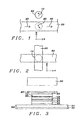
- Fig. 2 there is shown in a schematic overhead view in the xy-plane, the general layout of the MRAM cell of the present invention.
- the MTJ element (10) of substantially circular or low aspect ratio ( ⁇ 2) elliptical cross section, is situated at a junction between a write word line (20), which is above the cell and runs in the y-direction, and a bit line (30), which is below the cell and runs in a direction perpendicular to the write word line (the x-direction).
- the combination of the MTJ element and the write word and bit lines which access and switch the cell form an MTJ MRAM cell.
- a soft magnetic layer is formed on the bottom surface of the bit line and, therefore, cannot be seen in this overhead view.
- the free layer within the cell is proximal to the bit line.
- FIG. 3 there is shown a schematic vertical cross-sectional view (in the xz-plane) of the configuration of Fig. 2.
- the xy-plane will also be referred to as the horizontal plane.
- the MTJ cell (10) of circular or low aspect ratio elliptical cross-section in the xy-plane, is formed between orthogonal write word (20) and bit (30) lines, both of which extend horizontally in the xy-plane but are separated vertically in the z-direction, in accord with the method of the present invention.
- the write word line (20) comes out of the plane of the figure, in the y-direction indicated in Fig. 1.
- the bit line is a composite layer which includes a thin adjacent soft (low coercivity) magnetic layer (32) of high permeability, the SAL, and a conducting layer portion (34), which carries the substantial portion of the bit line current.
- the bit line may be formed in a trench in a dielectric layer over a silicon substrate, but it may also be formed on other substrates. These details are not shown and are not necessary to explain the preferred embodiment.
- the conducting portion (34) of the bit line is formed of a non-magnetic high conductivity material, such as Cu, Au, Al, Ag, CuAg, Ta, Cr, NiCr, NiFeCr, Ru, Rh and their multi-layers and alloys.
- the conducting portion separates the SAL from the free layer of the cell and must be as thin as possible, less than 1000 angstroms, for optimal coupling between the SAL and the free layer.
- the width of the bit line should be greater than the lateral dimension of the cell.
- the SAL is formed of soft magnetic material (low coercivity) such as alloys of Co, Ni and Fe and has a thickness between approximately 50 and 500 angstroms, which should be larger than the thickness of the free layer.
- a seed layer (40) is formed on the bit line and promotes the high quality formation of subsequently formed layers of the cell.
- the seed layer can be a layer of NiCr or NiFe formed to a thickness between approximately 25 and 100 angstroms.
- a single pinned layer or, as in this embodiment, synthetic ferrimagnetic pinned layer (50) is formed on the seed layer.
- the synthetic layer includes an antiferromagnetic pinning layer (52), a first ferromagnetic layer (54), a coupling layer (56) and a second ferromagnetic layer (58).
- the antiferromagnetic layer pins the magnetization of the first ferromagnetic layer unidirectionally through a magnetic annealing process and the second ferromagnetic layer is magnetized in an antiparallel direction to that of the first layer.
- the first and second ferromagnetic layers are layers of CoFe, CoFeB, CoNiFe or NiFe formed to thicknesses between approximately 10 and 200 angstroms and matched so that the net magnetic moment of the configuration is substantially zero.
- the coupling layer is a layer of Rh, Ru, Cr or Cu of proper thickness to maintain strong antiparallel coupling.
- the antiferromagnetic pinning layer (52) can be a layer of PtMn, NiMn, OsMn, IrMn, NiO or CoNiO of thickness between approximately 40 and 300 angstroms.
- a tunneling barrier layer (60) is formed on the second ferromagnetic layer (56) of the pinned layer.
- This layer is a layer of insulating material such as oxidized Al or an oxidized Al-Hf bilayer or a layer of AIN and is formed to a thickness between approximately 7 to 15 angstroms.
- a ferromagnetic free layer (70) is formed on the barrier layer. At this stage of the cell fabrication, it is important to note that the vertical spacing between the SAL and the free layer should less than 1/5 the lateral dimension of the free layer.
- the free layer can be a single layer of ferromagnetic material, such as a layer of CoFe, CoFeB, CoNiFe or NiFe formed to a thickness between approximately 20 and 200 angstroms, or it can be a multilayer, comprising first and second ferromagnetic layers, magnetized in antiparallel directions and separated by a spacer layer of non magnetic but conducting material such as Rh, Ru, Cr or Cu, which is of the proper thickness to maintain strong antiparallel coupling between the two ferromagnetic layers.
- a capping layer (80) is formed on the free layer.
- the capping layer can be a layer of Ru, or Ta formed to a thickness between approximately 10 and 1000 angstroms, or it can be a layer of Al 2 O 3 , TaO or CrO formed to a thickness between approximately 2 and 8 angstroms.
- the MRAM cell is patterned to produce a uniform horizontal cross-section which is circular or elliptical of low aspect ratio.
- the pattern can be made to produce a slightly elliptical shape.
- crystalline uniaxial magnetic anisotropy can be induced in the free layer of the cell during thermal annealing of the antiferromagnetic pinning layer.
- a layer of insulating material (100) surrounds the cell and separates the upper portion of the cell from the write word line. Such insulation is necessary to isolate the cell from the write word line and for the isolation of individual cells formed within an array.
- the word line is a layer of conducting material less than 100 nm in thickness and may be augmented with a cladding layer (44) of magnetic material formed on its surface away from the cell.
- the preferred embodiment of the present invention is illustrative of the present invention rather than being limiting of the present invention. Revisions and modifications may be made to methods, processes, materials, structures, and dimensions through which is formed an MTJ MRAM cell or an MRAM array of such cells, having a composite bit line with an adjacent soft magnetic layer that magnetostatically couples to the cell free layer to make it thermally stable and easily switchable, while still providing such an MRAM cell or array of such cells, formed in accord with the present invention as defined by the appended claims.
Landscapes
- Engineering & Computer Science (AREA)
- Computer Hardware Design (AREA)
- Mram Or Spin Memory Techniques (AREA)
- Semiconductor Memories (AREA)
- Hall/Mr Elements (AREA)
- Thin Magnetic Films (AREA)
- Magnetic Heads (AREA)
Applications Claiming Priority (2)
| Application Number | Priority Date | Filing Date | Title |
|---|---|---|---|
| US10/872,915 US6979586B2 (en) | 2000-10-06 | 2004-06-21 | Magnetic random access memory array with coupled soft adjacent magnetic layer |
| US872915 | 2004-06-21 |
Publications (3)
| Publication Number | Publication Date |
|---|---|
| EP1610341A2 true EP1610341A2 (de) | 2005-12-28 |
| EP1610341A3 EP1610341A3 (de) | 2006-06-14 |
| EP1610341B1 EP1610341B1 (de) | 2009-09-23 |
Family
ID=34942847
Family Applications (1)
| Application Number | Title | Priority Date | Filing Date |
|---|---|---|---|
| EP05392008A Expired - Lifetime EP1610341B1 (de) | 2004-06-21 | 2005-06-14 | Magnetisches Speicherzellenfeld mit benachbarter gekoppelter weichmagnetischer Schicht |
Country Status (7)
| Country | Link |
|---|---|
| US (2) | US6979586B2 (de) |
| EP (1) | EP1610341B1 (de) |
| JP (1) | JP5068939B2 (de) |
| KR (1) | KR100741303B1 (de) |
| AT (1) | ATE443913T1 (de) |
| DE (1) | DE602005016749D1 (de) |
| TW (1) | TWI291696B (de) |
Families Citing this family (79)
| Publication number | Priority date | Publication date | Assignee | Title |
|---|---|---|---|---|
| US7105372B2 (en) * | 2004-01-20 | 2006-09-12 | Headway Technologies, Inc. | Magnetic tunneling junction film structure with process determined in-plane magnetic anisotropy |
| US7211874B2 (en) * | 2004-04-06 | 2007-05-01 | Headway Technologies, Inc. | Magnetic random access memory array with free layer locking mechanism |
| US7132707B2 (en) * | 2004-08-03 | 2006-11-07 | Headway Technologies, Inc. | Magnetic random access memory array with proximate read and write lines cladded with magnetic material |
| US7576956B2 (en) * | 2004-07-26 | 2009-08-18 | Grandis Inc. | Magnetic tunnel junction having diffusion stop layer |
| US7224601B2 (en) | 2005-08-25 | 2007-05-29 | Grandis Inc. | Oscillating-field assisted spin torque switching of a magnetic tunnel junction memory element |
| US7859034B2 (en) * | 2005-09-20 | 2010-12-28 | Grandis Inc. | Magnetic devices having oxide antiferromagnetic layer next to free ferromagnetic layer |
| US7777261B2 (en) | 2005-09-20 | 2010-08-17 | Grandis Inc. | Magnetic device having stabilized free ferromagnetic layer |
| US7973349B2 (en) | 2005-09-20 | 2011-07-05 | Grandis Inc. | Magnetic device having multilayered free ferromagnetic layer |
| US8582252B2 (en) * | 2005-11-02 | 2013-11-12 | Seagate Technology Llc | Magnetic layer with grain refining agent |
| US7430135B2 (en) * | 2005-12-23 | 2008-09-30 | Grandis Inc. | Current-switched spin-transfer magnetic devices with reduced spin-transfer switching current density |
| JP2007194327A (ja) * | 2006-01-18 | 2007-08-02 | Alps Electric Co Ltd | トンネル型磁気検出素子 |
| US20070246787A1 (en) * | 2006-03-29 | 2007-10-25 | Lien-Chang Wang | On-plug magnetic tunnel junction devices based on spin torque transfer switching |
| EP1863034B1 (de) * | 2006-05-04 | 2011-01-05 | Hitachi, Ltd. | Magnetspeichervorrichtung |
| US7486550B2 (en) * | 2006-06-06 | 2009-02-03 | Micron Technology, Inc. | Semiconductor magnetic memory integrating a magnetic tunneling junction above a floating-gate memory cell |
| US7456029B2 (en) * | 2006-06-28 | 2008-11-25 | Magic Technologies, Inc. | Planar flux concentrator for MRAM devices |
| US7502249B1 (en) | 2006-07-17 | 2009-03-10 | Grandis, Inc. | Method and system for using a pulsed field to assist spin transfer induced switching of magnetic memory elements |
| US7532505B1 (en) | 2006-07-17 | 2009-05-12 | Grandis, Inc. | Method and system for using a pulsed field to assist spin transfer induced switching of magnetic memory elements |
| US7851840B2 (en) * | 2006-09-13 | 2010-12-14 | Grandis Inc. | Devices and circuits based on magnetic tunnel junctions utilizing a multilayer barrier |
| TWI330366B (en) * | 2007-02-07 | 2010-09-11 | Ind Tech Res Inst | Magnetic memory device |
| US7957179B2 (en) | 2007-06-27 | 2011-06-07 | Grandis Inc. | Magnetic shielding in magnetic multilayer structures |
| US7982275B2 (en) * | 2007-08-22 | 2011-07-19 | Grandis Inc. | Magnetic element having low saturation magnetization |
| US8659852B2 (en) | 2008-04-21 | 2014-02-25 | Seagate Technology Llc | Write-once magentic junction memory array |
| US7852663B2 (en) | 2008-05-23 | 2010-12-14 | Seagate Technology Llc | Nonvolatile programmable logic gates and adders |
| US7855911B2 (en) | 2008-05-23 | 2010-12-21 | Seagate Technology Llc | Reconfigurable magnetic logic device using spin torque |
| US8223532B2 (en) | 2008-08-07 | 2012-07-17 | Seagate Technology Llc | Magnetic field assisted STRAM cells |
| US7881098B2 (en) | 2008-08-26 | 2011-02-01 | Seagate Technology Llc | Memory with separate read and write paths |
| US7894248B2 (en) | 2008-09-12 | 2011-02-22 | Grandis Inc. | Programmable and redundant circuitry based on magnetic tunnel junction (MTJ) |
| US7985994B2 (en) | 2008-09-29 | 2011-07-26 | Seagate Technology Llc | Flux-closed STRAM with electronically reflective insulative spacer |
| US7746687B2 (en) | 2008-09-30 | 2010-06-29 | Seagate Technology, Llc | Thermally assisted multi-bit MRAM |
| US8169810B2 (en) | 2008-10-08 | 2012-05-01 | Seagate Technology Llc | Magnetic memory with asymmetric energy barrier |
| US8487390B2 (en) * | 2008-10-08 | 2013-07-16 | Seagate Technology Llc | Memory cell with stress-induced anisotropy |
| US8089132B2 (en) | 2008-10-09 | 2012-01-03 | Seagate Technology Llc | Magnetic memory with phonon glass electron crystal material |
| US8039913B2 (en) | 2008-10-09 | 2011-10-18 | Seagate Technology Llc | Magnetic stack with laminated layer |
| US7880209B2 (en) * | 2008-10-09 | 2011-02-01 | Seagate Technology Llc | MRAM cells including coupled free ferromagnetic layers for stabilization |
| US8045366B2 (en) | 2008-11-05 | 2011-10-25 | Seagate Technology Llc | STRAM with composite free magnetic element |
| US8043732B2 (en) | 2008-11-11 | 2011-10-25 | Seagate Technology Llc | Memory cell with radial barrier |
| KR20100052597A (ko) * | 2008-11-11 | 2010-05-20 | 삼성전자주식회사 | 수직형 반도체 장치 |
| US7826181B2 (en) | 2008-11-12 | 2010-11-02 | Seagate Technology Llc | Magnetic memory with porous non-conductive current confinement layer |
| US8289756B2 (en) | 2008-11-25 | 2012-10-16 | Seagate Technology Llc | Non volatile memory including stabilizing structures |
| US7826259B2 (en) | 2009-01-29 | 2010-11-02 | Seagate Technology Llc | Staggered STRAM cell |
| US9368716B2 (en) | 2009-02-02 | 2016-06-14 | Qualcomm Incorporated | Magnetic tunnel junction (MTJ) storage element and spin transfer torque magnetoresistive random access memory (STT-MRAM) cells having an MTJ |
| US8053255B2 (en) | 2009-03-03 | 2011-11-08 | Seagate Technology Llc | STRAM with compensation element and method of making the same |
| US8363459B2 (en) * | 2009-06-11 | 2013-01-29 | Qualcomm Incorporated | Magnetic tunnel junction device and fabrication |
| US7999338B2 (en) | 2009-07-13 | 2011-08-16 | Seagate Technology Llc | Magnetic stack having reference layers with orthogonal magnetization orientation directions |
| JP5655391B2 (ja) * | 2010-06-23 | 2015-01-21 | ソニー株式会社 | 記憶素子及び記憶装置 |
| US9006704B2 (en) | 2011-02-11 | 2015-04-14 | Headway Technologies, Inc. | Magnetic element with improved out-of-plane anisotropy for spintronic applications |
| US20120241878A1 (en) * | 2011-03-24 | 2012-09-27 | International Business Machines Corporation | Magnetic tunnel junction with iron dusting layer between free layer and tunnel barrier |
| US8592927B2 (en) | 2011-05-04 | 2013-11-26 | Magic Technologies, Inc. | Multilayers having reduced perpendicular demagnetizing field using moment dilution for spintronic applications |
| US9007818B2 (en) | 2012-03-22 | 2015-04-14 | Micron Technology, Inc. | Memory cells, semiconductor device structures, systems including such cells, and methods of fabrication |
| US9054030B2 (en) | 2012-06-19 | 2015-06-09 | Micron Technology, Inc. | Memory cells, semiconductor device structures, memory systems, and methods of fabrication |
| US8923038B2 (en) | 2012-06-19 | 2014-12-30 | Micron Technology, Inc. | Memory cells, semiconductor device structures, memory systems, and methods of fabrication |
| JP2013016820A (ja) * | 2012-08-20 | 2013-01-24 | Hitachi Ltd | トンネル磁気抵抗効果素子、それを用いた磁気メモリセル及びランダムアクセスメモリ |
| US9379315B2 (en) | 2013-03-12 | 2016-06-28 | Micron Technology, Inc. | Memory cells, methods of fabrication, semiconductor device structures, and memory systems |
| US9368714B2 (en) | 2013-07-01 | 2016-06-14 | Micron Technology, Inc. | Memory cells, methods of operation and fabrication, semiconductor device structures, and memory systems |
| US9466787B2 (en) | 2013-07-23 | 2016-10-11 | Micron Technology, Inc. | Memory cells, methods of fabrication, semiconductor device structures, memory systems, and electronic systems |
| US9461242B2 (en) | 2013-09-13 | 2016-10-04 | Micron Technology, Inc. | Magnetic memory cells, methods of fabrication, semiconductor devices, memory systems, and electronic systems |
| US9608197B2 (en) | 2013-09-18 | 2017-03-28 | Micron Technology, Inc. | Memory cells, methods of fabrication, and semiconductor devices |
| US10454024B2 (en) | 2014-02-28 | 2019-10-22 | Micron Technology, Inc. | Memory cells, methods of fabrication, and memory devices |
| US9281466B2 (en) | 2014-04-09 | 2016-03-08 | Micron Technology, Inc. | Memory cells, semiconductor structures, semiconductor devices, and methods of fabrication |
| US9269888B2 (en) | 2014-04-18 | 2016-02-23 | Micron Technology, Inc. | Memory cells, methods of fabrication, and semiconductor devices |
| US9349945B2 (en) | 2014-10-16 | 2016-05-24 | Micron Technology, Inc. | Memory cells, semiconductor devices, and methods of fabrication |
| US9768377B2 (en) | 2014-12-02 | 2017-09-19 | Micron Technology, Inc. | Magnetic cell structures, and methods of fabrication |
| US10439131B2 (en) | 2015-01-15 | 2019-10-08 | Micron Technology, Inc. | Methods of forming semiconductor devices including tunnel barrier materials |
| KR102465539B1 (ko) | 2015-09-18 | 2022-11-11 | 삼성전자주식회사 | 자기 터널 접합 구조체를 포함하는 반도체 소자 및 그의 형성 방법 |
| US9966529B1 (en) | 2017-03-17 | 2018-05-08 | Headway Technologies, Inc. | MgO insertion into free layer for magnetic memory applications |
| US10276784B1 (en) * | 2017-10-30 | 2019-04-30 | Taiwan Semiconductor Manufacturing Company Ltd. | Semiconductor structure and associated operating and fabricating method |
| US10325639B2 (en) | 2017-11-20 | 2019-06-18 | Taiwan Semiconductor Manufacturing Company, Ltd. | Initialization process for magnetic random access memory (MRAM) production |
| US10522745B2 (en) | 2017-12-14 | 2019-12-31 | Taiwan Semiconductor Manufacturing Company, Ltd. | Low resistance MgO capping layer for perpendicularly magnetized magnetic tunnel junctions |
| US10665773B2 (en) | 2018-01-26 | 2020-05-26 | Taiwan Semiconductor Manufacturing Company, Ltd. | Nitride capping layer for spin torque transfer (STT)-magnetoresistive random access memory (MRAM) |
| CN109244233B (zh) * | 2018-07-26 | 2021-02-19 | 西安交通大学 | 基于人工反铁磁固定层的磁性隧道结器件及随机存储装置 |
| US10522746B1 (en) | 2018-08-07 | 2019-12-31 | Taiwan Semiconductor Manufacturing Company, Ltd. | Dual magnetic tunnel junction devices for magnetic random access memory (MRAM) |
| US10797225B2 (en) | 2018-09-18 | 2020-10-06 | Taiwan Semiconductor Manufacturing Company, Ltd. | Dual magnetic tunnel junction (DMTJ) stack design |
| US10950782B2 (en) | 2019-02-14 | 2021-03-16 | Headway Technologies, Inc. | Nitride diffusion barrier structure for spintronic applications |
| US11264566B2 (en) | 2019-06-21 | 2022-03-01 | Headway Technologies, Inc. | Magnetic element with perpendicular magnetic anisotropy (PMA) and improved coercivity field (Hc)/switching current ratio |
| US11264560B2 (en) | 2019-06-21 | 2022-03-01 | Headway Technologies, Inc. | Minimal thickness, low switching voltage magnetic free layers using an oxidation control layer and magnetic moment tuning layer for spintronic applications |
| CN115691596A (zh) * | 2021-07-27 | 2023-02-03 | 浙江驰拓科技有限公司 | 磁性存储单元及磁性存储器 |
| CN113744777B (zh) * | 2021-09-08 | 2024-01-02 | 北京航空航天大学 | 磁性随机存储器的存储单元及数据多态存储控制方法 |
| US11823724B2 (en) | 2021-10-26 | 2023-11-21 | International Business Machines Corporation | Magneto-electric low power analogue magnetic tunnel junction memory |
| KR20230093928A (ko) * | 2021-12-20 | 2023-06-27 | 에스케이하이닉스 주식회사 | 전자 장치 |
Citations (6)
| Publication number | Priority date | Publication date | Assignee | Title |
|---|---|---|---|---|
| US5650958A (en) | 1996-03-18 | 1997-07-22 | International Business Machines Corporation | Magnetic tunnel junctions with controlled magnetic response |
| US5966323A (en) | 1997-12-18 | 1999-10-12 | Motorola, Inc. | Low switching field magnetoresistive tunneling junction for high density arrays |
| US6166948A (en) | 1999-09-03 | 2000-12-26 | International Business Machines Corporation | Magnetic memory array with magnetic tunnel junction memory cells having flux-closed free layers |
| US6211090B1 (en) | 2000-03-21 | 2001-04-03 | Motorola, Inc. | Method of fabricating flux concentrating layer for use with magnetoresistive random access memories |
| US6531723B1 (en) | 2001-10-16 | 2003-03-11 | Motorola, Inc. | Magnetoresistance random access memory for improved scalability |
| US6611405B1 (en) | 1999-09-16 | 2003-08-26 | Kabushiki Kaisha Toshiba | Magnetoresistive element and magnetic memory device |
Family Cites Families (7)
| Publication number | Priority date | Publication date | Assignee | Title |
|---|---|---|---|---|
| US5969978A (en) * | 1998-09-30 | 1999-10-19 | The United States Of America As Represented By The Secretary Of The Navy | Read/write memory architecture employing closed ring elements |
| US6005800A (en) * | 1998-11-23 | 1999-12-21 | International Business Machines Corporation | Magnetic memory array with paired asymmetric memory cells for improved write margin |
| US6872993B1 (en) * | 1999-05-25 | 2005-03-29 | Micron Technology, Inc. | Thin film memory device having local and external magnetic shielding |
| US6936903B2 (en) * | 2001-09-25 | 2005-08-30 | Hewlett-Packard Development Company, L.P. | Magnetic memory cell having a soft reference layer |
| US6740947B1 (en) * | 2002-11-13 | 2004-05-25 | Hewlett-Packard Development Company, L.P. | MRAM with asymmetric cladded conductor |
| JP2004273969A (ja) * | 2003-03-12 | 2004-09-30 | Sony Corp | 磁気記憶装置の製造方法 |
| US7211874B2 (en) | 2004-04-06 | 2007-05-01 | Headway Technologies, Inc. | Magnetic random access memory array with free layer locking mechanism |
-
2004
- 2004-06-21 US US10/872,915 patent/US6979586B2/en not_active Expired - Lifetime
-
2005
- 2005-06-14 AT AT05392008T patent/ATE443913T1/de not_active IP Right Cessation
- 2005-06-14 DE DE602005016749T patent/DE602005016749D1/de not_active Expired - Lifetime
- 2005-06-14 EP EP05392008A patent/EP1610341B1/de not_active Expired - Lifetime
- 2005-06-21 TW TW094120561A patent/TWI291696B/zh not_active IP Right Cessation
- 2005-06-21 JP JP2005180553A patent/JP5068939B2/ja not_active Expired - Fee Related
- 2005-06-21 KR KR1020050053650A patent/KR100741303B1/ko not_active Expired - Lifetime
- 2005-08-25 US US11/210,637 patent/US7335961B2/en not_active Expired - Fee Related
Patent Citations (6)
| Publication number | Priority date | Publication date | Assignee | Title |
|---|---|---|---|---|
| US5650958A (en) | 1996-03-18 | 1997-07-22 | International Business Machines Corporation | Magnetic tunnel junctions with controlled magnetic response |
| US5966323A (en) | 1997-12-18 | 1999-10-12 | Motorola, Inc. | Low switching field magnetoresistive tunneling junction for high density arrays |
| US6166948A (en) | 1999-09-03 | 2000-12-26 | International Business Machines Corporation | Magnetic memory array with magnetic tunnel junction memory cells having flux-closed free layers |
| US6611405B1 (en) | 1999-09-16 | 2003-08-26 | Kabushiki Kaisha Toshiba | Magnetoresistive element and magnetic memory device |
| US6211090B1 (en) | 2000-03-21 | 2001-04-03 | Motorola, Inc. | Method of fabricating flux concentrating layer for use with magnetoresistive random access memories |
| US6531723B1 (en) | 2001-10-16 | 2003-03-11 | Motorola, Inc. | Magnetoresistance random access memory for improved scalability |
Also Published As
| Publication number | Publication date |
|---|---|
| JP2006013498A (ja) | 2006-01-12 |
| EP1610341A3 (de) | 2006-06-14 |
| US20050280960A1 (en) | 2005-12-22 |
| JP5068939B2 (ja) | 2012-11-07 |
| ATE443913T1 (de) | 2009-10-15 |
| TWI291696B (en) | 2007-12-21 |
| KR20060046496A (ko) | 2006-05-17 |
| KR100741303B1 (ko) | 2007-07-23 |
| TW200617953A (en) | 2006-06-01 |
| DE602005016749D1 (de) | 2009-11-05 |
| US7335961B2 (en) | 2008-02-26 |
| US20040233760A1 (en) | 2004-11-25 |
| US6979586B2 (en) | 2005-12-27 |
| EP1610341B1 (de) | 2009-09-23 |
Similar Documents
| Publication | Publication Date | Title |
|---|---|---|
| US7335961B2 (en) | Magnetic random access memory array with coupled soft adjacent magnetic layer | |
| US7105372B2 (en) | Magnetic tunneling junction film structure with process determined in-plane magnetic anisotropy | |
| US7443707B2 (en) | Magnetic random access memory array with free layer locking mechanism and method of its use | |
| JP4815051B2 (ja) | 低切替磁界磁性トンネル接合 | |
| US7394122B2 (en) | Magnetic random access memory array with thin conduction electrical read and write lines | |
| US7072208B2 (en) | Vortex magnetic random access memory | |
| CN103035280B (zh) | 磁随机存取存储器单元、用于对其进行读取和写入的方法 | |
| JP4226295B2 (ja) | 磁気的に軟らかい基準層を有する磁気抵抗素子 | |
| US7132707B2 (en) | Magnetic random access memory array with proximate read and write lines cladded with magnetic material | |
| JP2005522044A (ja) | 高密度mram用途用の合成フェリ磁性体センス層 | |
| US9679624B2 (en) | Magnetic random access memory (MRAM) cell with low power consumption | |
| JP2003188359A (ja) | 磁気的に軟らかい合成フェリ磁性体基準層を含む磁気抵抗素子 |
Legal Events
| Date | Code | Title | Description |
|---|---|---|---|
| PUAI | Public reference made under article 153(3) epc to a published international application that has entered the european phase |
Free format text: ORIGINAL CODE: 0009012 |
|
| AK | Designated contracting states |
Kind code of ref document: A2 Designated state(s): AT BE BG CH CY CZ DE DK EE ES FI FR GB GR HU IE IS IT LI LT LU MC NL PL PT RO SE SI SK TR |
|
| AX | Request for extension of the european patent |
Extension state: AL BA HR LV MK YU |
|
| PUAL | Search report despatched |
Free format text: ORIGINAL CODE: 0009013 |
|
| AK | Designated contracting states |
Kind code of ref document: A3 Designated state(s): AT BE BG CH CY CZ DE DK EE ES FI FR GB GR HU IE IS IT LI LT LU MC NL PL PT RO SE SI SK TR |
|
| AX | Request for extension of the european patent |
Extension state: AL BA HR LV MK YU |
|
| 17P | Request for examination filed |
Effective date: 20061213 |
|
| 17Q | First examination report despatched |
Effective date: 20070117 |
|
| AKX | Designation fees paid |
Designated state(s): AT BE BG CH CY CZ DE DK EE ES FI FR GB GR HU IE IS IT LI LT LU MC NL PL PT RO SE SI SK TR |
|
| GRAP | Despatch of communication of intention to grant a patent |
Free format text: ORIGINAL CODE: EPIDOSNIGR1 |
|
| GRAS | Grant fee paid |
Free format text: ORIGINAL CODE: EPIDOSNIGR3 |
|
| GRAA | (expected) grant |
Free format text: ORIGINAL CODE: 0009210 |
|
| AK | Designated contracting states |
Kind code of ref document: B1 Designated state(s): AT BE BG CH CY CZ DE DK EE ES FI FR GB GR HU IE IS IT LI LT LU MC NL PL PT RO SE SI SK TR |
|
| REG | Reference to a national code |
Ref country code: GB Ref legal event code: FG4D |
|
| REG | Reference to a national code |
Ref country code: CH Ref legal event code: EP |
|
| REG | Reference to a national code |
Ref country code: IE Ref legal event code: FG4D |
|
| REF | Corresponds to: |
Ref document number: 602005016749 Country of ref document: DE Date of ref document: 20091105 Kind code of ref document: P |
|
| PG25 | Lapsed in a contracting state [announced via postgrant information from national office to epo] |
Ref country code: FI Free format text: LAPSE BECAUSE OF FAILURE TO SUBMIT A TRANSLATION OF THE DESCRIPTION OR TO PAY THE FEE WITHIN THE PRESCRIBED TIME-LIMIT Effective date: 20090923 Ref country code: LT Free format text: LAPSE BECAUSE OF FAILURE TO SUBMIT A TRANSLATION OF THE DESCRIPTION OR TO PAY THE FEE WITHIN THE PRESCRIBED TIME-LIMIT Effective date: 20090923 Ref country code: SE Free format text: LAPSE BECAUSE OF FAILURE TO SUBMIT A TRANSLATION OF THE DESCRIPTION OR TO PAY THE FEE WITHIN THE PRESCRIBED TIME-LIMIT Effective date: 20090923 |
|
| LTIE | Lt: invalidation of european patent or patent extension |
Effective date: 20090923 |
|
| PG25 | Lapsed in a contracting state [announced via postgrant information from national office to epo] |
Ref country code: PL Free format text: LAPSE BECAUSE OF FAILURE TO SUBMIT A TRANSLATION OF THE DESCRIPTION OR TO PAY THE FEE WITHIN THE PRESCRIBED TIME-LIMIT Effective date: 20090923 Ref country code: SI Free format text: LAPSE BECAUSE OF FAILURE TO SUBMIT A TRANSLATION OF THE DESCRIPTION OR TO PAY THE FEE WITHIN THE PRESCRIBED TIME-LIMIT Effective date: 20090923 |
|
| NLV1 | Nl: lapsed or annulled due to failure to fulfill the requirements of art. 29p and 29m of the patents act | ||
| PG25 | Lapsed in a contracting state [announced via postgrant information from national office to epo] |
Ref country code: CY Free format text: LAPSE BECAUSE OF FAILURE TO SUBMIT A TRANSLATION OF THE DESCRIPTION OR TO PAY THE FEE WITHIN THE PRESCRIBED TIME-LIMIT Effective date: 20090923 |
|
| PG25 | Lapsed in a contracting state [announced via postgrant information from national office to epo] |
Ref country code: PT Free format text: LAPSE BECAUSE OF FAILURE TO SUBMIT A TRANSLATION OF THE DESCRIPTION OR TO PAY THE FEE WITHIN THE PRESCRIBED TIME-LIMIT Effective date: 20100125 Ref country code: CZ Free format text: LAPSE BECAUSE OF FAILURE TO SUBMIT A TRANSLATION OF THE DESCRIPTION OR TO PAY THE FEE WITHIN THE PRESCRIBED TIME-LIMIT Effective date: 20090923 Ref country code: RO Free format text: LAPSE BECAUSE OF FAILURE TO SUBMIT A TRANSLATION OF THE DESCRIPTION OR TO PAY THE FEE WITHIN THE PRESCRIBED TIME-LIMIT Effective date: 20090923 Ref country code: IS Free format text: LAPSE BECAUSE OF FAILURE TO SUBMIT A TRANSLATION OF THE DESCRIPTION OR TO PAY THE FEE WITHIN THE PRESCRIBED TIME-LIMIT Effective date: 20100123 Ref country code: ES Free format text: LAPSE BECAUSE OF FAILURE TO SUBMIT A TRANSLATION OF THE DESCRIPTION OR TO PAY THE FEE WITHIN THE PRESCRIBED TIME-LIMIT Effective date: 20100103 Ref country code: EE Free format text: LAPSE BECAUSE OF FAILURE TO SUBMIT A TRANSLATION OF THE DESCRIPTION OR TO PAY THE FEE WITHIN THE PRESCRIBED TIME-LIMIT Effective date: 20090923 |
|
| PG25 | Lapsed in a contracting state [announced via postgrant information from national office to epo] |
Ref country code: SK Free format text: LAPSE BECAUSE OF FAILURE TO SUBMIT A TRANSLATION OF THE DESCRIPTION OR TO PAY THE FEE WITHIN THE PRESCRIBED TIME-LIMIT Effective date: 20090923 |
|
| PG25 | Lapsed in a contracting state [announced via postgrant information from national office to epo] |
Ref country code: BE Free format text: LAPSE BECAUSE OF FAILURE TO SUBMIT A TRANSLATION OF THE DESCRIPTION OR TO PAY THE FEE WITHIN THE PRESCRIBED TIME-LIMIT Effective date: 20090923 Ref country code: AT Free format text: LAPSE BECAUSE OF FAILURE TO SUBMIT A TRANSLATION OF THE DESCRIPTION OR TO PAY THE FEE WITHIN THE PRESCRIBED TIME-LIMIT Effective date: 20090923 |
|
| PG25 | Lapsed in a contracting state [announced via postgrant information from national office to epo] |
Ref country code: DK Free format text: LAPSE BECAUSE OF FAILURE TO SUBMIT A TRANSLATION OF THE DESCRIPTION OR TO PAY THE FEE WITHIN THE PRESCRIBED TIME-LIMIT Effective date: 20090923 Ref country code: NL Free format text: LAPSE BECAUSE OF FAILURE TO SUBMIT A TRANSLATION OF THE DESCRIPTION OR TO PAY THE FEE WITHIN THE PRESCRIBED TIME-LIMIT Effective date: 20090923 |
|
| PLBE | No opposition filed within time limit |
Free format text: ORIGINAL CODE: 0009261 |
|
| STAA | Information on the status of an ep patent application or granted ep patent |
Free format text: STATUS: NO OPPOSITION FILED WITHIN TIME LIMIT |
|
| 26N | No opposition filed |
Effective date: 20100624 |
|
| PG25 | Lapsed in a contracting state [announced via postgrant information from national office to epo] |
Ref country code: GR Free format text: LAPSE BECAUSE OF FAILURE TO SUBMIT A TRANSLATION OF THE DESCRIPTION OR TO PAY THE FEE WITHIN THE PRESCRIBED TIME-LIMIT Effective date: 20091224 |
|
| PG25 | Lapsed in a contracting state [announced via postgrant information from national office to epo] |
Ref country code: MC Free format text: LAPSE BECAUSE OF NON-PAYMENT OF DUE FEES Effective date: 20100630 |
|
| REG | Reference to a national code |
Ref country code: CH Ref legal event code: PL |
|
| GBPC | Gb: european patent ceased through non-payment of renewal fee |
Effective date: 20100614 |
|
| PG25 | Lapsed in a contracting state [announced via postgrant information from national office to epo] |
Ref country code: IT Free format text: LAPSE BECAUSE OF FAILURE TO SUBMIT A TRANSLATION OF THE DESCRIPTION OR TO PAY THE FEE WITHIN THE PRESCRIBED TIME-LIMIT Effective date: 20090923 |
|
| PG25 | Lapsed in a contracting state [announced via postgrant information from national office to epo] |
Ref country code: IE Free format text: LAPSE BECAUSE OF NON-PAYMENT OF DUE FEES Effective date: 20100614 Ref country code: LI Free format text: LAPSE BECAUSE OF NON-PAYMENT OF DUE FEES Effective date: 20100630 Ref country code: CH Free format text: LAPSE BECAUSE OF NON-PAYMENT OF DUE FEES Effective date: 20100630 |
|
| PG25 | Lapsed in a contracting state [announced via postgrant information from national office to epo] |
Ref country code: GB Free format text: LAPSE BECAUSE OF NON-PAYMENT OF DUE FEES Effective date: 20100614 |
|
| PG25 | Lapsed in a contracting state [announced via postgrant information from national office to epo] |
Ref country code: LU Free format text: LAPSE BECAUSE OF NON-PAYMENT OF DUE FEES Effective date: 20100614 Ref country code: BG Free format text: LAPSE BECAUSE OF FAILURE TO SUBMIT A TRANSLATION OF THE DESCRIPTION OR TO PAY THE FEE WITHIN THE PRESCRIBED TIME-LIMIT Effective date: 20090923 Ref country code: HU Free format text: LAPSE BECAUSE OF FAILURE TO SUBMIT A TRANSLATION OF THE DESCRIPTION OR TO PAY THE FEE WITHIN THE PRESCRIBED TIME-LIMIT Effective date: 20100324 |
|
| PG25 | Lapsed in a contracting state [announced via postgrant information from national office to epo] |
Ref country code: TR Free format text: LAPSE BECAUSE OF FAILURE TO SUBMIT A TRANSLATION OF THE DESCRIPTION OR TO PAY THE FEE WITHIN THE PRESCRIBED TIME-LIMIT Effective date: 20090923 |
|
| PGFP | Annual fee paid to national office [announced via postgrant information from national office to epo] |
Ref country code: DE Payment date: 20130627 Year of fee payment: 9 |
|
| PGFP | Annual fee paid to national office [announced via postgrant information from national office to epo] |
Ref country code: FR Payment date: 20130712 Year of fee payment: 9 |
|
| REG | Reference to a national code |
Ref country code: DE Ref legal event code: R119 Ref document number: 602005016749 Country of ref document: DE |
|
| REG | Reference to a national code |
Ref country code: FR Ref legal event code: ST Effective date: 20150227 |
|
| REG | Reference to a national code |
Ref country code: DE Ref legal event code: R119 Ref document number: 602005016749 Country of ref document: DE Effective date: 20150101 |
|
| PG25 | Lapsed in a contracting state [announced via postgrant information from national office to epo] |
Ref country code: DE Free format text: LAPSE BECAUSE OF NON-PAYMENT OF DUE FEES Effective date: 20150101 |
|
| PG25 | Lapsed in a contracting state [announced via postgrant information from national office to epo] |
Ref country code: FR Free format text: LAPSE BECAUSE OF NON-PAYMENT OF DUE FEES Effective date: 20140630 |