EP1612298A2 - Elektroplattierungskopf und Verfahren zu dessen Gebrauch - Google Patents
Elektroplattierungskopf und Verfahren zu dessen Gebrauch Download PDFInfo
- Publication number
- EP1612298A2 EP1612298A2 EP05253928A EP05253928A EP1612298A2 EP 1612298 A2 EP1612298 A2 EP 1612298A2 EP 05253928 A EP05253928 A EP 05253928A EP 05253928 A EP05253928 A EP 05253928A EP 1612298 A2 EP1612298 A2 EP 1612298A2
- Authority
- EP
- European Patent Office
- Prior art keywords
- electroplating
- wafer
- anode
- head
- recited
- Prior art date
- Legal status (The legal status is an assumption and is not a legal conclusion. Google has not performed a legal analysis and makes no representation as to the accuracy of the status listed.)
- Withdrawn
Links
Images




Classifications
-
- C—CHEMISTRY; METALLURGY
- C25—ELECTROLYTIC OR ELECTROPHORETIC PROCESSES; APPARATUS THEREFOR
- C25D—PROCESSES FOR THE ELECTROLYTIC OR ELECTROPHORETIC PRODUCTION OF COATINGS; ELECTROFORMING; APPARATUS THEREFOR
- C25D17/00—Constructional parts, or assemblies thereof, of cells for electrolytic coating
- C25D17/10—Electrodes, e.g. composition, counter electrode
-
- C—CHEMISTRY; METALLURGY
- C25—ELECTROLYTIC OR ELECTROPHORETIC PROCESSES; APPARATUS THEREFOR
- C25D—PROCESSES FOR THE ELECTROLYTIC OR ELECTROPHORETIC PRODUCTION OF COATINGS; ELECTROFORMING; APPARATUS THEREFOR
- C25D5/00—Electroplating characterised by the process; Pretreatment or after-treatment of workpieces
- C25D5/02—Electroplating of selected surface areas
- C25D5/026—Electroplating of selected surface areas using locally applied jets of electrolyte
-
- C—CHEMISTRY; METALLURGY
- C25—ELECTROLYTIC OR ELECTROPHORETIC PROCESSES; APPARATUS THEREFOR
- C25D—PROCESSES FOR THE ELECTROLYTIC OR ELECTROPHORETIC PRODUCTION OF COATINGS; ELECTROFORMING; APPARATUS THEREFOR
- C25D17/00—Constructional parts, or assemblies thereof, of cells for electrolytic coating
- C25D17/10—Electrodes, e.g. composition, counter electrode
- C25D17/14—Electrodes, e.g. composition, counter electrode for pad-plating
-
- C—CHEMISTRY; METALLURGY
- C25—ELECTROLYTIC OR ELECTROPHORETIC PROCESSES; APPARATUS THEREFOR
- C25D—PROCESSES FOR THE ELECTROLYTIC OR ELECTROPHORETIC PRODUCTION OF COATINGS; ELECTROFORMING; APPARATUS THEREFOR
- C25D5/00—Electroplating characterised by the process; Pretreatment or after-treatment of workpieces
- C25D5/02—Electroplating of selected surface areas
-
- C—CHEMISTRY; METALLURGY
- C25—ELECTROLYTIC OR ELECTROPHORETIC PROCESSES; APPARATUS THEREFOR
- C25D—PROCESSES FOR THE ELECTROLYTIC OR ELECTROPHORETIC PRODUCTION OF COATINGS; ELECTROFORMING; APPARATUS THEREFOR
- C25D5/00—Electroplating characterised by the process; Pretreatment or after-treatment of workpieces
- C25D5/04—Electroplating with moving electrodes
- C25D5/06—Brush or pad plating
Definitions
- the semiconductor wafers include integrated circuit devices in the form of multi-level structures defined on a silicon substrate. At a substrate level, transistor devices with diffusion regions are formed. In subsequent levels, interconnect metallization lines are patterned and electrically connected to the transistor devices to define a desired integrated circuit device. Also, patterned conductive layers are insulated from other conductive layers by dielectric materials.
- the series of manufacturing operations for defining features on the semiconductor wafers can include an electroplating process for adding material to the surface of the semiconductor wafer.
- electroplating is performed in a complete wafer electroplating processor with the entire wafer submerged in an electrolyte.
- the wafer is maintained at a negative potential with respect to a positively charged anode plate, wherein the anode plate is substantially equal in size to the wafer.
- the anode plate is also submerged in the electrolyte and maintained in a position proximate to and parallel with the wafer.
- the wafer acts as a cathode.
- the wafer is required to be electrically connected to a number of electrodes.
- the number of electrodes are required to be uniformly distributed around a perimeter of the wafer and have substantially matched contact resistances in order to achieve a uniform current distribution across the wafer.
- a non-uniform current distribution across the wafer can result in a non-uniform plating thickness across the wafer.
- an electroplating head in one embodiment, includes a chamber having a fluid entrance and a fluid exit.
- the chamber is configured to contain a flow of electroplating solution from the fluid entrance to the fluid exit.
- the electroplating head also includes an anode disposed within the chamber. The anode is configured to be electrically connected to a power supply.
- the electroplating head further includes a porous resistive material disposed at the fluid exit such that the flow of electroplating solution is required to traverse through the porous resistive material.
- an apparatus for electroplating a semiconductor wafer includes a wafer support configured to hold a wafer.
- the apparatus also includes an electroplating head configured to be disposed over an upper surface of the wafer to be held by the wafer support.
- the electroplating head is configured to have a processing area defined to be substantially parallel with and proximate to an upper surface of the wafer.
- the processing area is defined by a long dimension that is at least equal to a diameter of the wafer and a short dimension that is less than the diameter of the wafer.
- the processing area is further defined as an exterior surface area of a porous resistive material.
- the apparatus further includes a first electrode disposed at a first location proximate to a first peripheral half of the wafer support.
- the first electrode is movably configured to electrically contact the wafer to be held by the wafer support.
- the apparatus includes a second electrode disposed at a second location proximate to a second peripheral half of the wafer support that is exclusive of the first peripheral half of the wafer support.
- the second electrode is movably configured to electrically contact the wafer to be held by the wafer support.
- the electroplating head and the wafer support are configured to move with respect to one another in a direction extending between the first electrode and the second electrode, such that the electroplating head can traverse over an entirety of the upper surface of the wafer when the wafer is held by the wafer support.
- a method for operating an electroplating head includes an operation for disposing an electroplating head over and proximate to an upper surface of a wafer.
- the method also includes an operation for transferring cations from an anode to an electroplating solution within the electroplating head.
- the electroplating solution is flowed through a porous resistive material to exit the electroplating head and be disposed on the upper surface of the wafer.
- the method further includes an operation for establishing an electric current between the anode and the upper surface of the wafer through the electroplating solution.
- the electric current is uniformly distributed by the porous resistive material present between the anode and the upper surface of the wafer. Also, the electric current causes the cations to be attracted to the upper surface of the wafer.
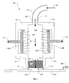
- FIG. 1 is an illustration showing an electroplating head 100 disposed over a wafer 307, in accordance with one embodiment of the present invention.
- the electroplating head 100 includes a main chamber 105 formed within surrounding walls 101. It should be appreciated that the surrounding walls 101 can be defined in either an integral manner or as a combination of appropriately fastened and sealed components.
- the main chamber 105 includes a fluid entrance 111 and a fluid exit 112.
- a fluid supply 113 is attached to the fluid entrance 111 to supply electroplating solution to the main chamber 105.
- the main chamber 105 is configured to contain a flow of electroplating solution from the fluid entrance 111 to the fluid exit 112, as indicated by arrows 301.
- the electroplating head 100 also includes a first anode 115A and a second anode 115B disposed within anode chambers 105A and 105B, respectively.
- Each of the anodes 115A/115B is configured to be electrically connected to a power supply as indicated by a positive polarity 117.
- a shape and an orientation of each anode 115A/115B within its respective anode chamber 105A/105B can be defined in a number of different ways.
- anodes 115A/115B and associated anode chambers 105A/105B can be configured in various ways within the electroplating head 100, it is desirable to establish the anodes 115A/115B and associated anode chambers 105A/105B in a manner that will provide a substantially uniform distribution of cations throughout the electroplating solution within the main chamber 105.
- the anodes 115A/115B are disposed with their respective anode chambers 105A/105B in a vertical orientation.
- the vertical orientation of the anodes 115A/115B enables natural circulation of an electroplating solution present within the respective anode chambers 105A/105B.
- the natural circulation can be induced by gravity acting upon particulate materials released from the anodes 115A/115B during the electroplating process.
- the vertical orientation of the anodes 115A/115B corresponds to a perpendicular orientation of the anodes 115A/115B with respect to the wafer 307.
- anode polarization can occur when solubility limits of dissolving ions cause precipitation of salts at the anode surface.
- the precipitated salts cause the anode to be insulated from the surrounding electroplating solution.
- the anode polarization effect is generally associated with exceeding a critical current flux during the electroplating process.
- decreasing areas of uninsulated anode become responsible for providing an increased current flux.
- a precipitate cascade results in a shut-down of reactions at the anode.
- the vertical orientation of anodes within the anode chambers provides for mass transfer within anode chambers via natural convection, thus resulting in circulation of the electroplating solution within the anode chambers.
- the circulation of electroplating solution within the anode chambers prevents adhesion of precipitated salts to surfaces of the anode.
- the vertical orientation of each anode within its respective anode chamber avoids electroplating head design complexity, electroplating process complexity, and increased expense associated with having to mechanically circulate electroplating solution in order to reduce deposition of precipitated salts on the anode.
- the vertical orientation of each anode allows for an increase in a maximum allowable current flux.
- electroplating head 100 shows the electroplating head 100 as including two anodes 115A/115B and associated anode chambers 105A/105B, it should be appreciated that in other embodiments the electroplating head 100 can include one or more anodes and associated anode chambers. Use of more anodes serves to increase current flux to the cathode, i.e., the wafer 307.
- each of the anode chambers 105A and 105B is configured to be filled with electroplating solution.
- the electroplating solution within each of the anode chambers 105A and 105B is separated from the main chamber 105 by a membrane 109A and 109B, respectively.
- the electroplating solution within the anode chambers 105A/105B is referred to as analyte.
- the electroplating solution within the main chamber 105 is referred to as catalyte.
- the analyte present within the anode chambers 105A/105B can be defined to have a chemistry that is either equivalent to or different from the chemistry of the catalyte present within the main chamber 105. Since the anode chambers 105A/105B are filled with analyte, there is essentially no air present in the anode chambers 105A/105B. Thus, the analyte within the anode chambers 105A/105B is rendered incompressible, thereby reducing a possibility that analyte will be transferred and mixed with catalyte present in the main chamber 105. Also, the incompressibility of the anode chambers 105A/105B allows a pressure within the main chamber 105 to be increased without causing distortion of the membranes 109A/109B.
- each membrane 109A and 109B is defined to allow cations to pass from the anode chambers 105A and 105B, respectively, to the main chamber 105, as indicated by arrows 303.
- the membranes 109A/109B are configured to prevent passage into the main chamber 105 of materials, e.g., particles and gases, from the anode chambers 105A/105B that could be detrimental to the electroplating process.
- the membrane 109A/109B is defined by a fluorocarbon material.
- the membrane 109A/109B is defined to have a pore size, i.e., average pore diameter, within a range extending from about 0.2 micrometer to about 0.05 micrometer.
- the pore size of the membranes 109A/109B is sufficient to allow passage of cations from the anode chamber 105A/105B to the main chamber 105, without allowing passage from the anode chamber 105A/105B to the main chamber 105 of particulate materials generated by anodic reactions. Therefore, using the membranes 109A/109B to separate the analyte from the catalyte, as provided by the present invention, avoids problems associated with unwanted foreign particle transport from the anode to the wafer during the electroplating process.
- key organic additives are included within the catalyte to enhance the electroplating process performance at the cathode, i.e., wafer.
- these key organic additives arc vulnerable to being consumed by the anode, thus reducing the additives available for the electroplating process at the cathode without replenishment of these additives. Consumption of the key organic additives by the anode is particularly problematic in the presence of copper (Cu) metal.
- the membranes 109A/109B of the present invention serve to prevent these key organic additives present in the catalyte of the main chamber 105 from mixing with the analyte or being exposed to the copper electrodes in the anode chambers 105A/105B.
- the membranes 109A/109B serve to prevent these key organic additives present in the catalyte of the main chamber 105 from mixing with the analyte or being exposed to the copper electrodes in the anode chambers 105A/105B.
- the membranes 109A/109B the key organic additives are not exposed to the anodes 115A/115B.
- a concentration of the key organic additives in the catalyte can be more closely controlled.
- the electroplating head 100 also includes a porous resistive material 119 disposed at the fluid exit 112.
- the catalyte within the main chamber 105 is required to traverse through the porous resistive material 119 in order to exit the electroplating head 100 at a processing area 201, as indicated by arrow 301.
- the processing area 201 is defined by a lower surface of the porous resistive material 119.
- the processing area 201 of the electroplating head 100 is positioned over, proximate to, and parallel with an upper surface of the wafer 307 to be processed.
- the meniscus 305 essentially represents an electroplating reaction chamber defined by the processing area 201 of the electroplating head 100 and a distance between the processing area 201 and the wafer 307.
- meniscus confinement surfaces 311 can be incorporated to assist in maintaining the meniscus within the region directly below the processing area 201.
- the meniscus confinement surfaces 311 represent one or more surfaces that extend below the processing area 201 toward the wafer 307 at a periphery of the processing area 201. It should be understood, however, that the meniscus confinement surfaces 311 are not required for successful operation of the electroplating head 100.
- a voltage potential is maintained between the anodes 115A/115B and the wafer 307, as indicated by a negative polarity 309.
- an electric current is established between the anodes 115A/115B and the wafer 307 via the electroplating solution (catalyte and analyte).
- the electric current causes metal ions (cations) produced at the anode to diffuse through the membranes 109A/109B to be carried by the catalyte through the porous resistive material 119 to the wafer 307 where plating occurs.
- the porous resistive material 119 serves to uniformly distribute the electric current established between the anodes 115A/115B and the wafer 307. Establishment of a more uniformly distributed electric current across the wafer 307 surface results in a more uniform material deposition.
- the porous resistive material 119 serves to provide a more uniform material deposition across the wafer surface.
- the porous resistive material 119 is defined as a porous ceramic, a porous glass, or a porous polymeric material.
- the porous resistive material 119 is defined as aluminum oxide (Al 2 O 3 ).
- the porous resistive material 119 is defined to have a pore size, i.e., average pore diameter, within a range extending from about 30 micrometer to about 200 micrometers. It should be understood that the porous resistive material 119 of the present invention can be defined by any material capable of providing sufficient throughput of electroplating solution and sufficient pore/solid ratio to provide the required effective resistivity that yields electric current distribution uniformity.
- FIG 2 is an illustration showing an isometric view of the electroplating head 100 of Figure 1, in accordance with one embodiment of the present invention.
- the anode 115A, or 115B depending on perspective is shown penetrating through the surrounding walls 101 to allow for electrical connection as indicated by the positive polarity 117.
- sealing mechanisms e.g., rubber or plastic o-rings, metal compression seals, gaskets, etc., can be used to enable penetration of the anodes 115A/115B through the surrounding walls without leakage of analyte from within the associated anode chamber.
- anodes 115A/115B can be configured to penetrate through the surrounding walls 101 at essentially any location as necessary to interface with surrounding equipment and structure.
- the electroplating head 100 can be configured to allow connection of the fluid supply 113 at variable locations as necessary to interface with surrounding equipment and structure.
- the processing area 201 is defined by the lower surface of the porous resistive material 119 disposed at the fluid exit 112 of the electroplating head 100.
- the processing area 201 of the electroplating head 100 is defined by a long dimension LD and a short dimension SD.
- the long dimension LD is established to be at least equivalent to a diameter of a wafer to be processed.
- the short dimension SD is established to be less than the diameter of the wafer to be processed. In one embodiment, the short dimension SD is substantially less than the diameter of the wafer to be processed.
- the processing area 201 of the electroplating head 100 is positioned over, proximate to, and parallel with the upper surface of the wafer.
- the electroplating head 100 and the wafer are controlled to move relative to each other such that the processing area 201 of the electroplating head 100 traverses over the upper surface of the wafer.
- the electroplating head 100 is maintained in an orientation, with respect to the wafer, such that the long dimension LD is substantially perpendicular to a direction of movement between the processing area 201 and the wafer. Therefore, the processing area 201 and associated meniscus 305 are capable of being traversed over an entirety of the upper surface of the wafer during the electroplating operation.
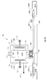
- FIG 3A is an illustration showing the electroplating head 100 being applied in an electroplating process, in accordance with one embodiment of the present invention.
- Each component of the electroplating head 100 is the same as previously described with respect to Figures 1 and 2.
- the electroplating head 100 is moved over the wafer 307 in a direction 401 such that the processing area 201 remains substantially parallel with and proximate to the upper surface of the wafer 307.
- the electroplating head 100 is traversed over the wafer 307, the meniscus 305 is also traversed over the wafer.
- the electroplating head 100 is configured such that the meniscus can be traversed over an entirety of the upper surface of the wafer during the electroplating operation.
- the wafer 307 is held by a wafer support 403.
- Each of a first electrode 405A and a second electrode 405B is located proximate to a periphery of the wafer support 403. Additionally, the second electrode 405B is located at a position that is substantially opposite from the first electrode 405A relative to the wafer support 405.
- the first electrode 405A is disposed at a first position near the periphery of the wafer support 403, such that the first position resides along a first peripheral half of the wafer support 403.
- the second electrode 405B is disposed at a second position near the periphery of the wafer support 403, such that the second position resides along a second peripheral half of the wafer support 403 that is exclusive of the first peripheral half of the wafer support 403.
- Each of the first electrode 405A and the second electrode 405B is configured to be moved to electrically connect to and disconnect from the wafer 307 as indicated by arrows 407A and 407B, respectively.
- the movement of the electrodes 405A and 405B to connect with and disconnect from the wafer 307 can be conducted in an essentially limitless number of ways.
- the electrodes 405A and 405B can be moved linearly in a plane aligned with the wafer.
- the electrodes 405A and 405B having a sufficient elongated shape and being oriented in a coplanar arrangement with the wafer 307 can be moved in a rotational manner to contact the wafer.
- the shape of the electrodes 405A and 405B can be defined in a number of different ways.
- the electrodes 405A and 405B can be substantially rectangular in shape.
- the electrodes 405A and 405B can be rectangular in shape with the exception of a wafer contacting edge which can be defined to follow a curvature of the wafer periphery.
- the electrodes 405A and 405B can be C-shaped. It should be understood, that the present invention requires at least two electrodes that can be independently manipulated to electrically connect with and disconnect from a wafer 307.
- fluid shields 409A arid 409B are provided to protect the first and second electrodes 405A and 405B, respectively, from exposure to the meniscus 305 of electroplating solution as the electroplating head 100 and meniscus 305 traverses thereabove.
- each of the first and second electrodes 405A/405B is controllable to be moved away from the wafer 307 and retracted beneath its respective fluid shield 409A/409B, as the electroplating head 100 and meniscus 305 of electroplating solution traverses thereabove.
- the anodes 115A/115B and at least one of the first and second electrodes 405A/405B are electrically connected to a power supply such that a voltage potential exist therebetween.
- the first electrode 405A is moved to be electrically connected to the wafer 307 such that the negative polarity 309 is established across the upper surface of the wafer 307.
- an electric current will flow through the electroplating solution (defined by the analyte, catalyte, and meniscus) between the anodes 115A/115B and the first electrode 405A.
- the electric current enables the electroplating reactions to occur at portions of the upper surface of the wafer 307 that are exposed to the meniscus 305.
- the portions of the upper surface of the wafer 307 that are exposed to the meniscus 305 serve as the cathode in the electroplating process.
- the first electrode 405A remains connected to the wafer 307 as the electroplating head 100 traverses away from the second electrode 405B toward the first electrode 405A.
- the second electrode 405B is maintained in the retracted position until the electroplating head 100 and meniscus 305 is a sufficient distance away from the second electrode 405B to ensure that the second electrode 405B is not exposed to electroplating solution.
- connection of the first electrode 405A and the second electrode 405B to the wafer 307 is managed to optimize a current distribution present at the portion of the upper surface of the wafer 307 that is in contact with the meniscus 305.
- transition from connection of the first electrode 405A to connection of the second electrode 405B occurs when the processing area 201 of the electroplating head 100 is substantially near a centerline of the upper surface of the wafer 307, wherein the centerline is oriented to be perpendicular to a traversal direction of the electroplating head 100.
- connection of the first electrode 405A to connection of the second electrode 405B is maintained until the second electrode 405B is connected. Once the second electrode 405B is connected to the wafer 307, the first electrode 405A is disconnected from the wafer 307. Maintaining at least one electrode connected to the wafer 307 serves to minimize a potential for gaps or deviations in material deposition produced by the electroplating process.
- Figure 3B is an illustration showing a continuation of the electroplating process depicted in Figure 3A, in accordance with one embodiment of the present invention.
- Figure 3B shows the first and second electrodes 405A/405B following transition from connection of the first electrode 405A to connection of the second electrode 405B.
- Figure 3B shows the electroplating head 100 continuing to traverse over the wafer 307 toward the first electrode 405A.
- the second electrode 405B is shown connected to the wafer 307.
- the first electrode 405A is shown disconnected from the wafer 307 and retracted beneath the fluid shield 409A to be sheltered from the approaching meniscus 305.
- the electric current flows through the electroplating solution (defined by the analyte, catalyte, and meniscus) between the anodes 115A/115B and the second electrode 405B.
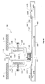
- Figure 4A is an illustration showing the electroplating head 100 being applied in an electroplating process, in accordance with another embodiment of the present invention.
- the arrangement depicted in Figure 4A is equivalent to that of Figure 3A with the exception that the wafer support 403, electrodes 405A/4058, and fluid shields 409A/409B are configured to be moved together in a linear direction 503, below the electroplating head 100 which is maintained in a fixed position secured to support structure 501.
- the processing area 201 of the electroplating head 100 is oriented in a manner similar to that previously discussed with respect to Figure 3A.
- the electrodes 405A/405B are controlled to electrically connect to and disconnect from the wafer 307 based on the processing area 201 and meniscus 305 location, as previously described with respect to Figures 3A and 3B. It should be appreciated that since the apparatus of Figure 4A does not require movement of equipment above the wafer 307, it is conceivable that the apparatus of Figure 4A will allow for easier prevention of unwanted foreign particle deposition on the upper surface of the wafer 307.
- Figure 4B is an illustration showing a continuation of the electroplating process depicted in Figure 4A, in accordance with one embodiment of the present invention.
- Figure 4B shows the first and second electrodes 405A/405B following transition from connection of the first electrode 405A to connection of the second electrode 405B.
- Figure 4B shows the wafer 307 continuing to be traversed beneath the electroplating head 100 such that the meniscus 305 continues to move toward the first electrode 405A.
- the second electrode 405B is shown connected to the wafer 307.
- the first electrode 405A is shown disconnected from the wafer 307 and retracted beneath the fluid shield 409A to be sheltered from the approaching meniscus 305.
- FIG. 5 is an illustration showing an arrangement of wafer surface conditioning devices configured to follow the electroplating head 100 as it traverses over the wafer 307, in accordance with one embodiment of the present invention.
- each wafer surface condition device is represented as a vent configured to apply or remove fluid from the upper surface of the wafer 307.
- Each vent is configured to have an adequately sized flow area to apply and remove fluids at a sufficient rate. It should be appreciated that each depicted vent can be connected to a variety of equipment, e.g., hoses, pumps, metrology, reservoirs, etc., capable of controlling fluid application and removal.
- a first vent 505 provides a vacuum to remove fluids from the surface of the wafer 307 following traversal of the meniscus 305 thereover.
- a second vent 507 applies a rinsing fluid to the surface of the wafer 307.
- the rinsing fluid is deionized water.
- any rinsing fluid suitable for use in wafer processing applications can be used.
- a third vent 509 provides a vacuum to remove fluids from the surface of the wafer 307.
- a fourth vent 511 can be used to apply an isopropyl alcohol (IPA)/nitrogen mixture to the surface of the wafer 307.
- IPA isopropyl alcohol
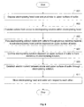
- FIG. 6 is an illustration showing a flowchart of a method for operating an electroplating head, in accordance with one embodiment of the present invention.
- the method includes an operation 601 for disposing the electroplating head over and proximate to an upper surface of a wafer.
- An operation 603 is then provided for transferring cations from an anode to an electroplating solution within the electroplating head.
- the operation 603 is performed by flowing the electroplating solution over a membrane used to confine an analyte, wherein the membrane is capable of transmitting cations from the analyte to the electroplating solution.
- the electroplating solution laden with cations is flowed through a porous resistive material to exit the electroplating head. Upon exiting the electroplating head, the cation laden electroplating solution is disposed on the upper surface of the wafer.
- the method further includes an operation 607 for confining the electroplating solution disposed on the upper surface of the wafer to form a meniscus of electroplating solution.
- the meniscus of electroplating solution is maintained within a region between the porous resistive material and the upper surface of the wafer directly below the porous resistive material.
- electroplating solution is removed from the meniscus in order to establish a flow of electroplating solution through the meniscus.
- an electric current is established between the anode and the upper surface of the wafer through the electroplating solution.
- the porous resistive material causes the electric current to be uniformly distributed across the upper surface of the wafer in contact with the meniscus of electroplating solution.
- the electric current causes the cations within the meniscus of electroplating solution to be attracted to and plated on the upper surface of the wafer.
- the method further includes an operation 611 in which the electroplating head and wafer are controlled to be moved with respect to each other.
- the wafer is maintained in a fixed position and the electroplating head is moved over the wafer such that an entirety of the upper surface of the wafer is exposed to the meniscus of electroplating solution.
- the electroplating head is maintained in a fixed position and the wafer is moved under the electroplating head such that an entirety of the upper surface of the wafer is exposed to the meniscus of electroplating solution.
- conventional electroplating systems require systematic replenishment, or spiking, of the electroplating solution.
- the systematic replenishment of the electroplating solution requires sophisticated real-time chemical assay capability to determine whether the electroplating solution is within process control limits.
- the convention electroplating system requires reclamation of the electroplating solution in order to control process costs.
- the electroplating head and associated meniscus of the present invention provides a confined electroplating reaction region that allows for implementation of a low-volume use-and-discard approach for managing chemistry of the electroplating solution, i.e., the separate analyte and catalyte.
- a low-volume use-and-discard approach for managing chemistry of the electroplating solution, i.e., the separate analyte and catalyte.
- the present invention allows for implementation of a cost effective use-and-discard method for electroplating solution management.
- expensive chemical metrology, spiking, recirculation, and reclamation capabilities are not required to maintain tight process control during the electroplating process performed using the electroplating system of the present invention.
- porous resistive material allows effects due to a resistivity of the upper surface of the wafer, particularly at the wafer edges, to be decoupled and minimized, thereby improving the uniformity of the subsequent plating process.
- the conventional full-wafer electroplating system requires uniformly distributed electrodes about the periphery of the wafer, wherein a resistance for each of the uniformly distributed electrodes is matched.
- the presence of an asymmetric contact resistance from one electrode to another will cause a non-uniform current distribution across the wafer, thus resulting in a non-uniform material deposition across the wafer.
- Use of the porous resistive material, as described with respect to the present invention allows the current flux to be uniformly distributed across the wafer surface area being plated, regardless of the number of electrodes and contact resistance of the electrodes.
Landscapes
- Chemical & Material Sciences (AREA)
- Engineering & Computer Science (AREA)
- Chemical Kinetics & Catalysis (AREA)
- Electrochemistry (AREA)
- Materials Engineering (AREA)
- Metallurgy (AREA)
- Organic Chemistry (AREA)
- Electroplating Methods And Accessories (AREA)
- Electrodes Of Semiconductors (AREA)
Applications Claiming Priority (1)
| Application Number | Priority Date | Filing Date | Title |
|---|---|---|---|
| US10/879,396 US7563348B2 (en) | 2004-06-28 | 2004-06-28 | Electroplating head and method for operating the same |
Publications (2)
| Publication Number | Publication Date |
|---|---|
| EP1612298A2 true EP1612298A2 (de) | 2006-01-04 |
| EP1612298A3 EP1612298A3 (de) | 2011-06-08 |
Family
ID=35056974
Family Applications (1)
| Application Number | Title | Priority Date | Filing Date |
|---|---|---|---|
| EP05253928A Withdrawn EP1612298A3 (de) | 2004-06-28 | 2005-06-24 | Elektroplattierungskopf und Verfahren zu dessen Gebrauch |
Country Status (8)
| Country | Link |
|---|---|
| US (2) | US7563348B2 (de) |
| EP (1) | EP1612298A3 (de) |
| JP (1) | JP4955942B2 (de) |
| KR (1) | KR101167539B1 (de) |
| CN (1) | CN1737207B (de) |
| MY (1) | MY159475A (de) |
| SG (3) | SG185337A1 (de) |
| TW (1) | TWI292001B (de) |
Cited By (2)
| Publication number | Priority date | Publication date | Assignee | Title |
|---|---|---|---|---|
| EP3552746A1 (de) * | 2018-04-10 | 2019-10-16 | Siemens Aktiengesellschaft | Vorrichtung zum selektiven elektrochemischen bearbeiten von werkstücken und anlage zum herstellen eines werkstücks mit einer solchen vorrichtung |
| IT201900007878A1 (it) * | 2019-06-03 | 2020-12-03 | C D T Centro Depurazione Toscano Srl | Impianto galvanostatico per la gestione della distribuzione dello spessore di riporti galvanici ed il procedimento per ottenerli |
Families Citing this family (25)
| Publication number | Priority date | Publication date | Assignee | Title |
|---|---|---|---|---|
| US7592259B2 (en) | 2006-12-18 | 2009-09-22 | Lam Research Corporation | Methods and systems for barrier layer surface passivation |
| WO2006082462A1 (en) * | 2005-02-04 | 2006-08-10 | Edk Research Ag | Device for the electrolytic surface working of metals |
| US7811423B2 (en) * | 2006-10-06 | 2010-10-12 | Lam Research Corporation | Proximity processing using controlled batch volume with an integrated proximity head |
| US20080152823A1 (en) * | 2006-12-20 | 2008-06-26 | Lam Research Corporation | Self-limiting plating method |
| US7794530B2 (en) * | 2006-12-22 | 2010-09-14 | Lam Research Corporation | Electroless deposition of cobalt alloys |
| US7521358B2 (en) * | 2006-12-26 | 2009-04-21 | Lam Research Corporation | Process integration scheme to lower overall dielectric constant in BEoL interconnect structures |
| US8323460B2 (en) * | 2007-06-20 | 2012-12-04 | Lam Research Corporation | Methods and systems for three-dimensional integrated circuit through hole via gapfill and overburden removal |
| JP2011017056A (ja) * | 2009-07-09 | 2011-01-27 | Sumitomo Chemical Co Ltd | 金型の処理方法 |
| US10233556B2 (en) | 2010-07-02 | 2019-03-19 | Lam Research Corporation | Dynamic modulation of cross flow manifold during electroplating |
| US9523155B2 (en) | 2012-12-12 | 2016-12-20 | Novellus Systems, Inc. | Enhancement of electrolyte hydrodynamics for efficient mass transfer during electroplating |
| US9624592B2 (en) | 2010-07-02 | 2017-04-18 | Novellus Systems, Inc. | Cross flow manifold for electroplating apparatus |
| JP5949171B2 (ja) * | 2012-05-31 | 2016-07-06 | 三菱電機株式会社 | 半導体装置の製造方法 |
| KR101481456B1 (ko) * | 2012-12-27 | 2015-01-13 | 한국기계연구원 | 자력형 시료홀더 |
| US9670588B2 (en) | 2013-05-01 | 2017-06-06 | Lam Research Corporation | Anisotropic high resistance ionic current source (AHRICS) |
| CN105895904B (zh) * | 2014-08-13 | 2019-02-22 | 孚能科技(赣州)有限公司 | 制备和回收锂离子电池的正极活性材料的方法 |
| US9816194B2 (en) | 2015-03-19 | 2017-11-14 | Lam Research Corporation | Control of electrolyte flow dynamics for uniform electroplating |
| US10014170B2 (en) | 2015-05-14 | 2018-07-03 | Lam Research Corporation | Apparatus and method for electrodeposition of metals with the use of an ionically resistive ionically permeable element having spatially tailored resistivity |
| US10364505B2 (en) | 2016-05-24 | 2019-07-30 | Lam Research Corporation | Dynamic modulation of cross flow manifold during elecroplating |
| EP3485068B1 (de) | 2016-07-13 | 2026-04-08 | Iontra Inc | Elektrochemische verfahren, vorrichtungen und zusammensetzungen |
| US11214884B2 (en) | 2017-07-11 | 2022-01-04 | University Of South Florida | Electrochemical three-dimensional printing and soldering |
| US11001934B2 (en) | 2017-08-21 | 2021-05-11 | Lam Research Corporation | Methods and apparatus for flow isolation and focusing during electroplating |
| US10781527B2 (en) | 2017-09-18 | 2020-09-22 | Lam Research Corporation | Methods and apparatus for controlling delivery of cross flowing and impinging electrolyte during electroplating |
| IT201800009071A1 (it) * | 2018-10-01 | 2020-04-01 | Rise Tech Srl | Realizzazione di strutture multi-componente tramite menischi dinamici |
| CN114182330B (zh) * | 2021-11-12 | 2023-03-24 | 东莞市点金表面处理有限公司 | 电镀装置 |
| DE102024131083A1 (de) * | 2024-10-24 | 2026-04-30 | Hartchrom Beck GmbH | Galvanikvorrichtung und Verfahren zur Abscheidung einer Galvanikschicht sowie Werkstück mit einer Galvanikschicht |
Family Cites Families (26)
| Publication number | Priority date | Publication date | Assignee | Title |
|---|---|---|---|---|
| BE570709A (de) * | ||||
| US3751343A (en) * | 1971-06-14 | 1973-08-07 | A Macula | Brush electroplating metal at increased rates of deposition |
| US3963588A (en) * | 1975-04-21 | 1976-06-15 | United States Steel Corporation | Coalescent-jet apparatus and method for high current density preferential electroplating |
| GB1602404A (en) * | 1978-04-06 | 1981-11-11 | Ibm | Electroplating of chromium |
| JPH0382787A (ja) * | 1989-08-25 | 1991-04-08 | Omron Corp | 部分メッキ装置 |
| US5660642A (en) | 1995-05-26 | 1997-08-26 | The Regents Of The University Of California | Moving zone Marangoni drying of wet objects using naturally evaporated solvent vapor |
| JPH10130878A (ja) * | 1996-11-01 | 1998-05-19 | Asahi Glass Co Ltd | 電解ニッケルめっき方法 |
| US6398975B1 (en) | 1997-09-24 | 2002-06-04 | Interuniversitair Microelektronica Centrum (Imec) | Method and apparatus for localized liquid treatment of the surface of a substrate |
| KR20010024368A (ko) * | 1997-09-30 | 2001-03-26 | 세미툴 인코포레이티드 | 접촉식 세정 작업을 위한 주 반응 챔버 외측에 보조전극을 구비하는 전기도금 시스템 |
| US6962649B2 (en) * | 1998-07-10 | 2005-11-08 | Semitool, Inc. | Contact assemblies, methods for making contact assemblies, and machines with contact assemblies for electrochemical processing of microelectronic workpieces |
| US6402923B1 (en) * | 2000-03-27 | 2002-06-11 | Novellus Systems Inc | Method and apparatus for uniform electroplating of integrated circuits using a variable field shaping element |
| US6409904B1 (en) * | 1998-12-01 | 2002-06-25 | Nutool, Inc. | Method and apparatus for depositing and controlling the texture of a thin film |
| US6902659B2 (en) | 1998-12-01 | 2005-06-07 | Asm Nutool, Inc. | Method and apparatus for electro-chemical mechanical deposition |
| JP3639134B2 (ja) * | 1998-12-25 | 2005-04-20 | 株式会社荏原製作所 | 基板めっき装置 |
| US7264698B2 (en) * | 1999-04-13 | 2007-09-04 | Semitool, Inc. | Apparatus and methods for electrochemical processing of microelectronic workpieces |
| JP3877911B2 (ja) | 1999-07-08 | 2007-02-07 | 株式会社荏原製作所 | めっき装置 |
| JP2001049498A (ja) | 1999-08-10 | 2001-02-20 | Ebara Corp | めっき装置 |
| US20020121290A1 (en) | 1999-08-25 | 2002-09-05 | Applied Materials, Inc. | Method and apparatus for cleaning/drying hydrophobic wafers |
| US6632335B2 (en) * | 1999-12-24 | 2003-10-14 | Ebara Corporation | Plating apparatus |
| US6547937B1 (en) * | 2000-01-03 | 2003-04-15 | Semitool, Inc. | Microelectronic workpiece processing tool including a processing reactor having a paddle assembly for agitation of a processing fluid proximate to the workpiece |
| US6495005B1 (en) | 2000-05-01 | 2002-12-17 | International Business Machines Corporation | Electroplating apparatus |
| US6478936B1 (en) * | 2000-05-11 | 2002-11-12 | Nutool Inc. | Anode assembly for plating and planarizing a conductive layer |
| JP2002254248A (ja) * | 2001-02-28 | 2002-09-10 | Sony Corp | 電解加工装置 |
| US7128823B2 (en) * | 2002-07-24 | 2006-10-31 | Applied Materials, Inc. | Anolyte for copper plating |
| US7247222B2 (en) * | 2002-07-24 | 2007-07-24 | Applied Materials, Inc. | Electrochemical processing cell |
| US6855239B1 (en) * | 2002-09-27 | 2005-02-15 | Rahul Jairath | Plating method and apparatus using contactless electrode |
-
2004
- 2004-06-28 US US10/879,396 patent/US7563348B2/en not_active Expired - Fee Related
-
2005
- 2005-06-22 MY MYPI20052852A patent/MY159475A/en unknown
- 2005-06-24 EP EP05253928A patent/EP1612298A3/de not_active Withdrawn
- 2005-06-27 JP JP2005186284A patent/JP4955942B2/ja not_active Expired - Fee Related
- 2005-06-28 CN CN2005100896208A patent/CN1737207B/zh not_active Expired - Fee Related
- 2005-06-28 KR KR1020050056630A patent/KR101167539B1/ko not_active Expired - Fee Related
- 2005-06-28 SG SG2012079166A patent/SG185337A1/en unknown
- 2005-06-28 TW TW094121621A patent/TWI292001B/zh not_active IP Right Cessation
- 2005-06-28 SG SG200904329-0A patent/SG153857A1/en unknown
- 2005-06-28 SG SG200504758A patent/SG118432A1/en unknown
-
2009
- 2009-06-10 US US12/482,171 patent/US8419917B2/en not_active Expired - Fee Related
Cited By (3)
| Publication number | Priority date | Publication date | Assignee | Title |
|---|---|---|---|---|
| EP3552746A1 (de) * | 2018-04-10 | 2019-10-16 | Siemens Aktiengesellschaft | Vorrichtung zum selektiven elektrochemischen bearbeiten von werkstücken und anlage zum herstellen eines werkstücks mit einer solchen vorrichtung |
| WO2019197127A1 (de) * | 2018-04-10 | 2019-10-17 | Siemens Aktiengesellschaft | Vorrichtung zum selektiven elektrochemischen bearbeiten von werkstücken und anlage zum herstellen eines werkstücks mit einer solchen vorrichtung |
| IT201900007878A1 (it) * | 2019-06-03 | 2020-12-03 | C D T Centro Depurazione Toscano Srl | Impianto galvanostatico per la gestione della distribuzione dello spessore di riporti galvanici ed il procedimento per ottenerli |
Also Published As
| Publication number | Publication date |
|---|---|
| US7563348B2 (en) | 2009-07-21 |
| SG118432A1 (en) | 2006-01-27 |
| CN1737207A (zh) | 2006-02-22 |
| CN1737207B (zh) | 2010-09-01 |
| MY159475A (en) | 2017-01-13 |
| KR20060048645A (ko) | 2006-05-18 |
| TW200609386A (en) | 2006-03-16 |
| US20090242413A1 (en) | 2009-10-01 |
| EP1612298A3 (de) | 2011-06-08 |
| US8419917B2 (en) | 2013-04-16 |
| US20050284748A1 (en) | 2005-12-29 |
| SG153857A1 (en) | 2009-07-29 |
| SG185337A1 (en) | 2012-11-29 |
| JP2006009154A (ja) | 2006-01-12 |
| KR101167539B1 (ko) | 2012-07-20 |
| TWI292001B (en) | 2008-01-01 |
| JP4955942B2 (ja) | 2012-06-20 |
Similar Documents
| Publication | Publication Date | Title |
|---|---|---|
| US8419917B2 (en) | Electroplating head and method for operating the same | |
| US8048283B2 (en) | Method and apparatus for plating semiconductor wafers | |
| KR102272508B1 (ko) | 이방성 고 저항 이온성 전류 소스 | |
| US6365017B1 (en) | Substrate plating device | |
| US20160273119A1 (en) | Control of electrolyte flow dynamics for uniform electroplating | |
| US7390382B2 (en) | Reactors having multiple electrodes and/or enclosed reciprocating paddles, and associated methods | |
| US7169705B2 (en) | Plating method and plating apparatus | |
| US20100006444A1 (en) | Plating apparatus and plating method for forming magnetic film | |
| US11643744B2 (en) | Apparatus for electrochemically processing semiconductor substrates | |
| CN1957115A (zh) | 用于电镀浴化学剂控制的方法 | |
| US7828951B2 (en) | Wafer support apparatus for electroplating process and method for using the same | |
| KR100465465B1 (ko) | 전해 도금 장치 및 전해 도금 방법 | |
| KR20040007399A (ko) | 반도체 제조를 위한 원격 2차 양극을 갖는 도금 시스템 | |
| CN101288165B (zh) | 在用于液晶显示器的玻璃基板上制造导电特征的方法和装置 | |
| JP2005068494A (ja) | 薄膜処理装置、薄膜処理方法、薄膜トランジスタおよび表示装置 | |
| Matsuda et al. | Electroplating performance enhancement by controlling resistivity of electrolyte with porous materials for advanced Cu metallization | |
| KR20070059351A (ko) | 전기 도금 장치 |
Legal Events
| Date | Code | Title | Description |
|---|---|---|---|
| PUAI | Public reference made under article 153(3) epc to a published international application that has entered the european phase |
Free format text: ORIGINAL CODE: 0009012 |
|
| AK | Designated contracting states |
Kind code of ref document: A2 Designated state(s): AT BE BG CH CY CZ DE DK EE ES FI FR GB GR HU IE IS IT LI LT LU MC NL PL PT RO SE SI SK TR |
|
| AX | Request for extension of the european patent |
Extension state: AL BA HR LV MK YU |
|
| PUAL | Search report despatched |
Free format text: ORIGINAL CODE: 0009013 |
|
| AK | Designated contracting states |
Kind code of ref document: A3 Designated state(s): AT BE BG CH CY CZ DE DK EE ES FI FR GB GR HU IE IS IT LI LT LU MC NL PL PT RO SE SI SK TR |
|
| AX | Request for extension of the european patent |
Extension state: AL BA HR LV MK YU |
|
| RIC1 | Information provided on ipc code assigned before grant |
Ipc: C25D 5/02 20060101ALI20110502BHEP Ipc: C25D 17/14 20060101AFI20051017BHEP |
|
| 17P | Request for examination filed |
Effective date: 20111125 |
|
| AKX | Designation fees paid |
Designated state(s): DE FR |
|
| 17Q | First examination report despatched |
Effective date: 20120907 |
|
| STAA | Information on the status of an ep patent application or granted ep patent |
Free format text: STATUS: THE APPLICATION IS DEEMED TO BE WITHDRAWN |
|
| 18D | Application deemed to be withdrawn |
Effective date: 20140103 |