EP1612681B1 - Identification des emplacements dans un système de bus - Google Patents
Identification des emplacements dans un système de bus Download PDFInfo
- Publication number
- EP1612681B1 EP1612681B1 EP20040015410 EP04015410A EP1612681B1 EP 1612681 B1 EP1612681 B1 EP 1612681B1 EP 20040015410 EP20040015410 EP 20040015410 EP 04015410 A EP04015410 A EP 04015410A EP 1612681 B1 EP1612681 B1 EP 1612681B1
- Authority
- EP
- European Patent Office
- Prior art keywords
- plug
- bus system
- clock edge
- address
- module
- Prior art date
- Legal status (The legal status is an assumption and is not a legal conclusion. Google has not performed a legal analysis and makes no representation as to the accuracy of the status listed.)
- Expired - Lifetime
Links
Images
Classifications
-
- G—PHYSICS
- G06—COMPUTING OR CALCULATING; COUNTING
- G06F—ELECTRIC DIGITAL DATA PROCESSING
- G06F12/00—Accessing, addressing or allocating within memory systems or architectures
- G06F12/02—Addressing or allocation; Relocation
- G06F12/06—Addressing a physical block of locations, e.g. base addressing, module addressing, memory dedication
- G06F12/0646—Configuration or reconfiguration
- G06F12/0669—Configuration or reconfiguration with decentralised address assignment
- G06F12/0676—Configuration or reconfiguration with decentralised address assignment the address being position dependent
Definitions
- the invention relates to a bus system with slots for receiving modules, each slot is assigned an address, and an assembly that is suitable for receiving at one of the slots of such a bus system.
- Such a bus system with slots for receiving modules may be part of a programmable logic controller in an automation system, in particular an industrial automation system.
- a bus system usually has the property that modules can be pulled out without the bus traffic is interrupted to the other modules of the bus system.
- On the backplane run the bus lines to which the modules are connected in parallel.
- this module must be individually addressable. Therefore, usually the individual slots each assigned a unique address in the bus system. An assembly which is connected to a slot with an assigned address can thus be addressed via this address.
- a data packet sent by a subscriber and intended for the respective module thus contains not only the user data but also information about the address of the slot or the module which is recognized by the respective module. However, an assembly on a particular slot must first be told that it has the Subscriber with the respective address is, so that she can react when data is sent on the bus, in which the respective recipient address is entered.
- an address is determined on the basis of a time difference between a first and a second signal, wherein the second signal is delayed on the basis of a delay element on an expansion card and then forwarded to the next slot.
- this arrangement requires an additional switching device at each slot for the subsequent slots.
- the invention has for its object to provide a simplified slot recognition.
- the bus system according to the invention has slots for receiving modules, via a data line of the bus system, a first signal with a first clock edge is transmittable, wherein for assigning each address to a slot the slots a tapped by a recorded on the respective module assembly second Signal can be supplied with a second clock edge, wherein from a time difference between the second and the first clock edge, an address of the respective slot is uniquely determined and wherein each slot by the time difference between the second and the first clock edge by a predefined and thus known in the system time is enlarged.
- the module according to the invention is suitable for receiving at least one of the slots of such a bus system, wherein the module has evaluation means for evaluating the time difference between the second and the first clock edge and for assigning an address in dependence on the result of the evaluation.
- the solution according to the invention makes it possible for the modules to independently recognize the slot or the address of the slot on which they are received.
- the assembly according to the invention advantageously has evaluation means for measuring the time difference between the second and the first clock edge.
- the evaluation means designed as a user-specific integrated circuit (ASIC).
- bus system is used within a programmable logic controller or an automation system, in particular an industrial automation system.
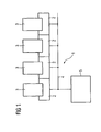
- FIG. 1 shows a bus system 1 with slots 2 for receiving modules 3.
- the slots 2 and thus also recorded in the slots 2 modules 3 are connected to each other via bus lines 4.
- a central processing unit 5 (CPU) is also connected to the bus lines 4.
- the entirety of the bus lines 4 is referred to as a bus.
- the central unit 5 can be accommodated in one of the slots or, as shown, connected to the bus in a different way.
- the central unit 5 communicates with the modules 3 via the bus.
- the modules 3 can communicate with one another via the bus.
- the slots 2 or modules 3 are connected in parallel to the bus lines 4, so that is not affected by a failure or the withdrawal of a module 3, the bus traffic between the remaining modules 3 and the central unit 5 via the bus lines 4.
- Each of the slots 2 is assigned a unique within the bus system 1 address, via which the in the Slots 2 recorded assemblies 3 are each responsive.
- the in the Slots 2 recorded assemblies 3 are each responsive.
- a memory can also be integrated on the module, in which the user can, for example, can write an address using a programmer.
- Another known from the prior art possibility of addressing modules or slots is to lead to each slot an additional line.
- the central unit can select a module with the respective line and inform the module which address it receives. After that, the central unit Send data packets, because the respective module knows its own address and can thus find out for itself which of the sent data packets are intended for them.
- the disadvantage of this solution is that an additional line must be routed to each slot. However, especially in a system with many slots, this means a significantly increased hardware cost.
- the central unit before starting the actual data traffic, the central unit must select each module by means of the additional line and in each case notify it of the address to which it is to react. If an assembly is taken out of such a bus system (eg because it is defective) and replaced by a new module, then the central unit must recognize that the module has been replaced and must in turn transmit the address to the new module.
- the central unit can push data through all modules.
- it first addresses all modules via parallel bus lines to inform them that they should switch to the shift register mode.
- the modules then together form a large shift register with, for example, 128-bit length (eg 16 modules with 8-bit shift registers each).
- the central unit pushes a data packet with exactly 128-bit length over an additional, through-ground line through the modules.
- the module addresses are arranged such that after sliding by 128 bits in each shift register within an assembly exactly the respective module address exists.
- the central unit can inform the modules about the parallel bus lines that they should read the shift register contents and use them as the module address.
- the modules own address is known.
- the central unit can then send data packets to the modules via the parallel bus lines.
- the disadvantage of this solution is in addition to the additional Direction that the modules must have integrated a shift register and must be strung together gapless. As soon as a slot is not occupied, the cross-section shift register is interrupted. The central unit then has no possibility to transmit the modules that are inserted after the gap to the address.
- an address is permanently set at each slot with pins. This requires additional connector pins. For 16 slots, e.g. 4 connector pins required to assign each slot a unique address.
- the bus system according to the invention avoids the disadvantages of the described solutions known from the prior art.
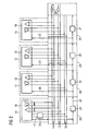
- FIG. 2 shows a bus system in which the slots via a bus line 14, a first signal with a first clock edge and an additional line 40, a second signal is transmitted with a second clock edge.
- the bus system according to FIG. 2 has so-called bus modules 29, which have slots for modules 10-13.
- the received in the first slot assembly 10 is in this case a central unit.
- the remaining three slots contain peripheral modules in this case.
- the connection between the individual slots is made with the bus modules 29.
- the bus is formed by bus lines 14-16.
- the bus lines 14 are designed as so-called write lines, the bus lines 15 as so-called read lines and the bus lines 16 as power supply lines.
- the bus lines 14, 15, also called data lines, are terminated at the physical bus end in each case by a terminating resistor 28.
- the power supply lines 16 are fed via a power supply 17 of the central unit 10.
- the assemblies 10 - 13 each have a user-specific integrated circuit, the so-called Bus ASIC 18, 19, which handles the communication of the modules 10
- the central unit feeds a first electrical signal with a first, instantaneous clock edge.
- the first signal or the first clock edge is therefore instantaneously at all slots.
- the central unit feeds a second electrical signal with a second, with respect to the first clock edge initially undelayed clock edge.
- the clock edge is delayed by time delay means 24 - 27 each for a certain time.
- the time delay means 24 - 27 in the bus module can be realized as active components (eg monoflop) or over propagation times with different line lengths.
- the number of slots that can be addressed in this way has no physical limit. This method can therefore also be used when a large number of modules are to be operated on a bus. If e.g. 100 modules are operated, it is still possible to recognize the slot safely.
- the time difference is then 100 ms in the above example. A very accurate time measurement is very easy to implement in the modules.
- an assembly 11-13 If an assembly 11-13 is plugged into the bus system, it measures the time difference between the clock edge of the respective signal 20-22 and the clock edge of the signal transmitted via the data line, ie the time difference between the occurrence of the signal change on the data line and the occurrence of the Signal change at the delay line. Based on the measured time difference, it recognizes the slot.
- the assignment between the value of the respective time difference and the respective address is known to the module or is carried out automatically by a suitable circuit arrangement for setting the address. The circuit thus allows the assemblies 11-13 to independently recognize their slot.
- the unambiguous assignment of an address to each slot and the unique assignment of the address to a time difference of the module accommodated at the respective slot thus enables an independent address setting.
- the module measures a time difference of 2 ms.
- the invention thus relates to a bus system 1 with slots 2 for receiving modules 3. It is proposed that for simple, automatic assignment of each address to a slot 2 via a data line of the bus system, a first signal with a first clock edge is transmitted and the slots 2 a tapped by a recorded on the respective slot 2 module 3 second signal can be supplied with a second clock edge, wherein from a time difference between the second and the first clock edge, an address of the respective slot 2 is uniquely determined.
- the invention also relates to an assembly 3, which is suitable for receiving at least one of the slots 2 of such a bus system 1, wherein the assembly 3 evaluation means for evaluating the time difference between the second and the first clock edge and for assigning an address depending on the result of Evaluation has.
Landscapes
- Engineering & Computer Science (AREA)
- Theoretical Computer Science (AREA)
- Physics & Mathematics (AREA)
- General Engineering & Computer Science (AREA)
- General Physics & Mathematics (AREA)
- Small-Scale Networks (AREA)
Claims (11)
- Système de bus (1) avec logements (2) pour loger des modules (3), un premier signal pouvant être transmis avec un premier front d'horloge par l'intermédiaire d'une ligne de données du système de bus, un deuxième signal qui peut être prélevé par un module (3) logé dans un logement (2) pouvant être envoyé avec un deuxième front d'horloge aux logements (2) en vue de l'attribution à chaque fois d'une adresse à un logement (2) et une adresse du logement respectif (2) pouvant être déterminée sans équivoque à partir d'une différence temporelle entre le deuxième et le premier front d'horloge,
caractérisé par le fait que la différence temporelle entre le deuxième et le premier front d'horloge est augmentée, par chaque logement, d'un temps prédéfini et donc connu dans le système. - Système de bus selon la revendication 1,
caractérisé par le fait que les logements (2) sont raccordés parallèlement à des lignes de bus (4). - Système de bus selon la revendication 1 ou 2,
caractérisé par le fait que le deuxième signal peut être envoyé aux logements (2) par l'intermédiaire d'une ligne supplémentaire (40). - Système de bus selon l'une des revendications précédentes,
caractérisé par le fait que le deuxième signal peut être envoyé de telle sorte que la différence temporelle entre le deuxième et le premier front d'horloge est différente dans chaque logement (2). - Système de bus selon l'une des revendications précédentes,
caractérisé par le fait que la différence temporelle entre le deuxième et le premier front d'horloge dans chaque logement (2) est augmentée d'un temps prédéfini en comparaison de la différence temporelle entre le deuxième et le premier front d'horloge dans un logement précédent (2). - Système de bus selon l'une des revendications précédentes,
caractérisé par le fait que le deuxième signal est retransmis par un logement précédent à un logement suivant avec un retard égal à un temps prédéfini. - Module (3) qui peut être logé dans au moins l'un des logements (2) d'un système de bus (1) selon l'une des revendications précédentes, le module (3) comportant des moyens d'évaluation pour l'évaluation de la différence temporelle entre le deuxième et le premier front d'horloge et pour l'attribution d'une adresse en fonction du résultat de l'évaluation.
- Module selon la revendication 7,
caractérisé par le fait que les moyens d'évaluation sont prévus pour la mesure de la différence temporelle entre le deuxième et le premier front d'horloge. - Module selon la revendication 7 ou 8,
caractérisé par le fait que les moyens d'évaluation sont réalisés comme un circuit intégré spécifique à l'application. - Commande par programme enregistré avec un système de bus selon l'une des revendications 1 à 6.
- Système automatisé, notamment système automatisé industriel, ayant une commande par programme enregistré selon la revendication 10.
Priority Applications (2)
| Application Number | Priority Date | Filing Date | Title |
|---|---|---|---|
| DE200450007058 DE502004007058D1 (de) | 2004-06-30 | 2004-06-30 | Steckplatzerkennung in einem Bussystem |
| EP20040015410 EP1612681B1 (fr) | 2004-06-30 | 2004-06-30 | Identification des emplacements dans un système de bus |
Applications Claiming Priority (1)
| Application Number | Priority Date | Filing Date | Title |
|---|---|---|---|
| EP20040015410 EP1612681B1 (fr) | 2004-06-30 | 2004-06-30 | Identification des emplacements dans un système de bus |
Publications (2)
| Publication Number | Publication Date |
|---|---|
| EP1612681A1 EP1612681A1 (fr) | 2006-01-04 |
| EP1612681B1 true EP1612681B1 (fr) | 2008-05-07 |
Family
ID=34925558
Family Applications (1)
| Application Number | Title | Priority Date | Filing Date |
|---|---|---|---|
| EP20040015410 Expired - Lifetime EP1612681B1 (fr) | 2004-06-30 | 2004-06-30 | Identification des emplacements dans un système de bus |
Country Status (2)
| Country | Link |
|---|---|
| EP (1) | EP1612681B1 (fr) |
| DE (1) | DE502004007058D1 (fr) |
Family Cites Families (3)
| Publication number | Priority date | Publication date | Assignee | Title |
|---|---|---|---|---|
| DE3303826A1 (de) * | 1983-02-04 | 1984-08-09 | Siemens AG, 1000 Berlin und 8000 München | Speicherprogrammierbare steuerung |
| US5179670A (en) * | 1989-12-01 | 1993-01-12 | Mips Computer Systems, Inc. | Slot determination mechanism using pulse counting |
| AU3437193A (en) * | 1993-01-06 | 1994-08-15 | 3Do Company, The | Expansion bus |
-
2004
- 2004-06-30 DE DE200450007058 patent/DE502004007058D1/de not_active Expired - Lifetime
- 2004-06-30 EP EP20040015410 patent/EP1612681B1/fr not_active Expired - Lifetime
Also Published As
| Publication number | Publication date |
|---|---|
| EP1612681A1 (fr) | 2006-01-04 |
| DE502004007058D1 (de) | 2008-06-19 |
Similar Documents
| Publication | Publication Date | Title |
|---|---|---|
| DE3300260C2 (fr) | ||
| DE3300261C2 (fr) | ||
| EP3131016A1 (fr) | Adressage dynamique | |
| DE3300263A1 (de) | Schaltungsanordnung zur zuteilung des zugriffs zu einer auf anforderungsbasis gemeinsam benutzten sammelleitung | |
| DE20009207U1 (de) | Einrichtung zur Signalübertragung | |
| DE3111555C2 (de) | Verfahren und Vorrichtung zur Informationsspeicherung unter Anwendung früherer Aufzeichnung | |
| DE19532639C2 (de) | Einrichtung zur einkanaligen Übertragung von aus zwei Datenquellen stammenden Daten | |
| DE10128770A1 (de) | Verfahren zum Übertragen von Daten in ein Speicherzellenfeld und Schaltungsanordnung | |
| EP3047635B1 (fr) | Coupleur de bus de terrain pour la connexion de modules à un bus de terrain et procédé d'adressage de ces modules | |
| DE102004046618A1 (de) | Schaltungsanordnung zum Analog/Digital-Wandeln | |
| DE4416879B4 (de) | Steuergerät mit Mitteln zur Umschaltung zwischen zwei Datenleitungen | |
| DE4026581C2 (fr) | ||
| EP1612681B1 (fr) | Identification des emplacements dans un système de bus | |
| EP1612689B1 (fr) | Identification d'emplacements dans un système de bus | |
| DE102019116657B4 (de) | System und Verfahren zur kombinierten Energieübertragung und Datenübertragung in einem Automatisierungssystem | |
| DE4344904A1 (de) | System zur Ankopplung von Aktoren und Sensoren an einen Feldbus | |
| DE19645057C2 (de) | Vorrichtung zur Selektion von Adressenwörtern mittels Demultiplex-Decodierung | |
| DE19645054C2 (de) | Vorrichtung und Verfahren zur Selektion von Adressenwörtern | |
| DE19645055C2 (de) | Elektrische Schaltungsanordnung zur seriellen Auswertung einer bit-Folge | |
| DE102017113538B4 (de) | Steuereinrichtung für einen Leistungshalbleiterschalter | |
| DE3325791C2 (de) | Schaltungsanordnung für mit einer zentralen Steuereinrichtung zusammenarbeitende periphere Einheiten | |
| DE2527236C3 (de) | Anordnung zum Einsetzen von Daten in ein Register | |
| DE19752031C2 (de) | Verfahren und Schaltungsanordnung zur selektiven digitalen Übertragung von Bitfolgen | |
| EP0762246B1 (fr) | Procédé et dispositif de vérification d'une unité de commande | |
| DE10111468B4 (de) | Verfahren und Vorrichtung zur Ermittlung von Eigenschaften gesteckter Module |
Legal Events
| Date | Code | Title | Description |
|---|---|---|---|
| PUAI | Public reference made under article 153(3) epc to a published international application that has entered the european phase |
Free format text: ORIGINAL CODE: 0009012 |
|
| AK | Designated contracting states |
Kind code of ref document: A1 Designated state(s): AT BE BG CH CY CZ DE DK EE ES FI FR GB GR HU IE IT LI LU MC NL PL PT RO SE SI SK TR |
|
| AX | Request for extension of the european patent |
Extension state: AL HR LT LV MK |
|
| 17P | Request for examination filed |
Effective date: 20060206 |
|
| AKX | Designation fees paid |
Designated state(s): DE FR GB IT |
|
| GRAP | Despatch of communication of intention to grant a patent |
Free format text: ORIGINAL CODE: EPIDOSNIGR1 |
|
| GRAS | Grant fee paid |
Free format text: ORIGINAL CODE: EPIDOSNIGR3 |
|
| GRAA | (expected) grant |
Free format text: ORIGINAL CODE: 0009210 |
|
| AK | Designated contracting states |
Kind code of ref document: B1 Designated state(s): DE FR GB IT |
|
| REG | Reference to a national code |
Ref country code: GB Ref legal event code: FG4D Free format text: NOT ENGLISH |
|
| REF | Corresponds to: |
Ref document number: 502004007058 Country of ref document: DE Date of ref document: 20080619 Kind code of ref document: P |
|
| PLBE | No opposition filed within time limit |
Free format text: ORIGINAL CODE: 0009261 |
|
| STAA | Information on the status of an ep patent application or granted ep patent |
Free format text: STATUS: NO OPPOSITION FILED WITHIN TIME LIMIT |
|
| 26N | No opposition filed |
Effective date: 20090210 |
|
| PGFP | Annual fee paid to national office [announced via postgrant information from national office to epo] |
Ref country code: IT Payment date: 20120626 Year of fee payment: 9 |
|
| PG25 | Lapsed in a contracting state [announced via postgrant information from national office to epo] |
Ref country code: IT Free format text: LAPSE BECAUSE OF NON-PAYMENT OF DUE FEES Effective date: 20130630 |
|
| PGFP | Annual fee paid to national office [announced via postgrant information from national office to epo] |
Ref country code: GB Payment date: 20150608 Year of fee payment: 12 |
|
| REG | Reference to a national code |
Ref country code: FR Ref legal event code: PLFP Year of fee payment: 13 |
|
| PGFP | Annual fee paid to national office [announced via postgrant information from national office to epo] |
Ref country code: FR Payment date: 20160615 Year of fee payment: 13 |
|
| PGFP | Annual fee paid to national office [announced via postgrant information from national office to epo] |
Ref country code: DE Payment date: 20160819 Year of fee payment: 13 |
|
| GBPC | Gb: european patent ceased through non-payment of renewal fee |
Effective date: 20160630 |
|
| PG25 | Lapsed in a contracting state [announced via postgrant information from national office to epo] |
Ref country code: GB Free format text: LAPSE BECAUSE OF NON-PAYMENT OF DUE FEES Effective date: 20160630 |
|
| REG | Reference to a national code |
Ref country code: DE Ref legal event code: R119 Ref document number: 502004007058 Country of ref document: DE |
|
| REG | Reference to a national code |
Ref country code: FR Ref legal event code: ST Effective date: 20180228 |
|
| PG25 | Lapsed in a contracting state [announced via postgrant information from national office to epo] |
Ref country code: DE Free format text: LAPSE BECAUSE OF NON-PAYMENT OF DUE FEES Effective date: 20180103 |
|
| PG25 | Lapsed in a contracting state [announced via postgrant information from national office to epo] |
Ref country code: FR Free format text: LAPSE BECAUSE OF NON-PAYMENT OF DUE FEES Effective date: 20170630 |