EP1612689B1 - Identification d'emplacements dans un système de bus - Google Patents
Identification d'emplacements dans un système de bus Download PDFInfo
- Publication number
- EP1612689B1 EP1612689B1 EP04015369A EP04015369A EP1612689B1 EP 1612689 B1 EP1612689 B1 EP 1612689B1 EP 04015369 A EP04015369 A EP 04015369A EP 04015369 A EP04015369 A EP 04015369A EP 1612689 B1 EP1612689 B1 EP 1612689B1
- Authority
- EP
- European Patent Office
- Prior art keywords
- signal
- slot
- address
- bus system
- slots
- Prior art date
- Legal status (The legal status is an assumption and is not a legal conclusion. Google has not performed a legal analysis and makes no representation as to the accuracy of the status listed.)
- Expired - Lifetime
Links
Images



Classifications
-
- G—PHYSICS
- G06—COMPUTING OR CALCULATING; COUNTING
- G06F—ELECTRIC DIGITAL DATA PROCESSING
- G06F12/00—Accessing, addressing or allocating within memory systems or architectures
- G06F12/02—Addressing or allocation; Relocation
- G06F12/06—Addressing a physical block of locations, e.g. base addressing, module addressing, memory dedication
- G06F12/0646—Configuration or reconfiguration
- G06F12/0653—Configuration or reconfiguration with centralised address assignment
- G06F12/0661—Configuration or reconfiguration with centralised address assignment and decentralised selection
-
- G—PHYSICS
- G05—CONTROLLING; REGULATING
- G05B—CONTROL OR REGULATING SYSTEMS IN GENERAL; FUNCTIONAL ELEMENTS OF SUCH SYSTEMS; MONITORING OR TESTING ARRANGEMENTS FOR SUCH SYSTEMS OR ELEMENTS
- G05B19/00—Program-control systems
- G05B19/02—Program-control systems electric
- G05B19/04—Program control other than numerical control, i.e. in sequence controllers or logic controllers
- G05B19/042—Program control other than numerical control, i.e. in sequence controllers or logic controllers using digital processors
-
- H—ELECTRICITY
- H04—ELECTRIC COMMUNICATION TECHNIQUE
- H04L—TRANSMISSION OF DIGITAL INFORMATION, e.g. TELEGRAPHIC COMMUNICATION
- H04L61/00—Network arrangements, protocols or services for addressing or naming
- H04L61/50—Address allocation
- H04L61/5038—Address allocation for local use, e.g. in LAN or USB networks, or in a controller area network [CAN]
-
- G—PHYSICS
- G05—CONTROLLING; REGULATING
- G05B—CONTROL OR REGULATING SYSTEMS IN GENERAL; FUNCTIONAL ELEMENTS OF SUCH SYSTEMS; MONITORING OR TESTING ARRANGEMENTS FOR SUCH SYSTEMS OR ELEMENTS
- G05B2219/00—Program-control systems
- G05B2219/20—Pc systems
- G05B2219/21—Pc I-O input output
- G05B2219/21056—Decoding on module, module can be inserted anywhere, fixed address in bus connector
-
- H—ELECTRICITY
- H04—ELECTRIC COMMUNICATION TECHNIQUE
- H04L—TRANSMISSION OF DIGITAL INFORMATION, e.g. TELEGRAPHIC COMMUNICATION
- H04L2101/00—Indexing scheme associated with group H04L61/00
- H04L2101/60—Types of network addresses
- H04L2101/618—Details of network addresses
- H04L2101/622—Layer-2 addresses, e.g. medium access control [MAC] addresses
Definitions
- the invention relates to a bus system with slots for receiving modules, each slot is assigned an address, and an assembly that is suitable for receiving at one of the slots of such a bus system.
- Such a bus system with slots for receiving modules may be part of a programmable logic controller in an automation system, in particular an industrial automation system.
- a bus system usually has the property that modules can be pulled out without the bus traffic is interrupted to the other modules of the bus system.
- On the backplane run the bus lines to which the modules are connected in parallel.
- CPU Central Processing Unit
- this module must be individually addressable. Therefore, usually the individual slots each assigned a unique address in the bus system. An assembly which is connected to a slot with an assigned address can thus be addressed via this address.
- a data packet sent by a subscriber and intended for the respective module thus contains not only the user data but also information about the address of the slot or the module which is recognized by the respective module. However, an assembly on a particular slot must first be told that it has the Subscriber with the respective address is, so that she can react when data is sent on the bus, in which the respective recipient address is entered.
- the invention has for its object to enable a simple, automatic slot recognition.
- the bus system according to the invention has slots for accommodating modules, it being possible to supply an electrical signal which can be tapped off by an assembly picked up at the respective slot for the assignment of an address to a slot, wherein an address of the respective slot can be determined uniquely.
- the module according to the invention is suitable for receiving at least one of the slots of such a bus system, wherein the module evaluation means for evaluating the value of the physical Has the size of the signal and the assignment of an address depending on the result of the evaluation of the value.
- the solution according to the invention makes it possible for the modules to independently recognize the slot or the address of the slot on which they are received.
- the prior art neither requires a manual address setting, nor do software mechanisms for address transmission in the module have to run in the central unit.
- only a single additional line on the bus is necessary, which is used to supply the signal.
- the slot detection can thus be done automatically and thus particularly fail-safe on the basis of the value of a physical size of the signal.
- the signal can be supplied to the slots in such a way that the value of the physical size of the signal at each slot is different.
- each individual slot can be assigned an address that is unique at least in the bus system, whereby this address results from a predetermined assignment from the respective value of the physical variable to a respective address.
- the signal is a periodic signal and the physical quantity is the frequency of this signal.
- the periodic signal is a rectangular signal.
- the frequency of the signal is particularly easy to evaluate.
- the signal can be supplied in such a way that the frequency of the signal at each slot is a different quotient of a fundamental frequency. Such a frequency division can be realized with relatively little hardware effort.
- the signal is a DC signal and the physical quantity is the voltage of the signal.
- the voltage of a signal can be evaluated in a simple manner and according to a further advantageous embodiment downsize the invention so that the voltage of the signal at each slot is a different quotient of a fundamental voltage.
- the assembly according to the invention advantageously has evaluation means for evaluating the frequency or the voltage of the signal.
- the evaluation means for evaluating the voltage can be designed as an analog converter or as a voltage divider network with downstream comparators.
- the evaluation means are designed as a user-specific integrated circuit (ASIC).
- bus system is used within a programmable logic controller or an automation system, in particular an industrial automation system.
- Figure 1 shows a bus system 1 with slots 2 for receiving modules 3.
- the slots 2 and thus also in the Slots 2 recorded assemblies 3 are connected to each other via bus lines 4.
- a central processing unit 5 (CPU) is also connected to the bus lines 4.
- the entirety of the bus lines 4 is referred to as a bus.
- the central unit 5 can be accommodated in one of the slots or, as shown, connected to the bus in a different way.
- the central unit 5 communicates with the modules 3 via the bus.
- the modules 3 can communicate with one another via the bus.
- the slots 2 or modules 3 are connected in parallel to the bus lines 4, so that is not affected by a failure or the withdrawal of a module 3, the bus traffic between the remaining modules 3 and the central unit 5 via the bus lines 4.
- Each of the slots 2 is assigned a unique within the bus system 1 address, via which the recorded in the slots 2 modules 3 are each responsive.
- the bus system 1 address via which the recorded in the slots 2 modules 3 are each responsive.
- the address setting This makes it error-prone and cumbersome by hand, since the user has to set the address on the new module manually when changing a module, and the new module can not simply be plugged into the bus system or the slot.
- a memory can also be integrated on the module, in which the user can write in an address, for example by means of a programming device.
- Another known from the prior art possibility of addressing modules or slots is to lead to each slot an additional line.
- the central unit can select a module with the respective line and inform the module which address it receives. After that, the central unit can send data packets because the respective module knows its own address and can thus find out for itself which of the data packets sent are intended for it.
- the disadvantage of this solution is that an additional line must be routed to each slot. However, especially in a system with many slots, this means a significantly increased hardware cost.
- the central unit before starting the actual data traffic, the central unit must select each module by means of the additional line and in each case notify it of the address to which it is to react. If an assembly is removed from such a bus system (for example, because it is defective) and replaced with a new module, the central unit must recognize that the module has been changed and must in turn transmit the address to the new module.
- the central unit can push data through all modules.
- it first addresses all modules via parallel bus lines to inform them that they should switch to the shift register mode.
- the Modules then together form a large shift register with, for example, 128-bit length (eg 16 modules with 8-bit shift registers each).
- the central unit pushes a data packet with exactly 128-bit length over an additional, through-ground line through the modules.
- the module addresses are arranged such that after sliding by 128 bits in each shift register within an assembly exactly the respective module address exists.
- the central unit can inform the modules about the parallel bus lines that they should read the shift register contents and use them as the module address.
- the modules own address is known.
- the central unit can then send data packets to the modules via the parallel bus lines.
- a disadvantage of this solution is in addition to the additional line that the modules must have integrated a shift register and must be strung together gapless. As soon as a slot is not occupied, the cross-section shift register is interrupted. The central unit then has no possibility to transmit the modules that are inserted after the gap to the address.
- an address is permanently set at each slot with pins. This requires additional connector pins. For 16 slots, e.g. 4 connector pins required to assign each slot a unique address.
- the bus system according to the invention avoids the disadvantages of the described solutions known from the prior art.
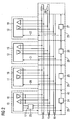
- FIG. 2 shows a bus system in which the signal supplied to the slots is a periodic signal.
- the bus system according to FIG. 2 has so-called bus modules 29, which have slots for modules 10 - 13.
- the received in the first slot assembly 10 is in this case a central unit. In the remaining three slots in this case are peripheral modules.
- the connection between the individual slots is made with the bus modules 29.
- the bus is formed by bus lines 14-16.
- the bus lines 14 are designed as so-called write lines, the bus lines 15 as so-called read lines and the bus lines 16 as power supply lines.
- the bus lines 14, 15 are terminated at the physical bus end in each case by a terminating resistor 28.
- the power supply lines 16 are fed via a power supply 17 of the central unit 10.
- the assemblies 10 - 13 each have a user-specific integrated circuit, the so-called bus ASIC 18, 19, which handles the communication of the modules 10 - 13 via the bus lines 14, 15.
- an additional line 40 is introduced into the bus system.
- the central unit feeds a periodic square wave signal having a known frequency 23 (eg 24 MHz).
- the frequency of the square wave signal is also called the clock frequency.
- the clock frequency is divided down by frequency divider 24 - 27.
- the clock frequency at each slot is divided down to half.
- the assemblies 11 - 13 grab the clock 20 - 22 from the respective slot. Based on the frequency recognize the modules 11 - 13, in which slot they are located. For example, the central unit 10 feeds a signal at the first slot at a frequency of 24 MHz.
- the frequency of the signal is 12,000 kHz, at the next slot 6,000 kHz, etc.
- a module 11-13 If a module 11-13 is plugged into the bus system, it measures the clock frequency 20-22. Based on the clock frequency 20-22 it recognizes the slot.
- the association between the value of the physical quantity of the signal, in this case the frequency of the signal, and the respective address is known to the module or is effected automatically by suitable circuitry for setting the address (see embodiment of FIG 4).
- the circuit thus allows the assemblies 11-13 to independently recognize their slot. Due to the unique assignment of an address to each slot and the unique assignment of the address to a frequency value of the recorded at the respective slot assembly is thus an independent address setting allows.
- the electrical signal which can be picked up by a module 3 accommodated at the respective slot 2 can be any other periodic signal, e.g. B. a sine or triangle signal.
- the signal may also be a pulse train signal.
- a pulse-width-modulated signal could be evaluated in such a way that the pulse width of the pulses can be unambiguously assigned to an address of the respective slot as the physical size of the signal.
- the generation of the slot addresses by frequency division and the slot detection is described in more detail below with reference to the embodiment of Figure 3 on the basis of the voltage level of a signal.
- the same reference numerals as in Figure 2 designate components with the same function.
- an additional line 40 is provided in the bus system, in which case the central unit 10 feeds a signal 33 with a known, fixed voltage (eg with the supply voltage of 5 volts). With voltage dividers 34-38, the voltage at each slot is divided in half.
- the assemblies 11 - 13 pick up a signal 30 - 32 with a respective voltage at the respective slot.
- the assemblies 11 - 13 Based on the voltage of the signal 30 - 32, the assemblies 11 - 13 recognize which slot they are on. If a module is plugged into the bus system, it measures the voltage of the signal which it can pick up at the slot. Based on the voltage, it recognizes the slot.
- the voltage measurement on the assemblies 11-13 can be realized by various methods. This allows a measurement of the analog voltage via analog converter modules. As shown in Figure 3, the voltage can also be determined by means of a voltage divider network of resistors with downstream comparators, eg integrated into a bus ASIC. Such a circuit arrangement thus allows the modules to recognize their own slot.
- the values of the resistors 34-38 according to FIG. 3 are to be selected such that the resistors connected to ground each have twice the resistance value in relation to the series-connected resistors.
- FIG. 4 shows the ASIC internal circuit for the detection of three slots. For the detection of more slots correspondingly more voltage dividers and comparators would have to be introduced.
- a supply voltage of 5 volts is fed in point 48.
- a voltage of 1.25 volts which is the voltage of the DC signal, which picks up the module at its slot.
- the comparator 41 it is achieved that the voltage at the point 40 is detected at a very high impedance and thus is not falsified by the internal circuit.
- the voltage at point 40 comes from the voltage divider on the bus modules.
- the voltage applied at point 48 is the supply voltage of the module.
- the voltage divider comprising the resistor 49 and the resistor 50, which has three times the resistance value compared to the resistor 49, in such a way that a voltage of 3.75 volts is applied at the point 51.
- This divided voltage is fed via the voltage follower 52 to the voltage divider resistors 53, 54, 56, 57, 59, 60, 62.
- the resistors 53, 56, 59 each have half the resistance value in comparison to the resistors 54, 57, 60, 62. Due to this dimensioning of the resistors, the voltage at points 55, 58 and 61 halves in each case.
- the voltages are compared with the comparators 42-44.
- the comparator 42 provides low level (1.25 volts at the P input, 1.88 volts at the N input).
- the comparator 43 provides high level (1.25 volts at the P input, 0.94 volts at the N input).
- the comparator 44 provides high level (1.25 volts at the P input, 0.47 volts at the N input).
- the resistor chain in the ASIC is not designed in the same way as the voltage divider in the bus module.
- the resistor chain in the ASIC an upstream voltage divider from the resistors, 49, 50 connected upstream.
- the voltages at the nodes 55, 58, 61 in the voltage divider network of the ASIC are adjusted to lie exactly between the voltages on the bus modules.
- the invention thus relates to a bus system 1 with slots 2 for receiving modules 3. It is proposed that for simple, automatic assignment of one address to a slot 2 slots 2 a picked up by a recorded on the respective slot 2 module 3 electrical signal can be fed, from the value of a physical size of the signal, an address of the respective slot 2 is uniquely determined.
- the invention also relates to an assembly 3, which is suitable for receiving at least one of the slots 2 of such a bus system 1, wherein the assembly 3 evaluation means for evaluating the value of the physical size of the signal and for assigning an address depending on the result of the evaluation Value has.
Landscapes
- Engineering & Computer Science (AREA)
- Physics & Mathematics (AREA)
- General Physics & Mathematics (AREA)
- Theoretical Computer Science (AREA)
- Computer Networks & Wireless Communication (AREA)
- Signal Processing (AREA)
- Automation & Control Theory (AREA)
- General Engineering & Computer Science (AREA)
- Small-Scale Networks (AREA)
Claims (10)
- Système de bus (1) avec des emplacements (2) pour recevoir des cartes (3), dans lequel, pour associer à chaque fois une adresse à un emplacement (2), un signal électrique pouvant être prélevé par une carte (3) reçue dans l'emplacement respectif (2) peut être envoyé aux emplacements (2) et dans lequel, à partir de la valeur d'une grandeur physique du signal, une adresse de l'emplacement respectif (2) peut être déterminée sans équivoque,
caractérisé par le fait que le signal est un signal périodique et que la grandeur physique est la fréquence du signal, le signal pouvant être envoyé de telle sorte que la fréquence du signal à chaque emplacement (2) est un quotient différent d'une certaine fréquence fondamentale. - Système de bus selon la revendication 1,
caractérisé par le fait que les emplacements (2) sont raccordés en parallèle à des lignes de bus (4). - Système de bus selon la revendication 1 ou 2,
caractérisé par le fait que le signal peut être envoyé aux emplacements (2) par l'intermédiaire d'une ligne supplémentaire (40). - Système de bus selon l'une des revendications précédentes,
caractérisé par le fait que le signal peut être envoyé de telle sorte que la valeur de la grandeur physique du signal est différente à chaque emplacement (2). - Système de bus selon l'une des revendications précédentes,
caractérisé par le fait que le signal périodique est un signal rectangulaire. - Système de bus selon l'une des revendications précédentes,
caractérisé par le fait que la fréquence à chaque emplacement (2) est divisée selon un certain rapport, notamment la moitié, par rapport à la fréquence à un emplacement (2) précédent. - Carte (3), qui peut être reçue dans au moins l'un des emplacements (2) d'un système de bus (1) selon l'une des revendications précédentes, la carte (3) comportant des moyens d'évaluation pour évaluer la valeur de la grandeur physique du signal et pour associer une adresse en fonction du résultat de l'évaluation de la valeur,
caractérisée par le fait que les moyens d'évaluation sont prévus pour l'évaluation de la fréquence du signal. - Carte selon la revendication 7,
caractérisée par le fait que les moyens d'évaluation sont réalisés sous forme de circuit intégré spécifique à l'application. - Commande par programme enregistré avec un système de bus selon l'une des revendications 1 à 6.
- Système d'automatisation, notamment système d'automatisation industriel, avec une commande par programme enregistré selon la revendication 9.
Priority Applications (2)
| Application Number | Priority Date | Filing Date | Title |
|---|---|---|---|
| EP04015369A EP1612689B1 (fr) | 2004-06-30 | 2004-06-30 | Identification d'emplacements dans un système de bus |
| DE502004005783T DE502004005783D1 (de) | 2004-06-30 | 2004-06-30 | Steckplatzerkennung in einem Bussystem |
Applications Claiming Priority (1)
| Application Number | Priority Date | Filing Date | Title |
|---|---|---|---|
| EP04015369A EP1612689B1 (fr) | 2004-06-30 | 2004-06-30 | Identification d'emplacements dans un système de bus |
Publications (2)
| Publication Number | Publication Date |
|---|---|
| EP1612689A1 EP1612689A1 (fr) | 2006-01-04 |
| EP1612689B1 true EP1612689B1 (fr) | 2007-12-26 |
Family
ID=34925556
Family Applications (1)
| Application Number | Title | Priority Date | Filing Date |
|---|---|---|---|
| EP04015369A Expired - Lifetime EP1612689B1 (fr) | 2004-06-30 | 2004-06-30 | Identification d'emplacements dans un système de bus |
Country Status (2)
| Country | Link |
|---|---|
| EP (1) | EP1612689B1 (fr) |
| DE (1) | DE502004005783D1 (fr) |
Cited By (1)
| Publication number | Priority date | Publication date | Assignee | Title |
|---|---|---|---|---|
| CN107342923A (zh) * | 2016-04-28 | 2017-11-10 | 西门子公司 | 具有至少两个总线用户的装置 |
Families Citing this family (3)
| Publication number | Priority date | Publication date | Assignee | Title |
|---|---|---|---|---|
| GB2496886A (en) * | 2011-11-24 | 2013-05-29 | Melexis Technologies Nv | Determining network address of integrated circuit network node |
| CN112838668B (zh) | 2019-11-22 | 2024-05-17 | 华为数字能源技术有限公司 | 一种断路器识别方法、装置和设备 |
| CN116319658A (zh) * | 2023-03-16 | 2023-06-23 | 深圳拓邦股份有限公司 | 多地址识别方法和通信系统 |
Family Cites Families (4)
| Publication number | Priority date | Publication date | Assignee | Title |
|---|---|---|---|---|
| DE19742179C1 (de) * | 1997-09-24 | 1998-11-19 | Siemens Ag | Vorrichtung zur Ankopplung eines Moduls an ein Bus-System und Verfahren zur Adressierung eines an ein Bus-System angekoppelten Moduls mittels einer solchen Vorrichtung |
| US6065068A (en) * | 1998-04-20 | 2000-05-16 | National Instruments Corporation | System for storing and updating configuration information about I/O card and using stored configuration information to configure newly installed I/O card when compatible with old card |
| FR2821453B1 (fr) * | 2001-02-26 | 2005-07-08 | Valeo Climatisation | Procede d'identification des noeuds d'un reseau informatif dans une installation de climatisation de vehicule automobile, et installation de climatisation faisant application du procede |
| WO2003094001A1 (fr) * | 2002-05-02 | 2003-11-13 | Elmos Semiconductor Ag | Procede d'adressage de dispositifs utilisateurs d'un systeme a bus au moyen de courants d'identification |
-
2004
- 2004-06-30 EP EP04015369A patent/EP1612689B1/fr not_active Expired - Lifetime
- 2004-06-30 DE DE502004005783T patent/DE502004005783D1/de not_active Expired - Lifetime
Cited By (3)
| Publication number | Priority date | Publication date | Assignee | Title |
|---|---|---|---|---|
| CN107342923A (zh) * | 2016-04-28 | 2017-11-10 | 西门子公司 | 具有至少两个总线用户的装置 |
| CN107342923B (zh) * | 2016-04-28 | 2020-02-28 | 西门子公司 | 具有至少两个总线用户的装置 |
| US10666456B2 (en) | 2016-04-28 | 2020-05-26 | Siemens Aktiengesellschaft | Arrangement with at least two bus subscribers |
Also Published As
| Publication number | Publication date |
|---|---|
| EP1612689A1 (fr) | 2006-01-04 |
| DE502004005783D1 (de) | 2008-02-07 |
Similar Documents
| Publication | Publication Date | Title |
|---|---|---|
| DE69128521T2 (de) | Nichtflüchtige seriell programmierbare Anordnungen | |
| EP0953848B1 (fr) | Procédé de paramétrage d'un circuit intégré et le circuit intégré correspondant | |
| EP3131016A1 (fr) | Adressage dynamique | |
| EP0624832A2 (fr) | Dispositif de commande électronique pour un poste de soupapes de construction modulaire | |
| EP1450223A1 (fr) | Circuit d'interface universel configurable pour formé l'interface d'entrée/sortie d'un processus | |
| DE20009207U1 (de) | Einrichtung zur Signalübertragung | |
| EP0546455A2 (fr) | Unité de commande électronique pour commuter plusieurs charges électriques | |
| DE3111555C2 (de) | Verfahren und Vorrichtung zur Informationsspeicherung unter Anwendung früherer Aufzeichnung | |
| EP0224707B1 (fr) | Dispositif pour contrôler plusieurs signaux électriques analogues | |
| DE102004046618A1 (de) | Schaltungsanordnung zum Analog/Digital-Wandeln | |
| EP1612689B1 (fr) | Identification d'emplacements dans un système de bus | |
| DE4026581C2 (fr) | ||
| DE102019116657B4 (de) | System und Verfahren zur kombinierten Energieübertragung und Datenübertragung in einem Automatisierungssystem | |
| DE102005043489B4 (de) | Automatisierungstechnische Einrichtung | |
| DE19645057C2 (de) | Vorrichtung zur Selektion von Adressenwörtern mittels Demultiplex-Decodierung | |
| EP4054128B1 (fr) | Procédé d'initialisation d'un système de bus de communication série | |
| EP1612681B1 (fr) | Identification des emplacements dans un système de bus | |
| DE19860465A1 (de) | Verfahren und Vorrichtung zur Kodierung der Adressen von baugleichen Funktionseinheiten | |
| DE19645055C2 (de) | Elektrische Schaltungsanordnung zur seriellen Auswertung einer bit-Folge | |
| DE202016100397U1 (de) | Reihenanordnung | |
| DE102005043488A1 (de) | Automatisierungstechnische Einrichtung | |
| DE102017113538B4 (de) | Steuereinrichtung für einen Leistungshalbleiterschalter | |
| EP4038843B1 (fr) | Système de bus et procédé d'exploitation d'un système de bus | |
| DE3432837A1 (de) | Datenkompressions- und datenexpandiereinrichtung zum uebertragen bzw. speichern von daten | |
| DE1925915A1 (de) | Umsetzer |
Legal Events
| Date | Code | Title | Description |
|---|---|---|---|
| PUAI | Public reference made under article 153(3) epc to a published international application that has entered the european phase |
Free format text: ORIGINAL CODE: 0009012 |
|
| AK | Designated contracting states |
Kind code of ref document: A1 Designated state(s): AT BE BG CH CY CZ DE DK EE ES FI FR GB GR HU IE IT LI LU MC NL PL PT RO SE SI SK TR |
|
| AX | Request for extension of the european patent |
Extension state: AL HR LT LV MK |
|
| 17P | Request for examination filed |
Effective date: 20060206 |
|
| AKX | Designation fees paid |
Designated state(s): DE FR GB IT |
|
| 17Q | First examination report despatched |
Effective date: 20060823 |
|
| GRAP | Despatch of communication of intention to grant a patent |
Free format text: ORIGINAL CODE: EPIDOSNIGR1 |
|
| GRAS | Grant fee paid |
Free format text: ORIGINAL CODE: EPIDOSNIGR3 |
|
| GRAA | (expected) grant |
Free format text: ORIGINAL CODE: 0009210 |
|
| AK | Designated contracting states |
Kind code of ref document: B1 Designated state(s): DE FR GB IT |
|
| REG | Reference to a national code |
Ref country code: GB Ref legal event code: FG4D Free format text: NOT ENGLISH |
|
| GBT | Gb: translation of ep patent filed (gb section 77(6)(a)/1977) |
Effective date: 20080110 |
|
| REF | Corresponds to: |
Ref document number: 502004005783 Country of ref document: DE Date of ref document: 20080207 Kind code of ref document: P |
|
| ET | Fr: translation filed | ||
| PLBE | No opposition filed within time limit |
Free format text: ORIGINAL CODE: 0009261 |
|
| STAA | Information on the status of an ep patent application or granted ep patent |
Free format text: STATUS: NO OPPOSITION FILED WITHIN TIME LIMIT |
|
| 26N | No opposition filed |
Effective date: 20080929 |
|
| PGFP | Annual fee paid to national office [announced via postgrant information from national office to epo] |
Ref country code: IT Payment date: 20120626 Year of fee payment: 9 |
|
| PG25 | Lapsed in a contracting state [announced via postgrant information from national office to epo] |
Ref country code: IT Free format text: LAPSE BECAUSE OF NON-PAYMENT OF DUE FEES Effective date: 20130630 |
|
| PGFP | Annual fee paid to national office [announced via postgrant information from national office to epo] |
Ref country code: GB Payment date: 20150608 Year of fee payment: 12 |
|
| REG | Reference to a national code |
Ref country code: FR Ref legal event code: PLFP Year of fee payment: 13 |
|
| PGFP | Annual fee paid to national office [announced via postgrant information from national office to epo] |
Ref country code: FR Payment date: 20160615 Year of fee payment: 13 |
|
| PGFP | Annual fee paid to national office [announced via postgrant information from national office to epo] |
Ref country code: DE Payment date: 20160819 Year of fee payment: 13 |
|
| GBPC | Gb: european patent ceased through non-payment of renewal fee |
Effective date: 20160630 |
|
| PG25 | Lapsed in a contracting state [announced via postgrant information from national office to epo] |
Ref country code: GB Free format text: LAPSE BECAUSE OF NON-PAYMENT OF DUE FEES Effective date: 20160630 |
|
| REG | Reference to a national code |
Ref country code: DE Ref legal event code: R119 Ref document number: 502004005783 Country of ref document: DE |
|
| REG | Reference to a national code |
Ref country code: FR Ref legal event code: ST Effective date: 20180228 |
|
| PG25 | Lapsed in a contracting state [announced via postgrant information from national office to epo] |
Ref country code: DE Free format text: LAPSE BECAUSE OF NON-PAYMENT OF DUE FEES Effective date: 20180103 |
|
| PG25 | Lapsed in a contracting state [announced via postgrant information from national office to epo] |
Ref country code: FR Free format text: LAPSE BECAUSE OF NON-PAYMENT OF DUE FEES Effective date: 20170630 |